SlideShare una empresa de Scribd logo
1 de 10
Descargar para leer sin conexión
111111 1111111111111111111111111111111111111111111111111111111111111
(12) United States Patent
Bream et al.
(54) HEATSINK WITH HIGH THERMAL
CONDUCTIVITY DIELECTRIC
(75) Inventors: Jeffrey L. Bream, Bethlehem, PA (US);
Stephen A. Ferranti, Rowlett, TX
(US); Madhu Ganesa-Pillai, Dallas,
TX (US); Leon Klafter, Allen, TX
(US); Alan M. Lyons, New Providence,
NJ (US); John Paul Mello, Dallas;
Steven J. Vargo, Midlothian, both of
TX (US)
(73) Assignee: Lucent Technologies Inc., Murray Hill,
NJ (US)
( *) Notice: Subject to any disclaimer, the term of this
patent is extended or adjusted under 35
U.S.C. 154(b) by 0 days.
(21) Appl. No.: 09/252,741
(22)
(51)
(52)
(58)
(56)
Filed: Feb. 19, 1999
Int. Cl? .............................. HOSK l/18; H05K 1!09;
H05K 3/30
U.S. Cl. ......................... 174/260; 174/16.3; 174/252;
361/705; 361/707; 361/708; 165/80.2; 165/185;
165/80.3; 257/707; 257/713; 257/717
Field of Search .................................... 174/260, 16.3,
174/252; 361/708, 707, 704, 705, 719,
720; 165/80.2, 80.3, 185; 257/707, 713,
717
References Cited
U.S. PATENT DOCUMENTS
5,146,981 * 9/1992 Samarov .............................. 165/185
r--- - - - -
r--... 2l:2!:2':
,..-241
240 r-- '242
~
'243
US006225571Bl
(10) Patent No.:
(45) Date of Patent:
US 6,225,571 Bl
May 1, 2001
5,344,795 * 9/1994 Hashemi et a!. ................ 264/272.15
5,533,256 * 7/1996 Call eta!. .............................. 29/840
5,616,888 * 4/1997 McLaughlin et a!. ............... 174/260
5,757,073 * 5/1998 Hoffmeyer ........................... 257/700
5,931,222 * 8/1999 Toy et a!. ............................ 165/80.3
6,011,299 * 1!2000 Brench ................................. 257/660
6,021,044 * 2/2000 Neville, Jr. et a!. ................. 361!700
6,084,775 * 7/2000 Bartley et a!. ....................... 361!705
6,085,833 * 7/2000 Kimura et a!. ....................... 165/185
6,088,226 * 7/2000 Rearick ................................ 361!704
6,154,369 * 11/2000 Martinez, Jr. et a!. .............. 361/719
* cited by examiner
Primary Examiner-Jeffrey Gaffin
Assistant Examiner---Ishwar B. Patel
(57) ABSTRACT
The present invention provides a heatsink for use with a
heat-generating electrical component. The heatsink com-
prises a spine having opposing sides, cooling fins extending
from the spine, and a dielectric layer adhered to at least one
of the opposing sides. The dielectric layer has a thermal
conductivity of at least about 1 W/m0
C. The heatsink may
further comprise a metal layer adhered to the dielectric layer.
The metal layer provides a surface to which an electric
component can be adhered. The heatsink can further include
a heat-generating component adhered to the metal layer. In
another aspect, the heat-generating component is a surface-
mount electrical component adhered to the metal layer with
solder.
;2!:!2
XXl!
16 Claims, 3 Drawing Sheets
- - - r - - - -
~140
r
255 rr,~251
250 '~- r1
~ a!:~r--252
1'-253...._ 'l'
1/
130 .. 110
"100
Prior Mello Patents Master Index
Patent Inventors
6225571 Jeffrey L. Bream,Stephen A. Ferranti,Madhu Ganesa-Pillai, Leon Klafter, Alan M. Lyons, John Paul Mello, Steven J. Vargo
6204452 Armando Rodriguez Valadez, JuanDe Dios Concha Malo, BelisarioSanchez Vazquez, Mario Sanchez Mello
6186799 Keith F. Mello
6186059 Frank C. Mello, Jeffrey A. Williams, Kenneth M. Ware
6125682 Michael Rzasa, Keith Mello
5997368 Keith F. Mello, H.Thomas Nelson, GerhardP. Schwebler
5966982 Keith Mello, H.Thomas Nelson
5957733 Keith F. Mello, Raymond G. Lavoie, ChristopherG. Chadbourne, William J. Lasko, Roger H.Hanks
5956604 Sabrina L. Lee,KevinE. Mello, Steven R. Soss, Toh-Ming Lu, ShyamP. Murarka
5942712 Craig S. Mello
5932456 Arlen Van Draanen, StevenMello
5916424 Charles J. Libby, Donald E. Yansen,Gregory J.Athas, Raymond Hill, RussellMello
5910878 Alfred A. Mello, DonaldL. Pearl
5888104 Keith F. Mello, H.Thomas Nelson
5866427 Jack H. Mendelson, Nancy K. Mello, Tak-Ming Chiu
5820904 Frank C. Mello, Roger S. Williams, Jeffrey A. Williams
5778793 Kathryn M. Mello,Matthew M. Semiao
5775313 Douglas T. Bresette, JohnMello,III
5770249 Frank C. Mello, Jeffrey A. Williams, Roger S. Williams
5759072 Richard Chadbourne,KeithMello,GennaroL. Pecora
5681745 PrzemyslawSzafranski, CharleneM. Mello,Takeshi Sano, Kenneth A. Marx, Charles R. Cantor, David L. Kaplan, Cassandra L. Smith
5679533 PrzemyslawSzafranski, CharleneM. Mello,Takeshi Sano, Kenneth A. Marx, Charles R. Cantor, David L. Kaplan, Cassandra L. Smith
5677154 Arlen Van Draanen, StevenMello
5597606 Lee Kramer, Roger S. Williams,Jeffrey A. Williams, Frank C. Mello, DaleV. Miller
5580597 Lee Kramer, Roger S. Williams,Frank C. Mello, Jeffrey A. Williams, DaleV. Miller
5552406 Jack H. Mendelson, Nancy K. Mello
5542234 Ihor Wyslotsky, Frank C. Mello
5355990 John T. Pitts, Ary O. Mello,Gerald E. Johnson
5287265 Richard A. Hall, Gary J. Mello
5284237 Ary O. Mello, GeraldE. Johnson,Mukunda Pramanik
5226522 Gerald E. Johnson, Mukunda B. Pramanik, Ary O. Mello
5199302 Frank P. Mello
5178559 Craig S. Mello
5156252 Ary O. Mello, GeraldE. Johnson,Arthur McClement
5106670 Ihor Wyslotsky, Frank C. Mello
5092215 William Mello, John Hendrickson
5083700 Frank C. Mello, Jan Gullett
5075341 Jack H. Mendelson, Nancy K. Mello
5054266 Frank C. Mello, Ihor Wyslotsky
4955983 DanielC. Meess,BobbyJ. Jones, Raymond M. Mello, Thomas G. Weiss, Jr., James B. Wright
4934767 Hazen L. Hoyt,III,JonC. Goldman, WilliamR. Mello
4830261 Mark D. Mello, StevenC. Iemma,Ray M. Hill, Charles W. Miller, Jr.,Louis G. Blais, Carl E. Andersen,J. TerenceFeeley
4825088 Balakrishnan R. Nair, RaymondV. Richardson, RaymondM. Mello
4728246 William R. Mello
4722659 Hazen L. Hoyt III, JohnD. Sanders, Jon C.Goldman, WilliamR. Mello
4504824 William R. Mello
4250591 Frank A. Mello
4236654 Frank A. Mello
4098448 Albert M. Sciaky, WilliamR. Mello
4046169 Louis P. Pollono, RaymondM. Mello
3968882 Fabio Mello
U.S. Patent
r-- r--
-....... :x:l!::X
240 ---.
nX
May 1, 2001
100
" 111
140
145
150
170
r-- -
~,---241
r--- 242
1'-.243
Sheet 1 of 3
FIG. 1
120
FIG. 2
r-- -
110
112
130
-
US 6,225,571 Bl
r-- - - r--
--
~ 255 rril~,---251
250-- ,f-~ r.,~ ~f~'--252txxx
140 __ ,. ~'-253
/ ..130 110
"-too
U.S. Patent May 1, 2001
FIG. 3A
240
"""
Sheet 2 of 3
r38
: 343I I
:..--
1
I
I
: 243
I
I
I
I I
US 6,225,571 Bl
241
242
r- - .....
~--~-~--~-~- I ~ '•342
I
__________ j
~38
FIG. 3B 13o
,________,y
140
350
243
242
150
U.S. Patent May 1, 2001 Sheet 3 of 3 US 6,225,571 Bl
FIG. 4
400
(START
410 450
'- _./
HEATSINK ETCH METAL
SPINE SELECTION LAYER
420 460
'- _./
PLACE SCREEN PRINT
DIELECTRIC LAYER SOLDER
430 470
'- PLACE ELECTRONIC_./PLACE
METAL LAYER DEVICES
440 480
'- vHEAT AND REFLOW
PRESSURE CYCLE SOLDER
490
END
US 6,225,571 Bl
1
HEATSINK WITH HIGH THERMAL
CONDUCTIVITY DIELECTRIC
TECHNICAL FIELD OF THE INVENTION
2
Accordingly, what is needed in the art is a heatsink with
a low thermal impedance between the electronic component
and the body of the heatsink while maintaining good dielec-
tric characteristics and eliminating mechanical fasteners.
The present invention is directed, in general, to a heatsink 5
and, more specifically, to a heatsink having an insulating
dielectric with a high thermal conductivity.
SUMMARY OF THE INVENTION
To address the above-discussed deficiencies of the prior
art, the present invention provides a heatsink for use with a
heat-generating electrical component. The heatsink com-BACKGROUND OF THE INVENTION
Because of the ever increasing demand placed on elec-
trical components, in general, electronic designers need to
be able to pack higher powered components closer together
in ever smaller spaces. More power in less space translates
to higher watt densities, and therefore, increased heat gen-
eration. As temperatures rise, the reliability and functionality
of electronic components are impaired dramatically. Expe-
rience has shown that more than 50 percent of electronic
failures are the result of thermal problems. Traditionally,
heatsinks are used to move heat from components generat-
ing the heat to an area where the heat can be dissipated to the
atmosphere or adequate ventilation can be provided to the
heatsink.
Conventional heatsinks use some type of mechanical
method to attach the heat-generating component to the
heatsink. The most common methods are: adhesives, spring
clamping devices, or hold-down brackets with a mechanical
fastener such as a machine screw. These methods generally
require an assembler to make the mechanical attachment of
the component to the heatsink.
Heat-generating electronic devices need to be electrically
isolated from the heatsink in many cases. Currently the
devices are electrically isolated by a thermal interface pad,
which results in a substantial thermal contact resistance.
Typically, in a stamped heatsink assembly, the presence of
the thermal interface pad can contribute up to 50 percent of
the overall thermal resistance, even in the best designs.
However, heat generating devices may be directly mounted
10 prises a spine having opposing sides, cooling fins extending
from the spine, and a dielectric layer adhered to at least one
of the opposing sides. The dielectric layer has a thermal
conductivity of at least about 1 W/m0
C. In one embodiment,
the heatsink further comprises a metal layer adhered to the
15
exposed surface of the dielectric layer. The metal layer is
preferably adhered to exposed surface of the dielectric layer
without the use of conventional adhesives that are typically
used to adhere electrical components to heatsinks. Thus, the
problems associated with the use of such conventional
20
adhesives are avoided. Once attached to the dielectric layer,
the metal layer provides a surface to which an electric
component can be attached. In another aspect of this
embodiment, the heatsink further includes a heat-generating
component adhered or attached to the metal layer. In a
25
particularly advantageous embodiment, the heat-generating
component is a surface-mount electrical component that is
adhered to the metal layer with solder.
In another embodiment, the metal layer is patterned to
form concentric patterns on the dielectric layer to provide a
30
mounting location for electrical components having mount-
ing footprints of different sizes. These concentric patterns
can be used as a self-aligning mark for easily placing or
positioning the electrical components on the metal layer. In
one aspect of this embodiment, the metal layer forms at least
35
three concentric patterns to accommodate any of three
different sizes of electrical components. In a particularly
advantageous embodiment, the concentric patterns provide a
self-aligning pattern for adhering a surface-mountable elec-
trical component thereon during a soldering process.
on the heatsink. In at least one conventional approach, the
entire heatsink is covered with a dielectric material prior to
mounting the device on an intervening metal foil layer. By 40
covering unnecessary areas of the heatsink with the
dielectric, the thermal efficiency of forced convection cool-
ing is significantly reduced. When the device is surface
mounted, the contact resistance is very low, because of the
metal to metal bond between the tab of the device and the
metal foil substrate.
In another embodiment, the electrical component has
electrical leads extending therefrom with each of the elec-
trical leads configured to be received in a corresponding
contact opening within a printed wiring board. The self-
aligning pattern aligns each of the electrical leads with one
45 of the corresponding contact openings, respectively.
In yet another embodiment, the heatsink further includes
a heat-generating component adhered to the dielectric layer.
The dielectric layer, in particularly advantageous
embodiments, comprises material with a thermal conductiv-
There are additional thermal transfer inefficiencies asso-
ciated with the way in which components are conventionally
attached to the heatsink. Although the component surface
and the mating surface appear to be smooth, under adequate
magnification it can be shown that they are actually rough.
When a heatsink is mated with a heat-generating device by
a mechanical means such as a spring clamp or hold-down
bracket, microscopic peaks in the surface of the component
ride upon corresponding microscopic peaks of the heatsink.
Therefore, the two surfaces are not in the close physical
proximity that fosters good heat transference by conduction.
Of course, this poor thermal conductivity results in higher
device temperatures which, in turn, lead to device failures.
Alternatively, adhesives are often used to adhere the elec-
trical component to the heatsink; however, these conven-
tional adhesives also bring disadvantages. For example,
while these adhesives often have good dielectric
characteristics, they are not good thermal conductors, or, if
they are good thermal conductors, they tend to have poor
dielectric characteristics. Thus, these present day adhesives
do have undesirable characteristics.
50 ity ranging from about 2 W/m0
C. to about 15 W/m0
C.
The dielectric layers may be adhered to each of the
opposing sides with a metal layer being adhered to each of
the dielectric layers. In one aspect of this particular
embodiment, the heatsink has an electrical component
55 adhered to each of the metal layers.
The foregoing has outlined, rather broadly, preferred and
alternative features of the present invention so that those
skilled in the art may better understand the detailed descrip-
tion of the invention that follows. Additional features of the
60 invention will be described hereinafter that form the subject
of the claims of the invention. Those skilled in the art should
appreciate that they can readily use the disclosed conception
and specific embodiment as a basis for designing or modi-
fying other structures for carrying out the same purposes of
65 the present invention. Those skilled in the art should also
realize that such equivalent constructions do not depart from
the spirit and scope of the invention in its broadest form.
US 6,225,571 Bl
3
BRIEF DESCRIPTION OF THE DRAWINGS
For a more complete understanding of the present
invention, reference is now made to the following descrip-
tions taken in conjunction with the accompanying drawings,
in which:
FIG. 1 illustrates an end elevational view of one embodi-
ment of a heatsink constructed according to the principles of
the present invention;
FIG. 2 illustrates a side view of the heatsink of FIG. 1;
FIG. 3A illustrates a plan view of three standard sizes of
components affixed to the concentric patterns of the heatsink
of FIG. 1;
FIG. 3B illustrates a partial sectional view of a heat-
generating device and heatsink of FIG. 3A along line
3B-3B; and
FIG. 4 illustrates a flow diagram showing the various
operations conducted during manufacture and assembly of
the heatsink and components illustrated in FIGS. 1 and 2.
DETAILED DESCRIPTION
Referring initially to FIG. 1, illustrated is an end eleva-
tiona! view of one embodiment of a heatsink constructed
according to the principles of the present invention. A
heatsink, generally designated 100, comprises a spine 110,
cooling fins 120, a dielectric layer 130, and a metal layer
140. Also shown are heat-generating devices 150, 160, with
contact leads 152, 162, through contact openings 171 in a
printed wiring board (PWB) 170.
The spine 110 may be constructed of any suitable
material, most commonly aluminum, copper, steel or other
excellent thermal conducting materials. In an alternative
embodiment, the spine 110 may be of aluminum and com-
prise surfaces 111, 112 that have been treated to improve
adhesion between the spine 110 and the dielectric layer 130.
This surface treatment may be accomplished by chemical
cleaning, grit blasting, etching, or anodizing. Adhesion is an
important issue in this application due to the CTE
(coefficient of thermal expansion) mismatch between the
aluminum spine 110 (24 ppm) and the copper-based metal
layer 140 (17 ppm). One who is skilled in the art will
recognize that because of the different CTEs, differing peel
stresses will occur during thermal cycling at the aluminum
spine 110 and dielectric layer 130 junction than at the metal
layer 140 and the dielectric layer 130 junction. The dura-
bility of the adhesive bond strength increases as the selected
surface treatment process moves from cleaning to grit blast-
ing to etching to anodization. For an ac-dc rectifier appli-
cation where the module typically runs warm and in an
indoor environment, grit blasting the aluminum should be
sufficient to achieve good reliability. However, grit blasting
the surface, although an inexpensive process, leaves the
aluminum fins untreated and subject to oxidation and cor-
rosion. A high purity aluminum alloy, which is preferably
>99% pure aluminum, is inherently corrosion resistant.
Other less pure alloys would necessitate a surface treatment
to inhibit corrosion. Any anodization process will both
improve adhesion and prevent corrosion.
Another group of aluminum surface treatments com-
monly used to prevent corrosion are called conversion
coatings. Among commercially available conversion coat-
ings are IrriditeTM and AlodineTM. Most are chromate-based
coatings; however, to avoid the use of carcinogenic chro-
mium solutions, non-chromate based conversions coatings,
such as Alodine 2000, Alodine 300+Deoxylyte® and Ala-
dine™ 5200, are now available and may be used in place of
4
the chromate-based conversion coatings. All of these coat-
ings have been shown to protect aluminum surfaces from
corroswn.
Therefore, in a specific embodiment, the spine 110 may be
5 anodized aluminum. Anodizing is a low-cost metal treat-
ment that improves chemical resistance of the aluminum to
acidic solutions, improves bond strength of the dielectric
layer 130, and provides an added layer of dielectric isolation
between the devices 150, 160 and the spine 110. The cooling
10 fins 120 may be of any design that presents the desired
surface area for heat dissipation. In the illustrated
embodiment, the dielectric layer 130 and metal layer 140
have been applied to the surface of opposing sides 111, 112
of the spine 110. One who is skilled in the art will recognize
15 that the heatsink may also be constructed with a dielectric
layer 130 and metal layer 140 on only one side. The
dielectric layer 130 preferably has a thermal conductivity of
at least about 1 W/m0
C. In an alternative embodiment,
however, the dielectric layer 130 may have a thermal con-
20 ductivity ranging from about 2 W/m0
C. to about 15 W/m0
C. For example, one dielectric material presently available is
T-preg™, which has a thermal conductivity of about 8 W/m0
C. It is also highly desirable that the dielectric layer 130 have
good dielectric characteristics as well. For example, it is
25 desirable that the dielectric layer 130 have a dielectric
strength of about 2500 V. The heat-generating devices 150,
160 may be surface mounted to an exposed surface 140a of
the metal layer 140 by a solder layer 145. When molten,
solder fills the microscopic voids between the irregular
30 surfaces of the metal layer 140 and the heat-generating
device 150, thereby improving surface-to-surface thermal
transmission. In this particular embodiment, the use of
solder in place of the conventional adhesion systems dis-
cussed above substantially improves the thermal conduc-
35 tance between the metal layer 140 and the heat-generating
device 150 due to the molten solder's ability to fill the
microscopic voids.
Referring now to FIG. 2, illustrated is a side view of the
heatsink of FIG. 1. Shown in this view of the heatsink 100
40 are alternative forms of concentric patterns 240, 250, formed
from the metal layer 140 that is adhered to the spine 110. To
form concentric pattern 240, the metal layer 140 may be
formed as a continuous layer on the dielectric layer 130. Of
course, the number of sites 240, 250 are dependent upon the
45 number and sizes of components. The metal layer 140 may
then be photolithographically etched using conventional
methods to form pattern 240 with dielectric areas 232, 233
exposed between adjacent concentric metallic patterns 241,
242, 243. Photolithography enables the formation of all
50 types of circuit designs, including those with small, isolated
traces. Photolithography also enables some circuitry to be
moved from the PWB to the heatsink, saving useful area on
the PWB. However, in the photolithography process, as one
who is skilled in the art will understand, acid is used to etch
55 away unprotected copper areas of the metal layer 140. In this
process, exposed aluminum of the heatsink is subjected to an
acidic environment that will rapidly erode it. Thus, the key
to effectively implementing photolithography is to protect
exposed aluminum surfaces prior to copper layer 140 lami-
60 nation. This can be achieved by anodizing the aluminum as
described above, and sealing the surface with a combination
of nickel acetate and chromic acid. Alternatively, the alu-
minum may be sealed with steam, triethanolamine, sodium
silicate, etc. A discussion of sealing may be found in The
65 Surface Treatment and Finishing of Aluminum and Its
Alloys, 5th Ed., Vol. 2, Chapter 11, "Sealing Anodic Oxide
Coatings," pg. 773-856, incorporated herein by reference.
US 6,225,571 Bl
5
However, it may be desirable to form the metal layer 140
separately as concentric pattern 250 comprising patterns
251, 252, 253 and then affix them to the dielectric layer 130.
Concentric patterns 240 and 250 differ by the absence or
presence of interconnects 255. The interconnects 255 main- 5
tain precise spacing between patterns 251, 252, and 253
during the application of concentric pattern 250 to the
dielectric layer 130. This approach is commonly achieved by
stamping the patterns 250 from a sheet with a lead frame
(not shown). One who is skilled in the art is familiar with 10
lead frame technology. As described above, concentric pat-
tern 240 is formed by etching away the metal layer 140 from
areas 232, 233, the interconnects 255 are not required. Of
course, the number of concentric patterns 240, 250 that may
be formed on the heatsink is dependent upon the size and 15
number of components and the size of the heatsink. For
example, a three inch long heatsink may have up to three
mounting sites on one side for components with TO 218, TO
220 and TO 247 package sizes.
Referring now to FIG. 3A with continuing reference to 20
FIG. 1, illustrated is a plan view of three standard sizes of
components affixed to the concentric patterns of the heatsink
of FIG. 1. In the illustrated embodiment, the essentially-
rectilinear, concentric patterns 240, 250 are sized to accept
surface mounting of three standard sizes 341, 342, 343 25
(dashed lines) of electrical components. Each size fits pre-
cisely to a surface mounting area offered by one of the
patterns 241, 242, 243, respectively. Of course, the number
of concentric patterns 241, 242, 243, may be as few as two
or as many as the physical area allows. Similarly, a single 30
pattern may also be formed. One who is skilled in the art will
understand that other standard sizes of electrical components
may likewise be nested in concentric patterns. When heat-
generating devices 150, 160 are soldered to the patterned
metal layer 140, the devices 150, 160 self-align with the 35
appropriate size pattern 241, 242, or 243 during the time that
the solder 145 is molten. The self-alignment property of the
surface mount process is well known to those who are
skilled in the art. Thus, precision placement of the concentric
patterns 240, 250 on the dielectric layer 130 assures that 40
contact leads 152 or 162 are properly positioned to coop-
eratively engage contact openings 171 in the printed wiring
board 170. One who is skilled in the art will recognize that
while the illustrated embodiment incorporates wiring
through the printed wiring board 170, the present invention 45
is also applicable to surface mount technology wherein the
leads 152, 162 may be adapted to cooperate with mating
pads (not shown) on the printed wiring board 170.
Referring now to FIG. 3B, illustrated is a partial sectional
view of a heat-generating device and heatsink of FIG. 3A 50
along line 3B-3B. As can be seen, the solder layer 145
under the heat-generating device 150 conforms to a surface-
mount face 350 of the heat-generating device 150 and the
pattern 242. Also shown for clarity are patterns 241 and 243.
Because the solder 145 adheres only to the thin metal layer 55
140 and not to the dielectric layer 130, the surface tension
of the solder 145 during its molten state automatically aligns
the device 150 to the pattern 242. Therefore each size of
device 150, 160 automatically aligns to the appropriate
pattern 241, 242, or 243.
Turning now to FIG. 4 with continuing reference to FIGS.
60
1 and 2, there is illustrated a flow diagram showing the
various operations conducted during manufacture and
assembly of one embodiment of the heatsink and compo-
nents illustrated in FIGS. 1 and 2. As shown, the process 65
starts at 400. At 410, a heatsink spine 110 is selected. In a
specific embodiment, the spine 110 may be a coupon of
6
anodized and sealed aluminum alloy 1100 H14, having
dimensions of 2"x3"x0.25". The dielectric layer 130 is
placed on a side 111 of the spine 110 at 420. The dielectric
layer 130 may be, for example of T-Preg™, about one inch
width placed along a long edge of the heatsink spine 110. Of
course, one who is skilled in the art will readily observe that
other similar materials may also be used. At 430, the metal
layer 140 is placed on the dielectric layer 130. The metal
layer 140 may be copper foil of about one inch width. The
assembly 100 is subjected to heat of 170° C. and pressure of
200 psi for 45 minutes to affix the metal layer 140 and
dielectric layer 130 to the spine 110 at 440. As previously
discussed, an additional dielectric layer 130 and an addi-
tional metal layer 140 may be affixed, if required, to the
reverse side 112 of the spine 110 by appropriately repeating
420, 430 before 440. Of course, as one who is skilled in the
art will readily observe, the metal layers 140 may be
laminated simultaneously, which would be preferred if the
geometry permits.
At 450, the metal layer 140 is lithographically defined and
conventionally etched to form concentric patterns 240. In a
particularly advantageous embodiment, the copper metal
layer 140 is etched to remove the copper 140 a distance of
0.12" from the edge of the dielectric layer 130. It has been
found that the dielectric layer 140 thickness tapers toward its
edges from a central thickness of about 0.008" to 0.009"
down to a thickness of about 0.002" over the peripheral
0.12". Thus, removing the copper metal layer 140 over the
peripheral 0.12" insures planarity of the copper foil140 and
avoids insufficient dielectric thickness between the device
and the spine 110. Solder is then screen printed to selected
patterns 241, 242, 243 on the heatsink 100 at 460. At 470,
heat-generating devices 150, 160 are placed over selected
patterns 241,242, 243 of the heatsink 100. The heatsink 100
and the heat-generating devices 150, 160 are subjected to a
heating cycle to refiow the solder 145 at 480. The process
ends at 490. Thus, a high thermal conductivity dielectric has
been interposed between a heatsink spine 110 and a con-
ductive metal layer 140 thereby eliminating conventional
mechanical fasteners. This provides: improved dielectric
strength, enables conventional surface-mount technology
assembly and repair processes, and accurately locates com-
ponents for subsequent mounting to a PWB. Photolithogra-
phy has the additional advantage of enabling some circuitry
to be moved from the PWB onto the heatsink, thus freeing
area of the PWB.
Although the present invention has been described in
detail, those skilled in the art should understand that they can
make various changes, substitutions and alterations herein
without departing from the spirit and scope of the invention
in its broadest form.
What is claimed is:
1. For use with a heat-generating electrical component, a
heatsink, comprising:
a spine having opposing sides;
cooling fins extending from said spine;
a dielectric layer adhered to at least one of said opposing
sides; and
a metal layer adhered to said dielectric layer, said metal
layer including concentric patterns on said dielectric
layer to provide mounting locations for electrical com-
ponents having mounting footprints of different sizes.
2. The heatsink as recited in claim 1 further comprising a
heat-generating component adhered to said metal layer.
3. The heatsink as recited in claim 3 wherein said heat-
generating component is a surface-mount electrical compo-
nent adhered to said metal layer with solder.
US 6,225,571 Bl
7
4. The heatsink as recited in claim 1 wherein said metal
layer forms at least two concentric patterns.
8
5. The heatsink as recited in claim 1 wherein each of said
concentric patterns provides a self-aligning pattern for
adhering a surface-mountable electrical component thereon 5
during a soldering process.
a metal layer adhered to said dielectric layer, said metal
layer including concentric patterns on said dielectric
layer to provide self-aligning mounting locations for
electrical components having mounting footprints of
different sizes; and
a heat generating electrical component adhered to said
metal layer, said electrical component having elec-
trical leads extending therefrom by which said elec-
6. The heatsink as recited in claim 5 wherein said elec-
trical component has electrical leads extending therefrom
with each of said electrical leads configured to be received
in a corresponding contact opening within a printed wiring 10
board, said self-aligning pattern aligning each of said elec-
trical leads with one of said corresponding contact openings,
respectively.
trical component can be electrically connected to
said printed wiring board.
12. The printed wiring board as recited in claim 11
wherein said printed wiring board includes contact openings
formed therein and each of said electrical leads is configured
to be received in a corresponding one of said contact7. The heatsink as recited in claim 1 further comprising a
heat-generating component adhered to said dielectric layer.
8. The heatsink as recited in claim 1 wherein a thermal
conductivity of said dielectric layer ranges from about 1
W/m0
C. to about 15 W/m0
C.
9. The heatsink as recited in claim 1 further comprising
dielectric layers adhered to each of said opposing sides and
a metal layer adhered to each of said dielectric layers.
10. The heatsink as recited in claim 9 further comprising
an electrical component adhered to each of said metal layers.
11. A printed wiring board, comprising:
electrical components mounted on and electrically con-
nected to said printed wiring board; and
a heatsink mounted on said printed wiring board and
including:
a spine having opposing sides;
cooling fins extending from said spine;
a dielectric layer adhered to at least one of said oppos-
ing sides;
15
openings, said self-aligning pattern aligning each of said
electrical leads with said one of said corresponding contact
openings, respectively.
13. The printed wiring board as recited in claim 11
wherein said heat-generating component is a surface-mount
20
electrical component adhered to said metal layer with solder.
14. The printed wiring board as recited in claim 11
wherein said metal layer forms at least two concentric
patterns.
15. The printed wiring board as recited in claim 11
25
wherein each of said concentric patterns provides a self-
aligning pattern for aligning said electrical leads to an
electrical contact point on said printed wiring board.
16. The printed wiring board as recited in claim 11
wherein a thermal conductivity of said dielectric layer
30
ranges from about 1 W/m0
C. to about 15 W/m0
C.
* * * * *

Más contenido relacionado

Similar a 51 jeffrey l. bream - 6225571 - heatsink with high thermal conductivity dielectric

83 edward m. lobo - 6930874 - high current capacitors
83   edward m. lobo - 6930874 - high current capacitors83   edward m. lobo - 6930874 - high current capacitors
83 edward m. lobo - 6930874 - high current capacitorsMello_Patent_Registry
 
73 keith f. mello - 6796854 - automatic electrical wedge connector
73   keith f. mello - 6796854 - automatic electrical wedge connector73   keith f. mello - 6796854 - automatic electrical wedge connector
73 keith f. mello - 6796854 - automatic electrical wedge connectorMello_Patent_Registry
 
75 edward m. lobo - 6819545 - high current capacitors
75   edward m. lobo - 6819545 - high current capacitors75   edward m. lobo - 6819545 - high current capacitors
75 edward m. lobo - 6819545 - high current capacitorsMello_Patent_Registry
 
74 daniel d. dobrinski - 6817909 - electrical splice connector with spring
74   daniel d. dobrinski - 6817909 - electrical splice connector with spring74   daniel d. dobrinski - 6817909 - electrical splice connector with spring
74 daniel d. dobrinski - 6817909 - electrical splice connector with springMello_Patent_Registry
 
52 stephen a. ferranti - 6249437 - heat sink with offset fin profile
52   stephen a. ferranti - 6249437 - heat sink with offset fin profile52   stephen a. ferranti - 6249437 - heat sink with offset fin profile
52 stephen a. ferranti - 6249437 - heat sink with offset fin profileMello_Patent_Registry
 
Staticcleccollection
StaticcleccollectionStaticcleccollection
Staticcleccollectiontavennerpride
 
Fabrication of Thermo Electric Solar Fridge
Fabrication of Thermo Electric Solar FridgeFabrication of Thermo Electric Solar Fridge
Fabrication of Thermo Electric Solar Fridgeiosrjce
 
71 keith f. mello - 6773311 - electrical splice connector
71   keith f. mello - 6773311 - electrical splice connector71   keith f. mello - 6773311 - electrical splice connector
71 keith f. mello - 6773311 - electrical splice connectorMello_Patent_Registry
 
Thermoelectric cooling
Thermoelectric coolingThermoelectric cooling
Thermoelectric coolingDebasis Ray
 
IRJET - A Review on Thermoelectric Refrigeration System using Peltier Effect
IRJET - A Review on Thermoelectric Refrigeration System using Peltier EffectIRJET - A Review on Thermoelectric Refrigeration System using Peltier Effect
IRJET - A Review on Thermoelectric Refrigeration System using Peltier EffectIRJET Journal
 
Thermal Simulations of an Electronic System using Ansys Icepak
Thermal Simulations of an Electronic System using Ansys IcepakThermal Simulations of an Electronic System using Ansys Icepak
Thermal Simulations of an Electronic System using Ansys IcepakIJERA Editor
 
Patente Tesla Us7382072
Patente Tesla Us7382072Patente Tesla Us7382072
Patente Tesla Us7382072José Silva
 

Similar a 51 jeffrey l. bream - 6225571 - heatsink with high thermal conductivity dielectric (20)

83 edward m. lobo - 6930874 - high current capacitors
83   edward m. lobo - 6930874 - high current capacitors83   edward m. lobo - 6930874 - high current capacitors
83 edward m. lobo - 6930874 - high current capacitors
 
US8913383
US8913383US8913383
US8913383
 
73 keith f. mello - 6796854 - automatic electrical wedge connector
73   keith f. mello - 6796854 - automatic electrical wedge connector73   keith f. mello - 6796854 - automatic electrical wedge connector
73 keith f. mello - 6796854 - automatic electrical wedge connector
 
Us20070119495
Us20070119495Us20070119495
Us20070119495
 
75 edward m. lobo - 6819545 - high current capacitors
75   edward m. lobo - 6819545 - high current capacitors75   edward m. lobo - 6819545 - high current capacitors
75 edward m. lobo - 6819545 - high current capacitors
 
74 daniel d. dobrinski - 6817909 - electrical splice connector with spring
74   daniel d. dobrinski - 6817909 - electrical splice connector with spring74   daniel d. dobrinski - 6817909 - electrical splice connector with spring
74 daniel d. dobrinski - 6817909 - electrical splice connector with spring
 
52 stephen a. ferranti - 6249437 - heat sink with offset fin profile
52   stephen a. ferranti - 6249437 - heat sink with offset fin profile52   stephen a. ferranti - 6249437 - heat sink with offset fin profile
52 stephen a. ferranti - 6249437 - heat sink with offset fin profile
 
Staticcleccollection
StaticcleccollectionStaticcleccollection
Staticcleccollection
 
B012640917
B012640917B012640917
B012640917
 
Fabrication of Thermo Electric Solar Fridge
Fabrication of Thermo Electric Solar FridgeFabrication of Thermo Electric Solar Fridge
Fabrication of Thermo Electric Solar Fridge
 
B012640917
B012640917B012640917
B012640917
 
US7909971
US7909971US7909971
US7909971
 
71 keith f. mello - 6773311 - electrical splice connector
71   keith f. mello - 6773311 - electrical splice connector71   keith f. mello - 6773311 - electrical splice connector
71 keith f. mello - 6773311 - electrical splice connector
 
Thermoelectric cooling
Thermoelectric coolingThermoelectric cooling
Thermoelectric cooling
 
780194
780194780194
780194
 
IRJET - A Review on Thermoelectric Refrigeration System using Peltier Effect
IRJET - A Review on Thermoelectric Refrigeration System using Peltier EffectIRJET - A Review on Thermoelectric Refrigeration System using Peltier Effect
IRJET - A Review on Thermoelectric Refrigeration System using Peltier Effect
 
Thermal Simulations of an Electronic System using Ansys Icepak
Thermal Simulations of an Electronic System using Ansys IcepakThermal Simulations of an Electronic System using Ansys Icepak
Thermal Simulations of an Electronic System using Ansys Icepak
 
Thermal Switch
Thermal SwitchThermal Switch
Thermal Switch
 
Patente Tesla Us7382072
Patente Tesla Us7382072Patente Tesla Us7382072
Patente Tesla Us7382072
 
US7413774
US7413774US7413774
US7413774
 

Más de Mello_Patent_Registry

134 mark s. thompson - 8449349 - elevator load bearing member having a jack...
134   mark s. thompson - 8449349 - elevator load bearing member having a jack...134   mark s. thompson - 8449349 - elevator load bearing member having a jack...
134 mark s. thompson - 8449349 - elevator load bearing member having a jack...Mello_Patent_Registry
 
133 stephanie mello - 8439759 - system and method of facilitating external ...
133   stephanie mello - 8439759 - system and method of facilitating external ...133   stephanie mello - 8439759 - system and method of facilitating external ...
133 stephanie mello - 8439759 - system and method of facilitating external ...Mello_Patent_Registry
 
132 qian wang - 8415131 - m13 bacteriophage as a chemoaddressable nanoparti...
132   qian wang - 8415131 - m13 bacteriophage as a chemoaddressable nanoparti...132   qian wang - 8415131 - m13 bacteriophage as a chemoaddressable nanoparti...
132 qian wang - 8415131 - m13 bacteriophage as a chemoaddressable nanoparti...Mello_Patent_Registry
 
130 michael m. iwatake - 8288828 - via contact structure having dual silici...
130   michael m. iwatake - 8288828 - via contact structure having dual silici...130   michael m. iwatake - 8288828 - via contact structure having dual silici...
130 michael m. iwatake - 8288828 - via contact structure having dual silici...Mello_Patent_Registry
 
129 andrew z. fire - 8283329 - genetic inhibition of double-stranded rna
129   andrew z. fire - 8283329 - genetic inhibition of double-stranded rna129   andrew z. fire - 8283329 - genetic inhibition of double-stranded rna
129 andrew z. fire - 8283329 - genetic inhibition of double-stranded rnaMello_Patent_Registry
 
128 phillip d. zamore - 8232260 - in vivo production of small interfering r...
128   phillip d. zamore - 8232260 - in vivo production of small interfering r...128   phillip d. zamore - 8232260 - in vivo production of small interfering r...
128 phillip d. zamore - 8232260 - in vivo production of small interfering r...Mello_Patent_Registry
 
127 dennis cherok - 8182545 - implantable prosthesis
127   dennis cherok - 8182545 - implantable prosthesis127   dennis cherok - 8182545 - implantable prosthesis
127 dennis cherok - 8182545 - implantable prosthesisMello_Patent_Registry
 
126 daniel j. nelson - 8180712 - methods and apparatus for determining whet...
126   daniel j. nelson - 8180712 - methods and apparatus for determining whet...126   daniel j. nelson - 8180712 - methods and apparatus for determining whet...
126 daniel j. nelson - 8180712 - methods and apparatus for determining whet...Mello_Patent_Registry
 
125 robert f. bigelow, jr. - 8100754 - gaming system having multi-player wh...
125   robert f. bigelow, jr. - 8100754 - gaming system having multi-player wh...125   robert f. bigelow, jr. - 8100754 - gaming system having multi-player wh...
125 robert f. bigelow, jr. - 8100754 - gaming system having multi-player wh...Mello_Patent_Registry
 
124 michael mello - 7990543 - surface characterization based on optical pha...
124   michael mello - 7990543 - surface characterization based on optical pha...124   michael mello - 7990543 - surface characterization based on optical pha...
124 michael mello - 7990543 - surface characterization based on optical pha...Mello_Patent_Registry
 
123 goldino alves - 7971687 - elevator belt assembly with noise reducing gr...
123   goldino alves - 7971687 - elevator belt assembly with noise reducing gr...123   goldino alves - 7971687 - elevator belt assembly with noise reducing gr...
123 goldino alves - 7971687 - elevator belt assembly with noise reducing gr...Mello_Patent_Registry
 
122 thomas s. wiggin - 7963242 - anchor containing a self deploying mooring...
122   thomas s. wiggin - 7963242 - anchor containing a self deploying mooring...122   thomas s. wiggin - 7963242 - anchor containing a self deploying mooring...
122 thomas s. wiggin - 7963242 - anchor containing a self deploying mooring...Mello_Patent_Registry
 
121 john p. hogan - 7921024 - it service management technology enablement
121   john p. hogan - 7921024 - it service management technology enablement121   john p. hogan - 7921024 - it service management technology enablement
121 john p. hogan - 7921024 - it service management technology enablementMello_Patent_Registry
 
120 peter j. mello - 7914604 - air conditioning system with modular electri...
120   peter j. mello - 7914604 - air conditioning system with modular electri...120   peter j. mello - 7914604 - air conditioning system with modular electri...
120 peter j. mello - 7914604 - air conditioning system with modular electri...Mello_Patent_Registry
 
119 phillip d. zamore - 7893036 - in vivo production of small interfering r...
119   phillip d. zamore - 7893036 - in vivo production of small interfering r...119   phillip d. zamore - 7893036 - in vivo production of small interfering r...
119 phillip d. zamore - 7893036 - in vivo production of small interfering r...Mello_Patent_Registry
 
117 mark s. thompson - 7883634 - elevator load bearing member having a jack...
117   mark s. thompson - 7883634 - elevator load bearing member having a jack...117   mark s. thompson - 7883634 - elevator load bearing member having a jack...
117 mark s. thompson - 7883634 - elevator load bearing member having a jack...Mello_Patent_Registry
 
116 paulo mello - 7806665 - auxiliary braking device for wellhead having pr...
116   paulo mello - 7806665 - auxiliary braking device for wellhead having pr...116   paulo mello - 7806665 - auxiliary braking device for wellhead having pr...
116 paulo mello - 7806665 - auxiliary braking device for wellhead having pr...Mello_Patent_Registry
 
115 steven m. mello - 7766223 - method and system for mobile services
115   steven m. mello - 7766223 - method and system for mobile services115   steven m. mello - 7766223 - method and system for mobile services
115 steven m. mello - 7766223 - method and system for mobile servicesMello_Patent_Registry
 
114 craig c. mello - 7759463 - rna interference pathway genes as tools for ...
114   craig c. mello - 7759463 - rna interference pathway genes as tools for ...114   craig c. mello - 7759463 - rna interference pathway genes as tools for ...
114 craig c. mello - 7759463 - rna interference pathway genes as tools for ...Mello_Patent_Registry
 
113 phillip d. zamore - 7691995 - in vivo production of small interfering r...
113   phillip d. zamore - 7691995 - in vivo production of small interfering r...113   phillip d. zamore - 7691995 - in vivo production of small interfering r...
113 phillip d. zamore - 7691995 - in vivo production of small interfering r...Mello_Patent_Registry
 

Más de Mello_Patent_Registry (20)

134 mark s. thompson - 8449349 - elevator load bearing member having a jack...
134   mark s. thompson - 8449349 - elevator load bearing member having a jack...134   mark s. thompson - 8449349 - elevator load bearing member having a jack...
134 mark s. thompson - 8449349 - elevator load bearing member having a jack...
 
133 stephanie mello - 8439759 - system and method of facilitating external ...
133   stephanie mello - 8439759 - system and method of facilitating external ...133   stephanie mello - 8439759 - system and method of facilitating external ...
133 stephanie mello - 8439759 - system and method of facilitating external ...
 
132 qian wang - 8415131 - m13 bacteriophage as a chemoaddressable nanoparti...
132   qian wang - 8415131 - m13 bacteriophage as a chemoaddressable nanoparti...132   qian wang - 8415131 - m13 bacteriophage as a chemoaddressable nanoparti...
132 qian wang - 8415131 - m13 bacteriophage as a chemoaddressable nanoparti...
 
130 michael m. iwatake - 8288828 - via contact structure having dual silici...
130   michael m. iwatake - 8288828 - via contact structure having dual silici...130   michael m. iwatake - 8288828 - via contact structure having dual silici...
130 michael m. iwatake - 8288828 - via contact structure having dual silici...
 
129 andrew z. fire - 8283329 - genetic inhibition of double-stranded rna
129   andrew z. fire - 8283329 - genetic inhibition of double-stranded rna129   andrew z. fire - 8283329 - genetic inhibition of double-stranded rna
129 andrew z. fire - 8283329 - genetic inhibition of double-stranded rna
 
128 phillip d. zamore - 8232260 - in vivo production of small interfering r...
128   phillip d. zamore - 8232260 - in vivo production of small interfering r...128   phillip d. zamore - 8232260 - in vivo production of small interfering r...
128 phillip d. zamore - 8232260 - in vivo production of small interfering r...
 
127 dennis cherok - 8182545 - implantable prosthesis
127   dennis cherok - 8182545 - implantable prosthesis127   dennis cherok - 8182545 - implantable prosthesis
127 dennis cherok - 8182545 - implantable prosthesis
 
126 daniel j. nelson - 8180712 - methods and apparatus for determining whet...
126   daniel j. nelson - 8180712 - methods and apparatus for determining whet...126   daniel j. nelson - 8180712 - methods and apparatus for determining whet...
126 daniel j. nelson - 8180712 - methods and apparatus for determining whet...
 
125 robert f. bigelow, jr. - 8100754 - gaming system having multi-player wh...
125   robert f. bigelow, jr. - 8100754 - gaming system having multi-player wh...125   robert f. bigelow, jr. - 8100754 - gaming system having multi-player wh...
125 robert f. bigelow, jr. - 8100754 - gaming system having multi-player wh...
 
124 michael mello - 7990543 - surface characterization based on optical pha...
124   michael mello - 7990543 - surface characterization based on optical pha...124   michael mello - 7990543 - surface characterization based on optical pha...
124 michael mello - 7990543 - surface characterization based on optical pha...
 
123 goldino alves - 7971687 - elevator belt assembly with noise reducing gr...
123   goldino alves - 7971687 - elevator belt assembly with noise reducing gr...123   goldino alves - 7971687 - elevator belt assembly with noise reducing gr...
123 goldino alves - 7971687 - elevator belt assembly with noise reducing gr...
 
122 thomas s. wiggin - 7963242 - anchor containing a self deploying mooring...
122   thomas s. wiggin - 7963242 - anchor containing a self deploying mooring...122   thomas s. wiggin - 7963242 - anchor containing a self deploying mooring...
122 thomas s. wiggin - 7963242 - anchor containing a self deploying mooring...
 
121 john p. hogan - 7921024 - it service management technology enablement
121   john p. hogan - 7921024 - it service management technology enablement121   john p. hogan - 7921024 - it service management technology enablement
121 john p. hogan - 7921024 - it service management technology enablement
 
120 peter j. mello - 7914604 - air conditioning system with modular electri...
120   peter j. mello - 7914604 - air conditioning system with modular electri...120   peter j. mello - 7914604 - air conditioning system with modular electri...
120 peter j. mello - 7914604 - air conditioning system with modular electri...
 
119 phillip d. zamore - 7893036 - in vivo production of small interfering r...
119   phillip d. zamore - 7893036 - in vivo production of small interfering r...119   phillip d. zamore - 7893036 - in vivo production of small interfering r...
119 phillip d. zamore - 7893036 - in vivo production of small interfering r...
 
117 mark s. thompson - 7883634 - elevator load bearing member having a jack...
117   mark s. thompson - 7883634 - elevator load bearing member having a jack...117   mark s. thompson - 7883634 - elevator load bearing member having a jack...
117 mark s. thompson - 7883634 - elevator load bearing member having a jack...
 
116 paulo mello - 7806665 - auxiliary braking device for wellhead having pr...
116   paulo mello - 7806665 - auxiliary braking device for wellhead having pr...116   paulo mello - 7806665 - auxiliary braking device for wellhead having pr...
116 paulo mello - 7806665 - auxiliary braking device for wellhead having pr...
 
115 steven m. mello - 7766223 - method and system for mobile services
115   steven m. mello - 7766223 - method and system for mobile services115   steven m. mello - 7766223 - method and system for mobile services
115 steven m. mello - 7766223 - method and system for mobile services
 
114 craig c. mello - 7759463 - rna interference pathway genes as tools for ...
114   craig c. mello - 7759463 - rna interference pathway genes as tools for ...114   craig c. mello - 7759463 - rna interference pathway genes as tools for ...
114 craig c. mello - 7759463 - rna interference pathway genes as tools for ...
 
113 phillip d. zamore - 7691995 - in vivo production of small interfering r...
113   phillip d. zamore - 7691995 - in vivo production of small interfering r...113   phillip d. zamore - 7691995 - in vivo production of small interfering r...
113 phillip d. zamore - 7691995 - in vivo production of small interfering r...
 

Último

Gen AI in Business - Global Trends Report 2024.pdf
Gen AI in Business - Global Trends Report 2024.pdfGen AI in Business - Global Trends Report 2024.pdf
Gen AI in Business - Global Trends Report 2024.pdfAddepto
 
TrustArc Webinar - How to Build Consumer Trust Through Data Privacy
TrustArc Webinar - How to Build Consumer Trust Through Data PrivacyTrustArc Webinar - How to Build Consumer Trust Through Data Privacy
TrustArc Webinar - How to Build Consumer Trust Through Data PrivacyTrustArc
 
The Ultimate Guide to Choosing WordPress Pros and Cons
The Ultimate Guide to Choosing WordPress Pros and ConsThe Ultimate Guide to Choosing WordPress Pros and Cons
The Ultimate Guide to Choosing WordPress Pros and ConsPixlogix Infotech
 
Artificial intelligence in cctv survelliance.pptx
Artificial intelligence in cctv survelliance.pptxArtificial intelligence in cctv survelliance.pptx
Artificial intelligence in cctv survelliance.pptxhariprasad279825
 
How to write a Business Continuity Plan
How to write a Business Continuity PlanHow to write a Business Continuity Plan
How to write a Business Continuity PlanDatabarracks
 
Designing IA for AI - Information Architecture Conference 2024
Designing IA for AI - Information Architecture Conference 2024Designing IA for AI - Information Architecture Conference 2024
Designing IA for AI - Information Architecture Conference 2024Enterprise Knowledge
 
Developer Data Modeling Mistakes: From Postgres to NoSQL
Developer Data Modeling Mistakes: From Postgres to NoSQLDeveloper Data Modeling Mistakes: From Postgres to NoSQL
Developer Data Modeling Mistakes: From Postgres to NoSQLScyllaDB
 
CloudStudio User manual (basic edition):
CloudStudio User manual (basic edition):CloudStudio User manual (basic edition):
CloudStudio User manual (basic edition):comworks
 
Hyperautomation and AI/ML: A Strategy for Digital Transformation Success.pdf
Hyperautomation and AI/ML: A Strategy for Digital Transformation Success.pdfHyperautomation and AI/ML: A Strategy for Digital Transformation Success.pdf
Hyperautomation and AI/ML: A Strategy for Digital Transformation Success.pdfPrecisely
 
Powerpoint exploring the locations used in television show Time Clash
Powerpoint exploring the locations used in television show Time ClashPowerpoint exploring the locations used in television show Time Clash
Powerpoint exploring the locations used in television show Time Clashcharlottematthew16
 
Advanced Computer Architecture – An Introduction
Advanced Computer Architecture – An IntroductionAdvanced Computer Architecture – An Introduction
Advanced Computer Architecture – An IntroductionDilum Bandara
 
Unraveling Multimodality with Large Language Models.pdf
Unraveling Multimodality with Large Language Models.pdfUnraveling Multimodality with Large Language Models.pdf
Unraveling Multimodality with Large Language Models.pdfAlex Barbosa Coqueiro
 
Story boards and shot lists for my a level piece
Story boards and shot lists for my a level pieceStory boards and shot lists for my a level piece
Story boards and shot lists for my a level piececharlottematthew16
 
Streamlining Python Development: A Guide to a Modern Project Setup
Streamlining Python Development: A Guide to a Modern Project SetupStreamlining Python Development: A Guide to a Modern Project Setup
Streamlining Python Development: A Guide to a Modern Project SetupFlorian Wilhelm
 
Anypoint Exchange: It’s Not Just a Repo!
Anypoint Exchange: It’s Not Just a Repo!Anypoint Exchange: It’s Not Just a Repo!
Anypoint Exchange: It’s Not Just a Repo!Manik S Magar
 
New from BookNet Canada for 2024: BNC CataList - Tech Forum 2024
New from BookNet Canada for 2024: BNC CataList - Tech Forum 2024New from BookNet Canada for 2024: BNC CataList - Tech Forum 2024
New from BookNet Canada for 2024: BNC CataList - Tech Forum 2024BookNet Canada
 
"Debugging python applications inside k8s environment", Andrii Soldatenko
"Debugging python applications inside k8s environment", Andrii Soldatenko"Debugging python applications inside k8s environment", Andrii Soldatenko
"Debugging python applications inside k8s environment", Andrii SoldatenkoFwdays
 
Scanning the Internet for External Cloud Exposures via SSL Certs
Scanning the Internet for External Cloud Exposures via SSL CertsScanning the Internet for External Cloud Exposures via SSL Certs
Scanning the Internet for External Cloud Exposures via SSL CertsRizwan Syed
 

Último (20)

Gen AI in Business - Global Trends Report 2024.pdf
Gen AI in Business - Global Trends Report 2024.pdfGen AI in Business - Global Trends Report 2024.pdf
Gen AI in Business - Global Trends Report 2024.pdf
 
TrustArc Webinar - How to Build Consumer Trust Through Data Privacy
TrustArc Webinar - How to Build Consumer Trust Through Data PrivacyTrustArc Webinar - How to Build Consumer Trust Through Data Privacy
TrustArc Webinar - How to Build Consumer Trust Through Data Privacy
 
The Ultimate Guide to Choosing WordPress Pros and Cons
The Ultimate Guide to Choosing WordPress Pros and ConsThe Ultimate Guide to Choosing WordPress Pros and Cons
The Ultimate Guide to Choosing WordPress Pros and Cons
 
Artificial intelligence in cctv survelliance.pptx
Artificial intelligence in cctv survelliance.pptxArtificial intelligence in cctv survelliance.pptx
Artificial intelligence in cctv survelliance.pptx
 
How to write a Business Continuity Plan
How to write a Business Continuity PlanHow to write a Business Continuity Plan
How to write a Business Continuity Plan
 
Designing IA for AI - Information Architecture Conference 2024
Designing IA for AI - Information Architecture Conference 2024Designing IA for AI - Information Architecture Conference 2024
Designing IA for AI - Information Architecture Conference 2024
 
Developer Data Modeling Mistakes: From Postgres to NoSQL
Developer Data Modeling Mistakes: From Postgres to NoSQLDeveloper Data Modeling Mistakes: From Postgres to NoSQL
Developer Data Modeling Mistakes: From Postgres to NoSQL
 
E-Vehicle_Hacking_by_Parul Sharma_null_owasp.pptx
E-Vehicle_Hacking_by_Parul Sharma_null_owasp.pptxE-Vehicle_Hacking_by_Parul Sharma_null_owasp.pptx
E-Vehicle_Hacking_by_Parul Sharma_null_owasp.pptx
 
CloudStudio User manual (basic edition):
CloudStudio User manual (basic edition):CloudStudio User manual (basic edition):
CloudStudio User manual (basic edition):
 
Hyperautomation and AI/ML: A Strategy for Digital Transformation Success.pdf
Hyperautomation and AI/ML: A Strategy for Digital Transformation Success.pdfHyperautomation and AI/ML: A Strategy for Digital Transformation Success.pdf
Hyperautomation and AI/ML: A Strategy for Digital Transformation Success.pdf
 
DMCC Future of Trade Web3 - Special Edition
DMCC Future of Trade Web3 - Special EditionDMCC Future of Trade Web3 - Special Edition
DMCC Future of Trade Web3 - Special Edition
 
Powerpoint exploring the locations used in television show Time Clash
Powerpoint exploring the locations used in television show Time ClashPowerpoint exploring the locations used in television show Time Clash
Powerpoint exploring the locations used in television show Time Clash
 
Advanced Computer Architecture – An Introduction
Advanced Computer Architecture – An IntroductionAdvanced Computer Architecture – An Introduction
Advanced Computer Architecture – An Introduction
 
Unraveling Multimodality with Large Language Models.pdf
Unraveling Multimodality with Large Language Models.pdfUnraveling Multimodality with Large Language Models.pdf
Unraveling Multimodality with Large Language Models.pdf
 
Story boards and shot lists for my a level piece
Story boards and shot lists for my a level pieceStory boards and shot lists for my a level piece
Story boards and shot lists for my a level piece
 
Streamlining Python Development: A Guide to a Modern Project Setup
Streamlining Python Development: A Guide to a Modern Project SetupStreamlining Python Development: A Guide to a Modern Project Setup
Streamlining Python Development: A Guide to a Modern Project Setup
 
Anypoint Exchange: It’s Not Just a Repo!
Anypoint Exchange: It’s Not Just a Repo!Anypoint Exchange: It’s Not Just a Repo!
Anypoint Exchange: It’s Not Just a Repo!
 
New from BookNet Canada for 2024: BNC CataList - Tech Forum 2024
New from BookNet Canada for 2024: BNC CataList - Tech Forum 2024New from BookNet Canada for 2024: BNC CataList - Tech Forum 2024
New from BookNet Canada for 2024: BNC CataList - Tech Forum 2024
 
"Debugging python applications inside k8s environment", Andrii Soldatenko
"Debugging python applications inside k8s environment", Andrii Soldatenko"Debugging python applications inside k8s environment", Andrii Soldatenko
"Debugging python applications inside k8s environment", Andrii Soldatenko
 
Scanning the Internet for External Cloud Exposures via SSL Certs
Scanning the Internet for External Cloud Exposures via SSL CertsScanning the Internet for External Cloud Exposures via SSL Certs
Scanning the Internet for External Cloud Exposures via SSL Certs
 

51 jeffrey l. bream - 6225571 - heatsink with high thermal conductivity dielectric

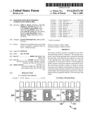
  • 1. 111111 1111111111111111111111111111111111111111111111111111111111111 (12) United States Patent Bream et al. (54) HEATSINK WITH HIGH THERMAL CONDUCTIVITY DIELECTRIC (75) Inventors: Jeffrey L. Bream, Bethlehem, PA (US); Stephen A. Ferranti, Rowlett, TX (US); Madhu Ganesa-Pillai, Dallas, TX (US); Leon Klafter, Allen, TX (US); Alan M. Lyons, New Providence, NJ (US); John Paul Mello, Dallas; Steven J. Vargo, Midlothian, both of TX (US) (73) Assignee: Lucent Technologies Inc., Murray Hill, NJ (US) ( *) Notice: Subject to any disclaimer, the term of this patent is extended or adjusted under 35 U.S.C. 154(b) by 0 days. (21) Appl. No.: 09/252,741 (22) (51) (52) (58) (56) Filed: Feb. 19, 1999 Int. Cl? .............................. HOSK l/18; H05K 1!09; H05K 3/30 U.S. Cl. ......................... 174/260; 174/16.3; 174/252; 361/705; 361/707; 361/708; 165/80.2; 165/185; 165/80.3; 257/707; 257/713; 257/717 Field of Search .................................... 174/260, 16.3, 174/252; 361/708, 707, 704, 705, 719, 720; 165/80.2, 80.3, 185; 257/707, 713, 717 References Cited U.S. PATENT DOCUMENTS 5,146,981 * 9/1992 Samarov .............................. 165/185 r--- - - - - r--... 2l:2!:2': ,..-241 240 r-- '242 ~ '243 US006225571Bl (10) Patent No.: (45) Date of Patent: US 6,225,571 Bl May 1, 2001 5,344,795 * 9/1994 Hashemi et a!. ................ 264/272.15 5,533,256 * 7/1996 Call eta!. .............................. 29/840 5,616,888 * 4/1997 McLaughlin et a!. ............... 174/260 5,757,073 * 5/1998 Hoffmeyer ........................... 257/700 5,931,222 * 8/1999 Toy et a!. ............................ 165/80.3 6,011,299 * 1!2000 Brench ................................. 257/660 6,021,044 * 2/2000 Neville, Jr. et a!. ................. 361!700 6,084,775 * 7/2000 Bartley et a!. ....................... 361!705 6,085,833 * 7/2000 Kimura et a!. ....................... 165/185 6,088,226 * 7/2000 Rearick ................................ 361!704 6,154,369 * 11/2000 Martinez, Jr. et a!. .............. 361/719 * cited by examiner Primary Examiner-Jeffrey Gaffin Assistant Examiner---Ishwar B. Patel (57) ABSTRACT The present invention provides a heatsink for use with a heat-generating electrical component. The heatsink com- prises a spine having opposing sides, cooling fins extending from the spine, and a dielectric layer adhered to at least one of the opposing sides. The dielectric layer has a thermal conductivity of at least about 1 W/m0 C. The heatsink may further comprise a metal layer adhered to the dielectric layer. The metal layer provides a surface to which an electric component can be adhered. The heatsink can further include a heat-generating component adhered to the metal layer. In another aspect, the heat-generating component is a surface- mount electrical component adhered to the metal layer with solder. ;2!:!2 XXl! 16 Claims, 3 Drawing Sheets - - - r - - - - ~140 r 255 rr,~251 250 '~- r1 ~ a!:~r--252 1'-253...._ 'l' 1/ 130 .. 110 "100
  • 2. Prior Mello Patents Master Index Patent Inventors 6225571 Jeffrey L. Bream,Stephen A. Ferranti,Madhu Ganesa-Pillai, Leon Klafter, Alan M. Lyons, John Paul Mello, Steven J. Vargo 6204452 Armando Rodriguez Valadez, JuanDe Dios Concha Malo, BelisarioSanchez Vazquez, Mario Sanchez Mello 6186799 Keith F. Mello 6186059 Frank C. Mello, Jeffrey A. Williams, Kenneth M. Ware 6125682 Michael Rzasa, Keith Mello 5997368 Keith F. Mello, H.Thomas Nelson, GerhardP. Schwebler 5966982 Keith Mello, H.Thomas Nelson 5957733 Keith F. Mello, Raymond G. Lavoie, ChristopherG. Chadbourne, William J. Lasko, Roger H.Hanks 5956604 Sabrina L. Lee,KevinE. Mello, Steven R. Soss, Toh-Ming Lu, ShyamP. Murarka 5942712 Craig S. Mello 5932456 Arlen Van Draanen, StevenMello 5916424 Charles J. Libby, Donald E. Yansen,Gregory J.Athas, Raymond Hill, RussellMello 5910878 Alfred A. Mello, DonaldL. Pearl 5888104 Keith F. Mello, H.Thomas Nelson 5866427 Jack H. Mendelson, Nancy K. Mello, Tak-Ming Chiu 5820904 Frank C. Mello, Roger S. Williams, Jeffrey A. Williams 5778793 Kathryn M. Mello,Matthew M. Semiao 5775313 Douglas T. Bresette, JohnMello,III 5770249 Frank C. Mello, Jeffrey A. Williams, Roger S. Williams 5759072 Richard Chadbourne,KeithMello,GennaroL. Pecora 5681745 PrzemyslawSzafranski, CharleneM. Mello,Takeshi Sano, Kenneth A. Marx, Charles R. Cantor, David L. Kaplan, Cassandra L. Smith 5679533 PrzemyslawSzafranski, CharleneM. Mello,Takeshi Sano, Kenneth A. Marx, Charles R. Cantor, David L. Kaplan, Cassandra L. Smith 5677154 Arlen Van Draanen, StevenMello 5597606 Lee Kramer, Roger S. Williams,Jeffrey A. Williams, Frank C. Mello, DaleV. Miller 5580597 Lee Kramer, Roger S. Williams,Frank C. Mello, Jeffrey A. Williams, DaleV. Miller 5552406 Jack H. Mendelson, Nancy K. Mello 5542234 Ihor Wyslotsky, Frank C. Mello 5355990 John T. Pitts, Ary O. Mello,Gerald E. Johnson 5287265 Richard A. Hall, Gary J. Mello 5284237 Ary O. Mello, GeraldE. Johnson,Mukunda Pramanik 5226522 Gerald E. Johnson, Mukunda B. Pramanik, Ary O. Mello 5199302 Frank P. Mello 5178559 Craig S. Mello 5156252 Ary O. Mello, GeraldE. Johnson,Arthur McClement 5106670 Ihor Wyslotsky, Frank C. Mello 5092215 William Mello, John Hendrickson 5083700 Frank C. Mello, Jan Gullett 5075341 Jack H. Mendelson, Nancy K. Mello 5054266 Frank C. Mello, Ihor Wyslotsky 4955983 DanielC. Meess,BobbyJ. Jones, Raymond M. Mello, Thomas G. Weiss, Jr., James B. Wright 4934767 Hazen L. Hoyt,III,JonC. Goldman, WilliamR. Mello 4830261 Mark D. Mello, StevenC. Iemma,Ray M. Hill, Charles W. Miller, Jr.,Louis G. Blais, Carl E. Andersen,J. TerenceFeeley 4825088 Balakrishnan R. Nair, RaymondV. Richardson, RaymondM. Mello 4728246 William R. Mello 4722659 Hazen L. Hoyt III, JohnD. Sanders, Jon C.Goldman, WilliamR. Mello 4504824 William R. Mello 4250591 Frank A. Mello 4236654 Frank A. Mello
  • 3. 4098448 Albert M. Sciaky, WilliamR. Mello 4046169 Louis P. Pollono, RaymondM. Mello 3968882 Fabio Mello
  • 4. U.S. Patent r-- r-- -....... :x:l!::X 240 ---. nX May 1, 2001 100 " 111 140 145 150 170 r-- - ~,---241 r--- 242 1'-.243 Sheet 1 of 3 FIG. 1 120 FIG. 2 r-- - 110 112 130 - US 6,225,571 Bl r-- - - r-- -- ~ 255 rril~,---251 250-- ,f-~ r.,~ ~f~'--252txxx 140 __ ,. ~'-253 / ..130 110 "-too
  • 5. U.S. Patent May 1, 2001 FIG. 3A 240 """ Sheet 2 of 3 r38 : 343I I :..-- 1 I I : 243 I I I I I US 6,225,571 Bl 241 242 r- - ..... ~--~-~--~-~- I ~ '•342 I __________ j ~38 FIG. 3B 13o ,________,y 140 350 243 242 150
  • 6. U.S. Patent May 1, 2001 Sheet 3 of 3 US 6,225,571 Bl FIG. 4 400 (START 410 450 '- _./ HEATSINK ETCH METAL SPINE SELECTION LAYER 420 460 '- _./ PLACE SCREEN PRINT DIELECTRIC LAYER SOLDER 430 470 '- PLACE ELECTRONIC_./PLACE METAL LAYER DEVICES 440 480 '- vHEAT AND REFLOW PRESSURE CYCLE SOLDER 490 END
  • 7. US 6,225,571 Bl 1 HEATSINK WITH HIGH THERMAL CONDUCTIVITY DIELECTRIC TECHNICAL FIELD OF THE INVENTION 2 Accordingly, what is needed in the art is a heatsink with a low thermal impedance between the electronic component and the body of the heatsink while maintaining good dielec- tric characteristics and eliminating mechanical fasteners. The present invention is directed, in general, to a heatsink 5 and, more specifically, to a heatsink having an insulating dielectric with a high thermal conductivity. SUMMARY OF THE INVENTION To address the above-discussed deficiencies of the prior art, the present invention provides a heatsink for use with a heat-generating electrical component. The heatsink com-BACKGROUND OF THE INVENTION Because of the ever increasing demand placed on elec- trical components, in general, electronic designers need to be able to pack higher powered components closer together in ever smaller spaces. More power in less space translates to higher watt densities, and therefore, increased heat gen- eration. As temperatures rise, the reliability and functionality of electronic components are impaired dramatically. Expe- rience has shown that more than 50 percent of electronic failures are the result of thermal problems. Traditionally, heatsinks are used to move heat from components generat- ing the heat to an area where the heat can be dissipated to the atmosphere or adequate ventilation can be provided to the heatsink. Conventional heatsinks use some type of mechanical method to attach the heat-generating component to the heatsink. The most common methods are: adhesives, spring clamping devices, or hold-down brackets with a mechanical fastener such as a machine screw. These methods generally require an assembler to make the mechanical attachment of the component to the heatsink. Heat-generating electronic devices need to be electrically isolated from the heatsink in many cases. Currently the devices are electrically isolated by a thermal interface pad, which results in a substantial thermal contact resistance. Typically, in a stamped heatsink assembly, the presence of the thermal interface pad can contribute up to 50 percent of the overall thermal resistance, even in the best designs. However, heat generating devices may be directly mounted 10 prises a spine having opposing sides, cooling fins extending from the spine, and a dielectric layer adhered to at least one of the opposing sides. The dielectric layer has a thermal conductivity of at least about 1 W/m0 C. In one embodiment, the heatsink further comprises a metal layer adhered to the 15 exposed surface of the dielectric layer. The metal layer is preferably adhered to exposed surface of the dielectric layer without the use of conventional adhesives that are typically used to adhere electrical components to heatsinks. Thus, the problems associated with the use of such conventional 20 adhesives are avoided. Once attached to the dielectric layer, the metal layer provides a surface to which an electric component can be attached. In another aspect of this embodiment, the heatsink further includes a heat-generating component adhered or attached to the metal layer. In a 25 particularly advantageous embodiment, the heat-generating component is a surface-mount electrical component that is adhered to the metal layer with solder. In another embodiment, the metal layer is patterned to form concentric patterns on the dielectric layer to provide a 30 mounting location for electrical components having mount- ing footprints of different sizes. These concentric patterns can be used as a self-aligning mark for easily placing or positioning the electrical components on the metal layer. In one aspect of this embodiment, the metal layer forms at least 35 three concentric patterns to accommodate any of three different sizes of electrical components. In a particularly advantageous embodiment, the concentric patterns provide a self-aligning pattern for adhering a surface-mountable elec- trical component thereon during a soldering process. on the heatsink. In at least one conventional approach, the entire heatsink is covered with a dielectric material prior to mounting the device on an intervening metal foil layer. By 40 covering unnecessary areas of the heatsink with the dielectric, the thermal efficiency of forced convection cool- ing is significantly reduced. When the device is surface mounted, the contact resistance is very low, because of the metal to metal bond between the tab of the device and the metal foil substrate. In another embodiment, the electrical component has electrical leads extending therefrom with each of the elec- trical leads configured to be received in a corresponding contact opening within a printed wiring board. The self- aligning pattern aligns each of the electrical leads with one 45 of the corresponding contact openings, respectively. In yet another embodiment, the heatsink further includes a heat-generating component adhered to the dielectric layer. The dielectric layer, in particularly advantageous embodiments, comprises material with a thermal conductiv- There are additional thermal transfer inefficiencies asso- ciated with the way in which components are conventionally attached to the heatsink. Although the component surface and the mating surface appear to be smooth, under adequate magnification it can be shown that they are actually rough. When a heatsink is mated with a heat-generating device by a mechanical means such as a spring clamp or hold-down bracket, microscopic peaks in the surface of the component ride upon corresponding microscopic peaks of the heatsink. Therefore, the two surfaces are not in the close physical proximity that fosters good heat transference by conduction. Of course, this poor thermal conductivity results in higher device temperatures which, in turn, lead to device failures. Alternatively, adhesives are often used to adhere the elec- trical component to the heatsink; however, these conven- tional adhesives also bring disadvantages. For example, while these adhesives often have good dielectric characteristics, they are not good thermal conductors, or, if they are good thermal conductors, they tend to have poor dielectric characteristics. Thus, these present day adhesives do have undesirable characteristics. 50 ity ranging from about 2 W/m0 C. to about 15 W/m0 C. The dielectric layers may be adhered to each of the opposing sides with a metal layer being adhered to each of the dielectric layers. In one aspect of this particular embodiment, the heatsink has an electrical component 55 adhered to each of the metal layers. The foregoing has outlined, rather broadly, preferred and alternative features of the present invention so that those skilled in the art may better understand the detailed descrip- tion of the invention that follows. Additional features of the 60 invention will be described hereinafter that form the subject of the claims of the invention. Those skilled in the art should appreciate that they can readily use the disclosed conception and specific embodiment as a basis for designing or modi- fying other structures for carrying out the same purposes of 65 the present invention. Those skilled in the art should also realize that such equivalent constructions do not depart from the spirit and scope of the invention in its broadest form.
  • 8. US 6,225,571 Bl 3 BRIEF DESCRIPTION OF THE DRAWINGS For a more complete understanding of the present invention, reference is now made to the following descrip- tions taken in conjunction with the accompanying drawings, in which: FIG. 1 illustrates an end elevational view of one embodi- ment of a heatsink constructed according to the principles of the present invention; FIG. 2 illustrates a side view of the heatsink of FIG. 1; FIG. 3A illustrates a plan view of three standard sizes of components affixed to the concentric patterns of the heatsink of FIG. 1; FIG. 3B illustrates a partial sectional view of a heat- generating device and heatsink of FIG. 3A along line 3B-3B; and FIG. 4 illustrates a flow diagram showing the various operations conducted during manufacture and assembly of the heatsink and components illustrated in FIGS. 1 and 2. DETAILED DESCRIPTION Referring initially to FIG. 1, illustrated is an end eleva- tiona! view of one embodiment of a heatsink constructed according to the principles of the present invention. A heatsink, generally designated 100, comprises a spine 110, cooling fins 120, a dielectric layer 130, and a metal layer 140. Also shown are heat-generating devices 150, 160, with contact leads 152, 162, through contact openings 171 in a printed wiring board (PWB) 170. The spine 110 may be constructed of any suitable material, most commonly aluminum, copper, steel or other excellent thermal conducting materials. In an alternative embodiment, the spine 110 may be of aluminum and com- prise surfaces 111, 112 that have been treated to improve adhesion between the spine 110 and the dielectric layer 130. This surface treatment may be accomplished by chemical cleaning, grit blasting, etching, or anodizing. Adhesion is an important issue in this application due to the CTE (coefficient of thermal expansion) mismatch between the aluminum spine 110 (24 ppm) and the copper-based metal layer 140 (17 ppm). One who is skilled in the art will recognize that because of the different CTEs, differing peel stresses will occur during thermal cycling at the aluminum spine 110 and dielectric layer 130 junction than at the metal layer 140 and the dielectric layer 130 junction. The dura- bility of the adhesive bond strength increases as the selected surface treatment process moves from cleaning to grit blast- ing to etching to anodization. For an ac-dc rectifier appli- cation where the module typically runs warm and in an indoor environment, grit blasting the aluminum should be sufficient to achieve good reliability. However, grit blasting the surface, although an inexpensive process, leaves the aluminum fins untreated and subject to oxidation and cor- rosion. A high purity aluminum alloy, which is preferably >99% pure aluminum, is inherently corrosion resistant. Other less pure alloys would necessitate a surface treatment to inhibit corrosion. Any anodization process will both improve adhesion and prevent corrosion. Another group of aluminum surface treatments com- monly used to prevent corrosion are called conversion coatings. Among commercially available conversion coat- ings are IrriditeTM and AlodineTM. Most are chromate-based coatings; however, to avoid the use of carcinogenic chro- mium solutions, non-chromate based conversions coatings, such as Alodine 2000, Alodine 300+Deoxylyte® and Ala- dine™ 5200, are now available and may be used in place of 4 the chromate-based conversion coatings. All of these coat- ings have been shown to protect aluminum surfaces from corroswn. Therefore, in a specific embodiment, the spine 110 may be 5 anodized aluminum. Anodizing is a low-cost metal treat- ment that improves chemical resistance of the aluminum to acidic solutions, improves bond strength of the dielectric layer 130, and provides an added layer of dielectric isolation between the devices 150, 160 and the spine 110. The cooling 10 fins 120 may be of any design that presents the desired surface area for heat dissipation. In the illustrated embodiment, the dielectric layer 130 and metal layer 140 have been applied to the surface of opposing sides 111, 112 of the spine 110. One who is skilled in the art will recognize 15 that the heatsink may also be constructed with a dielectric layer 130 and metal layer 140 on only one side. The dielectric layer 130 preferably has a thermal conductivity of at least about 1 W/m0 C. In an alternative embodiment, however, the dielectric layer 130 may have a thermal con- 20 ductivity ranging from about 2 W/m0 C. to about 15 W/m0 C. For example, one dielectric material presently available is T-preg™, which has a thermal conductivity of about 8 W/m0 C. It is also highly desirable that the dielectric layer 130 have good dielectric characteristics as well. For example, it is 25 desirable that the dielectric layer 130 have a dielectric strength of about 2500 V. The heat-generating devices 150, 160 may be surface mounted to an exposed surface 140a of the metal layer 140 by a solder layer 145. When molten, solder fills the microscopic voids between the irregular 30 surfaces of the metal layer 140 and the heat-generating device 150, thereby improving surface-to-surface thermal transmission. In this particular embodiment, the use of solder in place of the conventional adhesion systems dis- cussed above substantially improves the thermal conduc- 35 tance between the metal layer 140 and the heat-generating device 150 due to the molten solder's ability to fill the microscopic voids. Referring now to FIG. 2, illustrated is a side view of the heatsink of FIG. 1. Shown in this view of the heatsink 100 40 are alternative forms of concentric patterns 240, 250, formed from the metal layer 140 that is adhered to the spine 110. To form concentric pattern 240, the metal layer 140 may be formed as a continuous layer on the dielectric layer 130. Of course, the number of sites 240, 250 are dependent upon the 45 number and sizes of components. The metal layer 140 may then be photolithographically etched using conventional methods to form pattern 240 with dielectric areas 232, 233 exposed between adjacent concentric metallic patterns 241, 242, 243. Photolithography enables the formation of all 50 types of circuit designs, including those with small, isolated traces. Photolithography also enables some circuitry to be moved from the PWB to the heatsink, saving useful area on the PWB. However, in the photolithography process, as one who is skilled in the art will understand, acid is used to etch 55 away unprotected copper areas of the metal layer 140. In this process, exposed aluminum of the heatsink is subjected to an acidic environment that will rapidly erode it. Thus, the key to effectively implementing photolithography is to protect exposed aluminum surfaces prior to copper layer 140 lami- 60 nation. This can be achieved by anodizing the aluminum as described above, and sealing the surface with a combination of nickel acetate and chromic acid. Alternatively, the alu- minum may be sealed with steam, triethanolamine, sodium silicate, etc. A discussion of sealing may be found in The 65 Surface Treatment and Finishing of Aluminum and Its Alloys, 5th Ed., Vol. 2, Chapter 11, "Sealing Anodic Oxide Coatings," pg. 773-856, incorporated herein by reference.
  • 9. US 6,225,571 Bl 5 However, it may be desirable to form the metal layer 140 separately as concentric pattern 250 comprising patterns 251, 252, 253 and then affix them to the dielectric layer 130. Concentric patterns 240 and 250 differ by the absence or presence of interconnects 255. The interconnects 255 main- 5 tain precise spacing between patterns 251, 252, and 253 during the application of concentric pattern 250 to the dielectric layer 130. This approach is commonly achieved by stamping the patterns 250 from a sheet with a lead frame (not shown). One who is skilled in the art is familiar with 10 lead frame technology. As described above, concentric pat- tern 240 is formed by etching away the metal layer 140 from areas 232, 233, the interconnects 255 are not required. Of course, the number of concentric patterns 240, 250 that may be formed on the heatsink is dependent upon the size and 15 number of components and the size of the heatsink. For example, a three inch long heatsink may have up to three mounting sites on one side for components with TO 218, TO 220 and TO 247 package sizes. Referring now to FIG. 3A with continuing reference to 20 FIG. 1, illustrated is a plan view of three standard sizes of components affixed to the concentric patterns of the heatsink of FIG. 1. In the illustrated embodiment, the essentially- rectilinear, concentric patterns 240, 250 are sized to accept surface mounting of three standard sizes 341, 342, 343 25 (dashed lines) of electrical components. Each size fits pre- cisely to a surface mounting area offered by one of the patterns 241, 242, 243, respectively. Of course, the number of concentric patterns 241, 242, 243, may be as few as two or as many as the physical area allows. Similarly, a single 30 pattern may also be formed. One who is skilled in the art will understand that other standard sizes of electrical components may likewise be nested in concentric patterns. When heat- generating devices 150, 160 are soldered to the patterned metal layer 140, the devices 150, 160 self-align with the 35 appropriate size pattern 241, 242, or 243 during the time that the solder 145 is molten. The self-alignment property of the surface mount process is well known to those who are skilled in the art. Thus, precision placement of the concentric patterns 240, 250 on the dielectric layer 130 assures that 40 contact leads 152 or 162 are properly positioned to coop- eratively engage contact openings 171 in the printed wiring board 170. One who is skilled in the art will recognize that while the illustrated embodiment incorporates wiring through the printed wiring board 170, the present invention 45 is also applicable to surface mount technology wherein the leads 152, 162 may be adapted to cooperate with mating pads (not shown) on the printed wiring board 170. Referring now to FIG. 3B, illustrated is a partial sectional view of a heat-generating device and heatsink of FIG. 3A 50 along line 3B-3B. As can be seen, the solder layer 145 under the heat-generating device 150 conforms to a surface- mount face 350 of the heat-generating device 150 and the pattern 242. Also shown for clarity are patterns 241 and 243. Because the solder 145 adheres only to the thin metal layer 55 140 and not to the dielectric layer 130, the surface tension of the solder 145 during its molten state automatically aligns the device 150 to the pattern 242. Therefore each size of device 150, 160 automatically aligns to the appropriate pattern 241, 242, or 243. Turning now to FIG. 4 with continuing reference to FIGS. 60 1 and 2, there is illustrated a flow diagram showing the various operations conducted during manufacture and assembly of one embodiment of the heatsink and compo- nents illustrated in FIGS. 1 and 2. As shown, the process 65 starts at 400. At 410, a heatsink spine 110 is selected. In a specific embodiment, the spine 110 may be a coupon of 6 anodized and sealed aluminum alloy 1100 H14, having dimensions of 2"x3"x0.25". The dielectric layer 130 is placed on a side 111 of the spine 110 at 420. The dielectric layer 130 may be, for example of T-Preg™, about one inch width placed along a long edge of the heatsink spine 110. Of course, one who is skilled in the art will readily observe that other similar materials may also be used. At 430, the metal layer 140 is placed on the dielectric layer 130. The metal layer 140 may be copper foil of about one inch width. The assembly 100 is subjected to heat of 170° C. and pressure of 200 psi for 45 minutes to affix the metal layer 140 and dielectric layer 130 to the spine 110 at 440. As previously discussed, an additional dielectric layer 130 and an addi- tional metal layer 140 may be affixed, if required, to the reverse side 112 of the spine 110 by appropriately repeating 420, 430 before 440. Of course, as one who is skilled in the art will readily observe, the metal layers 140 may be laminated simultaneously, which would be preferred if the geometry permits. At 450, the metal layer 140 is lithographically defined and conventionally etched to form concentric patterns 240. In a particularly advantageous embodiment, the copper metal layer 140 is etched to remove the copper 140 a distance of 0.12" from the edge of the dielectric layer 130. It has been found that the dielectric layer 140 thickness tapers toward its edges from a central thickness of about 0.008" to 0.009" down to a thickness of about 0.002" over the peripheral 0.12". Thus, removing the copper metal layer 140 over the peripheral 0.12" insures planarity of the copper foil140 and avoids insufficient dielectric thickness between the device and the spine 110. Solder is then screen printed to selected patterns 241, 242, 243 on the heatsink 100 at 460. At 470, heat-generating devices 150, 160 are placed over selected patterns 241,242, 243 of the heatsink 100. The heatsink 100 and the heat-generating devices 150, 160 are subjected to a heating cycle to refiow the solder 145 at 480. The process ends at 490. Thus, a high thermal conductivity dielectric has been interposed between a heatsink spine 110 and a con- ductive metal layer 140 thereby eliminating conventional mechanical fasteners. This provides: improved dielectric strength, enables conventional surface-mount technology assembly and repair processes, and accurately locates com- ponents for subsequent mounting to a PWB. Photolithogra- phy has the additional advantage of enabling some circuitry to be moved from the PWB onto the heatsink, thus freeing area of the PWB. Although the present invention has been described in detail, those skilled in the art should understand that they can make various changes, substitutions and alterations herein without departing from the spirit and scope of the invention in its broadest form. What is claimed is: 1. For use with a heat-generating electrical component, a heatsink, comprising: a spine having opposing sides; cooling fins extending from said spine; a dielectric layer adhered to at least one of said opposing sides; and a metal layer adhered to said dielectric layer, said metal layer including concentric patterns on said dielectric layer to provide mounting locations for electrical com- ponents having mounting footprints of different sizes. 2. The heatsink as recited in claim 1 further comprising a heat-generating component adhered to said metal layer. 3. The heatsink as recited in claim 3 wherein said heat- generating component is a surface-mount electrical compo- nent adhered to said metal layer with solder.
  • 10. US 6,225,571 Bl 7 4. The heatsink as recited in claim 1 wherein said metal layer forms at least two concentric patterns. 8 5. The heatsink as recited in claim 1 wherein each of said concentric patterns provides a self-aligning pattern for adhering a surface-mountable electrical component thereon 5 during a soldering process. a metal layer adhered to said dielectric layer, said metal layer including concentric patterns on said dielectric layer to provide self-aligning mounting locations for electrical components having mounting footprints of different sizes; and a heat generating electrical component adhered to said metal layer, said electrical component having elec- trical leads extending therefrom by which said elec- 6. The heatsink as recited in claim 5 wherein said elec- trical component has electrical leads extending therefrom with each of said electrical leads configured to be received in a corresponding contact opening within a printed wiring 10 board, said self-aligning pattern aligning each of said elec- trical leads with one of said corresponding contact openings, respectively. trical component can be electrically connected to said printed wiring board. 12. The printed wiring board as recited in claim 11 wherein said printed wiring board includes contact openings formed therein and each of said electrical leads is configured to be received in a corresponding one of said contact7. The heatsink as recited in claim 1 further comprising a heat-generating component adhered to said dielectric layer. 8. The heatsink as recited in claim 1 wherein a thermal conductivity of said dielectric layer ranges from about 1 W/m0 C. to about 15 W/m0 C. 9. The heatsink as recited in claim 1 further comprising dielectric layers adhered to each of said opposing sides and a metal layer adhered to each of said dielectric layers. 10. The heatsink as recited in claim 9 further comprising an electrical component adhered to each of said metal layers. 11. A printed wiring board, comprising: electrical components mounted on and electrically con- nected to said printed wiring board; and a heatsink mounted on said printed wiring board and including: a spine having opposing sides; cooling fins extending from said spine; a dielectric layer adhered to at least one of said oppos- ing sides; 15 openings, said self-aligning pattern aligning each of said electrical leads with said one of said corresponding contact openings, respectively. 13. The printed wiring board as recited in claim 11 wherein said heat-generating component is a surface-mount 20 electrical component adhered to said metal layer with solder. 14. The printed wiring board as recited in claim 11 wherein said metal layer forms at least two concentric patterns. 15. The printed wiring board as recited in claim 11 25 wherein each of said concentric patterns provides a self- aligning pattern for aligning said electrical leads to an electrical contact point on said printed wiring board. 16. The printed wiring board as recited in claim 11 wherein a thermal conductivity of said dielectric layer 30 ranges from about 1 W/m0 C. to about 15 W/m0 C. * * * * *