Datasheet of TB6819AFG
•
0 recomendaciones•380 vistas

This document summarizes the features and operation of the TB6819AFG critical conduction mode power factor correction (PFC) controller IC. It contains an 8-pin SOP package and operates from 10-25V while providing a maximum current of 1A. It uses various protection circuits and zero current detection to control an external switching MOSFET in a boost converter configuration to shape the input current and regulate the output voltage. The IC aims to achieve a power factor close to 1 while providing overvoltage and undervoltage protections.

Recomendados
Más contenido relacionado
La actualidad más candente
La actualidad más candente (18)
Destacado
Similar a Datasheet of TB6819AFG
Similar a Datasheet of TB6819AFG (20)
Más de Tsuyoshi Horigome
Más de Tsuyoshi Horigome (20)
Último
Último (20)
Datasheet of TB6819AFG
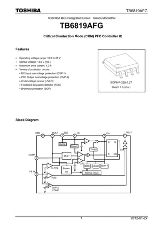
- 1. TB6819AFG TOSHIBA BiCD Integrated Circuit Silicon Monolithic TB6819AFG Critical Conduction Mode (CRM) PFC Controller IC Features • Operating voltage range: 10.0 to 25 V • Startup voltage: 12.0 V (typ.) • Maximum drive current: 1.0 A • Variety of protection circuits • DC Input overvoltage protection (OVP-1) • PFC Output overvoltage protection (OVP-2) • Undervoltage lockout (UVLO) SOP8-P-225-1.27 • Feedback-loop open detector (FOD) Weight: 0.1 g (typ.) • Brownout protection (BOP) Block Diagram GND MULT ZCD IS Vcc POUT 6 3 5 4 8 7 - + S Q Clamp Timer2 Timer1 + R QN COMP - MULT 2 - + - LLP BIAS UVLO OVP-1 + E-Amp . Brown- FB IN out Internal circuit 1 + - FOD - + OVP-2 COMP. 1 2012-01-27
- 2. TB6819AFG Absolute Maximum Ratings (Ta=25°C) Characteristics Symbol Rating Unit Supply voltage Vccmax 25.0 V Maximum input voltage on all pins Vinmax (Note 3) V Minimum input voltage on all pins Vinmin GND - 0.3 V Power dissipation 1 (Note 1) PDmax 650 mW Operating ambient temperature (Note 2) Topr -40 to 85 °C Junction temperature Tj 150 °C Storage temperature Tstg -55 to 150 °C Note 1: The rated power dissipation should be decreased by 5.2mW/°C at above Ta = 25°C ambient. Note 2: Functional operation is guaranteed over the specified temperature range. Note 3: See the table below Maximum Input Voltage Pin No. Pin Name Unit (Rating) 1 FB IN 5.0 2 COMP 5.0 3 MULT 5.0 4 IS 5.0 V 5 ZCD 7.0 6 GND ― 7 POUT Do not apply any voltage. 8 Vcc 25.0 Pin Assignments 1: FB IN 1 8 2: COMP 2 7 3: MULT 4: IS 3 6 5: ZCD 6: GND 4 5 7: POUT 8: Vcc 2 2012-01-27
- 3. TB6819AFG Pin Function No. Pin Name Functional Description Output voltage feedback pin. This is the input of the error amplifier (E-Amp), OVP-2 and FOD. The PFC output voltage should be resistively divided down and applied to this pin. The error amplifier reference voltage is set to 2.51V (typ.). For other features, see the following. 1. Overvoltage protection on the PFC output (OVP-2) 1 FB IN If the PFC output voltage increases and this pin voltage exceeds 2.69V, the POUT (pin 7) output is forced to Low. The POUT pin will then be enabled again when this pin voltage falls below 2.51V. 2. Feedback-loop open detection (FOD) If this pin voltage falls below 0.25V because of error conditions such as a Feedback–loop open, the POUT (pin 7) output is forced to Low. The POUT pin will then be enabled again when this pin voltage reaches 0.5V. Error amplifier output. 2 COMP An external filter is required to keep the open loop gain below 0dB at the frequency twice the AC input frequency that is superimposed on the PFC output. This external filter must be designed to provide enough phase margins. Detection pin for a full-wave rectified AC voltage waveform. This pin is the input of the multiplier and BOP circuit. The full-wave rectified voltage is resistively divided and connected to this pin. The full-wave rectified voltage applied to this pin is internally multiplied to serve as a reference 3 MULT signal for the PFC operation. If the MULT voltage is below 0.75V, the BOP is activated and the TB6819AFG does not enter Standby mode. After the TB6819AFG is started, it stops its operation and enters Standby mode if the MULT voltage falls below 0.55V and peak voltage remains below 0.75V for 100ms. Input pin for the current detection comparator. If the IS voltage exceeds the multiplier output voltage, which is the IS comparator reference voltage, the RS flip-flop is reset. Too high a multiplier 4 IS output voltage causes an external switch to fail to switch off. To avoid this, the upper limit of the IS comparator reference voltage is clamped to 1.7V. Zero current detection pin for an external transformer. The zero-current detector senses an inductor current via the auxiliary winding of the coil and sets the RS flip-flop when the current reaches zero. 5 ZCD Since the voltage of auxiliary winding varies significantly, the ZCD pin has an internal clamp circuit. If the inductor current does not reach zero for 200μs (typ.) while the TB6819AFG is running, the Timer1 restart timer output sets the RS flip-flop and restarts the switching. 6 GND Ground pin. 7 POUT Switching pulse output supplied to the FET switch. Supply voltage input pin for the TB6819AFG operation. The operating voltage ranges from 10V 8 Vcc (min.) to 25V (max.). Owing to the UVLO feature, the TB6819AFG is turned off when Vcc falls below 9.5V. The TB6819AFG is turned on again when Vcc reaches 12V. ・Notes when the protection circuits are working The internal circuit works as shown in the following table when the protectors are operating. Except for TSD, the output of pin 7 is kept at a low level in order to shut down outer FET. Only in the case of TSD is the output of pin 7 is kept floating. It is necessary to connect the pull down resistor to save outer FET when TSD works. TSD is accorded top priority. Even if the other protector is working, pin 7 floats if the IC temperature exceeds 175°C (typ.). Protector Remarks (typ.) Internal circuit Pin 7 output OVP-2 FBIN ≥ Verr (2.51V) + 180mV Working L FOD FBIN ≤ 0.5V Working L UVLO Vcc ≤ 9.5V Standby L Brown out MULT ≤ 0.75V Standby L TSD Chip temperature ≥ 175°C Standby Floating 3 2012-01-27
- 4. TB6819AFG Electrical Characteristics (unless otherwise specified, Vcc = 15V, Ta = 25°C) Characteristics Symbol Remarks Min. Typ. Max. Unit Supply voltage range Vcc 10 15 25 V Current consumption Icc 75kHz, 1000pF ― 4 6.5 mA Startup current Istart At startup ― 72.5 99 μA VoH Output load current: 100mA Vcc-2.0 ― ― Output pulse voltage V VoL Output load current: 100mA ― ― 0.4 Output pulse rise time TRPF Load: 10Ω, 1000pF ― 25 50 ns Output pulse fall time TSPF Load: 10Ω, 1000pF ― 10 30 ns Input OVP voltage VOVP-1 Self-limiting 25 27.5 31.5 V Threshold voltage (disables POUT) Verr+0.12 Verr+0.18 Verr+0.24 V Output OVP voltage VOVP-2 Recovery threshold Verr-0.05 Verr Verr+0.05 V Threshold voltage (disables POUT) 0.20 0.25 0.30 V FOD trip threshold voltage VFOD Hysteresis 180 250 300 mV Shutdown threshold 8.8 9.5 10.2 UVLO trip threshold voltage VUVLO V Recovery threshold 11.5 12 12.5 Negative-going threshold voltage 1.2 1.4 1.6 V ZCD trip threshold voltage VZCD Hysteresis 150 300 400 mV Upper limit: 3mA 4 5.8 6.3 ZCD clamp voltage VZCDP V Lower limit: -3mA 0.15 0.5 0.9 E-Amp reference voltage Verr 2.46 2.51 2.56 V E-Amp mutual conductance gm 55 90 135 μS Ie Source ― -1 ― mA Maximum E-Amp current source Ie sink Sink ― 1 ― mA Output voltage compensation under light-load LLP trip threshold voltage VLLP 1.8 1.9 2.0 V conditions IS pin reference voltage Vis Upper limit of the IS reference voltage 1.55 1.7 1.9 V Including the RC time constant for noise IS rise time ti 210 350 550 ns filtering Restart time t res Timer1 60 200 400 μs FB IN input current IFBIN FB IN = Open, sink current -1 ― 1 μA FOD response time tFOD ― ― 1.5 μs Output OVP response time tOVP-2 ― ― 1.5 μs Vqu Upper 2.55 2.65 2.80 V Quick startup voltage VqL Lower 2.1 2.2 2.3 V MULT input current IMULT -0.1 ― 0.1 μA GMULT×(COMP-2.5) ×MULT = IS MULT gain GMULT 0.35 0.5 0.65 ― COMP=3.5V MULT=2V-1V VLM Maximum MULT input voltage(Lower limit: 0V) 3.0 3.5 ― V MULT input linear operation range Maximum COMP input voltage VLC 3.5 4.0 ― V (Lower limit: Verr) Positive-going threshold voltage (starts the IC) 0.71 0.75 0.79 V Brownout threshold voltage Vb Hysteresis 0.145 0.2 0.275 V Brownout turn-on delay tb Timer3 50 100 200 ms Designed values are indicated in following table, these are not tested at the shipping. Id Source (Reference value) ― 0.5 ― A Maximum POUT current source Id sink Sink (Reference value) ― 1.0 ― A RC time constant for noise τIS Timer2, 40kΩ / 5pF (Reference value) ― 200 ― ns filtering Thermal shutdown Threshold temperature (Reference value) 150 175 ― °C TSD threshold Hysteresis (Reference value) ― 25 ― °C 4 2012-01-27
- 5. TB6819AFG Principle of Operation I-in PFC OUT AC IN L1 V1 I1 C-in V2 Switch L2 GND MULT ZCD IS Vcc POUT 6 3 5 4 8 7 GND ZCD-COMP - + S Q Clamp Timer2 Timer1 + I-COMP COMP R QN MULT - 2 - + - LLP + BIAS UVLO OVP-1 E-Amp Brownout FB IN Internal circuit 1 + - FOD - + OVP-2 COMP (1) Boost Converter Operation 1. Switch: ON The L1 current increases. PULSE 2. The L1 current reaches the I-COMP reference OUT current. RS flip-flop is reset. V1 POUT toggles. Switch goes off. I1 V1 toggles High. V2 toggles High. 3. The L1 current decreases to zero. The V1 and V2 voltages decrease rapidly. V2 4. The V2 voltage falls below the ZCD-COMP reference voltage (1.4V). I-COMP ZCD-COMP goes High. OUT RS flip-flop is set. Switch goes on (Back to ZCD-COMP step 1.) OUT ① 1 ② 2 ③④ 3 4 I-in waveform: Ripple-current filtering using a capacitor C-in I-in波形:コンデンサC-inによってリプル除去 I1 waveform I1波形 (2) Power Factor Correction (Critical Conduction Mode) a) Step 2 causes the I-COMP reference current signal to form a sinusoidal waveform. b) An envelope of the L1 current that flows upon resetting the RS flip-flop to turn the Switch off forms a sinusoidal waveform. I-in,I1波形 Waveforms of I-in and I1 5 2012-01-27
- 6. TB6819AFG Functional Description (1) Error Amplifier (E-Amp) This is an error amplifier for regulating the output voltage to be constant. The TB6819AFG internally generates a reference voltage of 2.51V (typ.). If the E-Amp output includes the harmonics twice as large as the AC input frequency, the E-Amp system becomes unstable. To avoid this, a filter with a cut-off frequency (fc) of about 20Hz should be externally connected to the E-Amp output for eliminating harmonics. (2) DC Input Overvoltage Protection (OVP-1) This circuit protects the internal circuit from a sudden rise of the Vcc voltage in any event. The OVP-1 incorporates a 27.5V (typ.) voltage limiter. (3) PFC Output Overvoltage Protection (OVP-2) This circuit forces the POUT output to Low if the FBIN voltage exceeds 2.69V (typ.) due to the PFC voltage rise in any event. The POUT output will be enabled again when the FBIN voltage falls below 2.51V (typ.). (4) Under Voltage Lockout (UVLO) This circuit disables the internal circuit if the Vcc voltage falls below 9.5V (typ.). Once the internal circuit is disabled, it will then be enabled when Vcc reaches 12V (typ.). (5) Feedback-Loop Open Detector (FOD) The POUT output is forced to Low if the FBIN voltage falls below 0.25V (typ.) because of error conditions such as a feedback–loop open. The POUT output will be enabled again when the FB IN voltage reaches 0.5V (typ.). (6) Thermal Shutdown (TSD) This circuit disables the internal circuit if the chip temperature exceeds 175°C (typ.). The internal circuit will be enabled again when the chip temperature falls below 150°C (typ.). (7) Light-Load Power Control (LLP) This function prevents the PFC output voltage from getting too high during no-load and light-load operations. If an offset voltage is present at the multiplier output, the PFC output voltage might increase abnormally. To avoid this, this feature resets the RS flip-flop if the E-Amp output falls below 1.9V (typ.). (8) Restart Timer (Timer1) This is a restart timer. While the TB6819AFG is running, if the inductor current does not reach zero for 200μs (typ.), the Timer1 output sets the RS flip-flop and restarts the switching. (9) Noise Filtering (Timer2) The TB6819AFG has a filter for filtering pulse noises on the current detect pin (IS pin). Timer2 consists of a 40kΩ resistor and a 5pF capacitor. (10) Brownout Protection Brownout protection disables the internal circuit if AC input voltage falls below the predetermined value. This protection circuit operates separately from the other internal circuits and this feature overrides any other features. At start-up, the RS flip-flop is in the reset state disabling the internal circuit. When the voltage applied to the MULT pin reaches 0.75V (typ.), the RS flip-flop is set to enable the internal circuit. Timer3 is programmed to start when a logical-OR result of the operation comparator output and the QN output of the RS flip-flop becomes Low. If the logical-OR result is continuously kept Low for 100ms, Timer3 generates a reset pulse for resetting the RS flip-flop. That is, if the MULT voltage falls below 0.55V and remains below 0.75V for 100ms while the RS flip-flop is set (QN = Low), Timer3 resets the RS flip-flop and puts the TB6819AFG into Standby mode. 3 + S Q - Internal circuit 0.75/0.55 V 5V Timer3 R QN (11) I-COMP Outputs a reset signal RS-FF by typing what was converted to a voltage source current with a resistor of the MOSFET, compared to the output of the MULT. During this operation, Timer2 filters noise signals having short-pulse durations, such as switching noises. If multiplier output voltage is too high, the RS flip-flop will fail to reset. To avoid this, the upper limit of the IS comparator reference voltage is clamped to 1.7V. 6 2012-01-27
- 7. TB6819AFG Typical Performance Curves Current Consumption vs. Temperature Start up Current Consumption vs. Temperature 4.0 110 100 電流(uA) Current (μA) 電流(mA) Current (mA) 90 3.0 80 70 2.0 60 50 1.0 40 -40 -20 0 20 40 60 80 100 -40 -20 0 20 40 60 80 100 Ta(℃) Ta(℃) UVLO vs. Temperature Shut down Start up 10.5 13.0 電圧(V) 10.0 12.5 電圧(V) Voltage (V) Voltage (V) 9.5 12.0 9.0 11.5 11.0 8.5 -40 -20 0 20 40 60 80 100 -40 -20 0 20 40 60 80 100 Ta(℃) Ta(℃) OVP-1 vs. Temperature Error Amplifier Reference Voltage vs. Temperature 31.0 2.60 30.0 電圧(V) Voltage (V) 2.55 Voltage (V) 電圧(V) 29.0 28.0 2.50 27.0 2.45 26.0 2.40 -40 -20 0 20 40 60 80 100 -40 -20 0 20 40 60 80 100 Ta(℃) Ta(℃) Multiplier Input-Output Characteristics (Ta = 25°C) Multiplier Gain vs. Temperature 2.0 0.9 1.8 MULT_IN =3V 0.8 1.6 0.7 MULTMULTI 出力[V] (V) 2.5V ゲイン 2V 1.4 0.6 output voltage Gain 1.5V 1.2 0.5 0.4 1.0 1V 0.3 0.8 0.2 0.75V 0.6 -40 -20 0 20 40 60 80 100 0.4 Ta(℃) 0.2 0.0 2.5 3.0 3.5 4.0 4.5 COMP電圧[V] COMP Voltage (V) 7 2012-01-27
- 8. TB6819AFG ZCD Voltage Clamp vs. Temperature Upper side Lower side 6.0 1.00 5.8 0.80 Voltage (V) 電圧(V) 電圧(V) Voltage (V) 5.6 0.60 5.4 0.40 5.2 0.20 5.0 0.00 -40 -20 0 20 40 60 80 100 -40 -20 0 20 40 60 80 100 Ta(℃) Ta(℃) Timer1 Restart Time vs. Temperature Error Amplifier Conductance vs. Temperature 300 120 250 110 時間(us) 100 gm(uS) 200 Time (μs) gm (μS) 90 150 80 100 70 50 60 0 50 -40 -20 0 20 40 60 80 100 -40 -20 0 20 40 60 80 100 Ta(℃) Ta(℃) Gate-Drive Output Pulse on time vs. Temperature Gate-Drive Output Pulse off time vs. Temperature 50 30 45 25 時間(ns) 時間(ns) Time (ns) Time (ns) 40 20 35 15 30 10 25 5 20 0 -40 -20 0 20 40 60 80 100 -40 -20 0 20 40 60 80 100 Ta(℃) Ta(℃) Brown out threshold Voltage vs. Temperature Start up Hysteresis Voltage vs. Temperature 0.85 0.30 0.80 0.25 電圧(V) Voltage (V) 電圧(V) Voltage (V) 0.75 0.20 0.70 0.15 0.65 0.10 -40 -20 0 20 40 60 80 100 -40 -20 0 20 40 60 80 100 Ta(℃) Ta(℃) 8 2012-01-27
- 9. TB6819AFG Applications Information NTPA73R0LBMB0 D3 RM10A NF1 KBU8K-E4 T1 L1, N1 VOUT LH26-402Y3R0-01 NTC1 AC_IN1 R11a R5a D1 10kΩ 1MΩ L2, N2 F1 CNF1 R14a R3 5A/250V 2.2nF 180kΩ R11b R5b 750kΩ CNF3 10kΩ 1MΩ PFC3819QM Vin 0.22µF R14b Q2 2SC5307 -231K07D-00 R2 85 to 265V 180kΩ 750kΩ CNF2 2.2nF D9 D8 Q1 1N4007 AC_IN2 J2c 1N5245 TK15A60U J1a J1c C1 J1b + 1µF/400V R10 R15 D4 C2 200µF AC_G 1N400 100Ω 450V J2b R8 39kΩ R12a 68kΩ R7 1.5MΩ C7 10Ω R4 10kΩ C4 8pF 1µF TP-Vcc C3 8 5 7 2 R12b 0.47µF J3b 1.5MΩ J2a 1 3 6 4 R6 100Ω J3a C9 C5 47µF + C10 D7 C6 3300pF R13 1N5248 R9a R9b R1 22kΩ 10nF 30V 0.1µF 0.22Ω 0.22Ω 9.53kΩ GND This chapter provides the minimum description including equations and constants as a guide to understand the TB6819AFG demonstration board. These equations and constants should be optimized according to the specifications of actual applications. Please adjust them according to the specifications to achieve required operation. At the same time, make sure that no problem occurs in the various tests, such as end-product, environmental and durability tests. This application circuit is for 400V-200W output. (1) L1 Inductance Since the TB6819AFG operates in CRM mode, the switching frequency fs (Hz) depends on the L1 inductance and input/output conditions. 2 L1 = (Vo - √2 × Vin (min.)) × η × Vin (min) 2 × 100 × fs × Vo × Po Where Vin (min.) (V) is the minimum AC input voltage (effective value), Vo (V) is the output DC voltage, Po (W) is the output power and η (%) is the power efficiency. The fs value should be within the range between the value sufficiently higher than the audible frequency limit of 20kHz and 150kHz, above which an EMI problem can occur. In this application, fs is targeted to be 50kHz. The power efficiency η is assumed to be about 90%, which is not greatly different from that of actual use. The AC input voltage range is assumed to be between 85V and 265V. Thus, the minimum value Vin (min.) is expected to be 85V, and the output power Vo is 400V. Given that Po = 200W, L1 can be calculated as 227μH. In this application, a commercially available inductor of 230μH is used. (2) Auxiliary Winding L2 The auxiliary winding L2 is used to detect the zero inductor current condition of the inductor L1. L2 is also used for delivering a supply voltage to the TB6819AFG. Since the maximum (positive-going) reference voltage for the ZCD comparator is 1.9V, N1/N2 should meet the following condition to properly perform zero current detection using the auxiliary winding L2: N1 / N2 < (Vo - √2 × Vin (max.)) / 1.9 = 14 Where N1 is the number of winding turns of L1, N2 is that of L2 and Vin (max.) (V) is the maximum AC input voltage (265 V). To ensure that the design requirements are met, N1/N2 should preferably be about 10 to allow for design margins. 9 2012-01-27
- 10. TB6819AFG To deliver a supply voltage to the TB6819AFG by using the auxiliary winding L2, N1 / N2 should meet the following condition: Vo / Vcc (max.) < N1 / N2 < Vo / Vcc (min.) Where Vcc (max.) is the maximum IC supply voltage and Vcc (min.) is its minimum value. To achieve the supply voltage range of 10 to 25 V by only using L2 while obtaining Vo = 400V on the L1 side, N1 / N2 can be calculated as: 400 / 25 < N1 / N2 < 400 / 10. That is, N1 / N2 should be within the range from 16 to 40. However, an inductor of N1 / N2 = 10 is used to achieve proper IC operation. Therefore, an external circuit is required to step down the supply voltage so that it is within the proper range and also for its stabilization. In this application, external circuitry for obtaining the IC supply voltage from the auxiliary winding L2 can be configured in one of the following two ways. These two circuits are different in the block for starting up the IC, while remaining the same in the block for voltage step-down and stabilization. T1 R14a R11a R5a R14b R11b R5b TP-Vcc J2b Q2 Vcc D8 D9 J2a J2c D4 R10 C9 + C10 D7 GND 1. Using a startup resistor for starting up the TB6819AFG Close jumpers J2a and J2b and open J2c. R14a and R14b are the startup resistors and Vcc is supplied through R10 and D4 from the auxiliary winding after the TB6819AFG is started up. The upper limit of Vcc is determined by D7, which is 18V in this application. This circuit is not stable at light load. It is necessary to take care when using a circuit of this type. 2. Using a constant-current circuit for starting up the TB6819AFG Close jumpers J2a and J2c and open J2b. This setup achieves stable operation at start-up by using a transistor Q2 instead of using a startup resistor for configuring a constant-current circuit. The base potential of Q2 is determined by a Zener diode D8, which is 15V in this application. This constant-current circuit is only used for starting up the TB6819AFG. Thus, it should be ensured that the D9 output potential does not exceed the D7 Zener voltage of 18V. The following relationship should be satisfied between the voltages: Vcc (min.) < D9 output voltage < D7 Zener voltage < Vcc (max.) To supply Vcc externally, jumpers J2a, J2b and J2c should all be open and supply voltage from TP-Vcc. At this time, the IC ground pin should be connected to the nearest ground pattern, such as an anode pin of D7 and ground-side terminals of C9 and C10. In the event of unexpected faults such as short-circuits between adjacent pins, a large current may abruptly flow, damaging the TB6819AFG. This damage can be severe if a short circuit occurs between Vcc (pin 8) and POUT (pin 7) or between GND (pin 6) and POUT (pin 7). Therefore, the maximum possible current flowing to the Vcc pin should be restricted to the minimum extent required for the application. (3) Multiplier Input Circuit Circuitry for applying a sinewave signal of the AC input supply voltage to the multiplier can be configured in one of the following ways. 1. Dividing a full-wave rectified voltage waveform Close jumper J1b and open J1a and J1c. 2. Dividing a voltage waveform prior to full-wave rectification Close jumpers J1a and J1c and open J1b. 10 2012-01-27
- 11. TB6819AFG Considering that the IC startup threshold voltages of the BOP function = 0.75V, the rated voltage of the IC = 5V and the MULT linear input voltage range of the multiplier = 0 to 3.0V, the R12a, R12b and R13 resistor values should satisfy the following condition: 0.75V < 85V × √2 × R13 / (R12a + R12b + R13) (= 0.875V) 265V × √2 × R13 / (R12a + R12b + R13) (= 2.728V) < 3.0 V (5V) In this application, resistors of the following values are used: R12a = R12b = 1.5MΩ, R13 = 22kΩ. (4) Output Voltage Feedback Circuit When the DC output voltage is resistively divided and applied to the error amplifier, the R1, R2 and R3 resistor values should satisfy the following equation: Vo × R1 / (R1 + R2 + R3) = 2.51V Where Vo (V) is the output voltage and the error amplifier reference voltage = 2.51V. Substituting Vo = 400V, R2 = R3 = 750kΩ provides R1 = 9.47kΩ. In this application however, a resistor of 9.53kΩ, which is available in the E96 series, is used as R1. (5) Current Detection Circuit Iq1, which is the current that flows through an external transistor Q1, is converted into voltage by using a current detection resistor R9, then applied to the IS pin (pin 4). The peak voltage of the IS comparator reference voltage while voltage of Vin (min.) is applied is Visp (min.), which can be calculated as: 0.65 × Vin (min.) × √2 × R13 / (R12a + R12b + R13) = 0.57V The maximum current of the Q1 current, Iq1 (max) is limited to Visp (min.) / R9. Iq1 (max.) = Visp (min.) / R9 = 0.57 / R9 This current should allow the output power Po to be large enough. Therefore, the following equation should be satisfied: Po × 100 / η = Vin (min.) × √2 × Iq1 (rms) where Iq1 (rms) is the effective value of Iq1. When Po = 200W, Vin (min.) = 85V, the power efficiency η = 90%, and also Iq1 (max.) = 2 × √2 × Iq1 (rms) considering the CRM current waveform, the above equation can be rewritten as: Iq1 (max.) = Po × 100 × 2 × √2 / (η × Vin (min.) × √2) = 5.23A R9 = 0.57 / Iq1 (max.) = 0.11Ω In this application, resistors of 0.22Ω, R9a and R9b, are connected in parallel. (6) Zero-Current Detection Circuit The auxiliary winding L2 is connected to the ZCD pin. At this time, the current through L2 is limited to 3mA, which is the rated current at the ZCD pin, or less by using the current limiting resistor R8. The following relationship should be satisfied depending on whether the external FET is on or off: FET = On: R8 > Vin (max.) × √2 × N2 / N1 / 3mA = 12.5kΩ FET = Off: R8 > Vo × N2 /N1 / 3mA = 13.3kΩ A resistor of 68kΩ is used in this application for limiting the current to 1/5 of the rated current. (7) Output Capacitor The output capacitance C2 is determined so that the PFC output ripple voltage does not exceed the output overvoltage detection threshold. Since the output voltage ripple is derived from a full-wave rectified input voltage waveform, it contains frequency components of twice the AC input frequency. When Vr is the effective value of ripple voltage, the following equation can be approximately formulated: C2 = Po / (2 × 2πf × Vr × Vo) Considering the condition of √2Vr ≤ Vo × (VOVP-2 / Verr-1), the above equation can be rewritten as: 2 C2 ≥ Po / (√2 × 2πf × Vo × (VOVP-2 / Verr-1)) Substituting f = 50Hz, VOVP-2 = 2.63V (min.) and Verr = 2.46V (min.), the following can be obtained: C2 ≥ 41μF A capacitor of 200μF is used as C2 in this application. (8) Input Capacitor An input capacitor C1 for the PFC should be capable of supplying energy stored in the L1 inductor while the FET is on. Since the on/off duty cycle of the FET is about 50%, the C1 capacitor should be temporarily able to supply twice the current. Also, a current reaches its maximum when the AC input voltage is the minimum. Thus, the following relationship should be satisfied: 2 2 2 × 1 / 2 × L1 × (Po / Vin (min.)) ≤ 1 / 2 × C1 × Vin (min.) , which can be rewritten as: 2 4 C1 ≥ 2 × L1 × Po / Vin (min.) = 0.35μF A capacitor of 1μF is used as C1 in this application. 11 2012-01-27
- 12. TB6819AFG Package Dimensions SOP8 (SOP8-P-225-1.27) Unit: mm Marking 6819AG (1) (2) Lot Code (1)Production year mark (Shown in a letter the digit at the end of (calendar year) production year (2)Production week mark (Two characters shown in the production week (up to week 53) 12 2012-01-27
- 13. TB6819AFG RESTRICTIONS ON PRODUCT USE • Toshiba Corporation, and its subsidiaries and affiliates (collectively “TOSHIBA”), reserve the right to make changes to the information in this document, and related hardware, software and systems (collectively “Product”) without notice. • This document and any information herein may not be reproduced without prior written permission from TOSHIBA. Even with TOSHIBA’s written permission, reproduction is permissible only if reproduction is without alteration/omission. • Though TOSHIBA works continually to improve Product’s quality and reliability, Product can malfunction or fail. Customers are responsible for complying with safety standards and for providing adequate designs and safeguards for their hardware, software and systems which minimize risk and avoid situations in which a malfunction or failure of Product could cause loss of human life, bodily injury or damage to property, including data loss or corruption. Before customers use the Product, create designs including the Product, or incorporate the Product into their own applications, customers must also refer to and comply with (a) the latest versions of all relevant TOSHIBA information, including without limitation, this document, the specifications, the data sheets and application notes for Product and the precautions and conditions set forth in the “TOSHIBA Semiconductor Reliability Handbook” and (b) the instructions for the application with which the Product will be used with or for. Customers are solely responsible for all aspects of their own product design or applications, including but not limited to (a) determining the appropriateness of the use of this Product in such design or applications; (b) evaluating and determining the applicability of any information contained in this document, or in charts, diagrams, programs, algorithms, sample application circuits, or any other referenced documents; and (c) validating all operating parameters for such designs and applications. TOSHIBA ASSUMES NO LIABILITY FOR CUSTOMERS’ PRODUCT DESIGN OR APPLICATIONS. • Product is intended for use in general electronics applications (e.g., computers, personal equipment, office equipment, measuring equipment, industrial robots and home electronics appliances) or for specific applications as expressly stated in this document. Product is neither intended nor warranted for use in equipment or systems that require extraordinarily high levels of quality and/or reliability and/or a malfunction or failure of which may cause loss of human life, bodily injury, serious property damage or serious public impact (“Unintended Use”). Unintended Use includes, without limitation, equipment used in nuclear facilities, equipment used in the aerospace industry, medical equipment, equipment used for automobiles, trains, ships and other transportation, traffic signaling equipment, equipment used to control combustions or explosions, safety devices, elevators and escalators, devices related to electric power, and equipment used in finance-related fields. Do not use Product for Unintended Use unless specifically permitted in this document. • Do not disassemble, analyze, reverse-engineer, alter, modify, translate or copy Product, whether in whole or in part. • Product shall not be used for or incorporated into any products or systems whose manufacture, use, or sale is prohibited under any applicable laws or regulations. • The information contained herein is presented only as guidance for Product use. No responsibility is assumed by TOSHIBA for any infringement of patents or any other intellectual property rights of third parties that may result from the use of Product. No license to any intellectual property right is granted by this document, whether express or implied, by estoppel or otherwise. • ABSENT A WRITTEN SIGNED AGREEMENT, EXCEPT AS PROVIDED IN THE RELEVANT TERMS AND CONDITIONS OF SALE FOR PRODUCT, AND TO THE MAXIMUM EXTENT ALLOWABLE BY LAW, TOSHIBA (1) ASSUMES NO LIABILITY WHATSOEVER, INCLUDING WITHOUT LIMITATION, INDIRECT, CONSEQUENTIAL, SPECIAL, OR INCIDENTAL DAMAGES OR LOSS, INCLUDING WITHOUT LIMITATION, LOSS OF PROFITS, LOSS OF OPPORTUNITIES, BUSINESS INTERRUPTION AND LOSS OF DATA, AND (2) DISCLAIMS ANY AND ALL EXPRESS OR IMPLIED WARRANTIES AND CONDITIONS RELATED TO SALE, USE OF PRODUCT, OR INFORMATION, INCLUDING WARRANTIES OR CONDITIONS OF MERCHANTABILITY, FITNESS FOR A PARTICULAR PURPOSE, ACCURACY OF INFORMATION, OR NONINFRINGEMENT. • Do not use or otherwise make available Product or related software or technology for any military purposes, including without limitation, for the design, development, use, stockpiling or manufacturing of nuclear, chemical, or biological weapons or missile technology products (mass destruction weapons). Product and related software and technology may be controlled under the Japanese Foreign Exchange and Foreign Trade Law and the U.S. Export Administration Regulations. Export and re-export of Product or related software or technology are strictly prohibited except in compliance with all applicable export laws and regulations. • Please contact your TOSHIBA sales representative for details as to environmental matters such as the RoHS compatibility of Product. Please use Product in compliance with all applicable laws and regulations that regulate the inclusion or use of controlled substances, including without limitation, the EU RoHS Directive. TOSHIBA assumes no liability for damages or losses occurring as a result of noncompliance with applicable laws and regulations. 13 2012-01-27