SlideShare una empresa de Scribd logo
1 de 54
Descargar para leer sin conexión
Analog Communications Lab

INDEX

S.No

1.

2.
3.

Name of the Experiment

Page
No

Date of
Performance

Date Of
Submission

Assessment
of marks
(Max 10M)

Sign. Of
Faculty

Amplitude Modulation &
Demodulation
Diode Detector Characteristics
Frequency Modulation &
Demodulation

4.

Balanced Modulator

5.

Pre-Emphasis & De-emphasis

6.

Mixer Characteristics

7.

Digital Phase Detector

8.

Phase Locked Loop

9.

Synchronous Detector

10

AGC Characteristics

11

Frequency Synthesizer

12.

Squelch Circuit
Average marks

Signature of Lab-In-charge

HOD

INSTRUCTIONS TO STUDENTS

Turbomachinery Institute Science & Technology

1

Dept. of ECE
Analog Communications Lab
Students shall read the points given below for understanding the theoretical concepts and Practical applications.
1. Listen carefully to the lecture given by teacher about importance of subject, curriculum philosophy, Learning
structure, skills to be developed, information about equipment, instruments, procedure, method of continuous
assessment, tentative plan of work in Laboratory and total amount of work to be done in a semester.
2. Students shall undergo study visit of the laboratory for types of equipment, instruments and material to be
used, before performing experiments.
3. Read the write up of each experiment to be performed, a day in advance.
4. Organize the work in the group and make a record of all observations.
5. Understand the purpose of experiment and its practical implications.
6. Student should not hesitate to ask any difficulty faced during conduct of practical / exercise.
7. Student shall develop maintenance skills as expected by the industries.

8. Student should develop the habit of pocket discussion / group discussion related to the experiments/
exercises so that exchanges of knowledge / skills could take place.
9. Student should develop habit to submit the practical, exercise continuously and progressively

on the

scheduled dates and should get the assessment done.
10. Student shall attempt to develop related hands - on - skills and gain confidence.
11. Student shall focus on development of skills rather than theoretical or codified knowledge.
12. Student shall visit the nearby workshops, workstation, industries, laboratories, technical exhibitions trade fair
etc. even not included in the Lab Manual. In short, students should have exposure to the area of work right in the
student hood.
13. Student shall develop the habit of evolving more ideas, innovations, skills etc. those included in the scope of
the manual.
14. Student shall refer to technical magazines, proceedings of the Seminars, refer websites related to the scope
of the subjects and update their knowledge and skills.

Turbomachinery Institute Science & Technology

2

Dept. of ECE
Analog Communications Lab
15. The student shall study all the questions given in the laboratory manual and practice to write the answers to
these questions.

Exp No: 1

Date:
AMPLITUDE MODULATION & DEMODULATION

AIM: To study the function of Amplitude Modulation & Demodulation

(under modulation, perfect

modulation & over modulation) and also to calculate the modulation index.
APPARATUS REQUIRED:
S. No.
1

Component
Transistor

2

Resistors

3

Capacitors

4
5
6
7
8
9

Diode
Functions Generator
Regulated Power Supply
Bread Board
Cathode Ray Oscilloscope
Connecting Wires

Specification
BC107
100KΩ
4.7KΩ
270 Ω
33 Ω
4.7µF
0.001µF
0A79
1Mhz
(0-30)V
0-20MHz
Single Strand

Quantity
2
2
2
1
1
2
1
1
2
1
1
1
As Required

THEORY:
Modulator section illustrates the circuit of modulating amplifier employing a transistor as an active device in
CE mode. R1 & R2 establish a quiescent forward bias for the transistor. The modulating signal fed at the
emitter section causes the bias to increase or decrease in accordance with the modulating signal. C3 is bypass
capacitor for carrier. Thus the carrier signal applied at the base gets amplified more when the amplitude of
the modulating signal is at its maximum and less when the amplitude of the modulating signal is small. C 2
couples the modulated signal to output of the modulator. Demodulation involves two operations.
i)

Rectification of the modulated signal and

ii)

Elimination of RF components of the rectified signal.

Turbomachinery Institute Science & Technology

3

Dept. of ECE
Analog Communications Lab
The diode in the circuit diagram of demodulator does half wave rectification. The rectified signal is applied
to a low pass filter to extract the modulating signal.

CIRCUIT DIAGRAM:
VCC = 12V
R1

R3
C2
Output

C1

B

RF Input

C

L1 100µH

BC 107
R2

E
R4

C3

AF Input
Demodulator:
D1
AM Input

AF Output
OA 79

1KΩ
1nF

EXPECTED WAVEFORMS:-

Turbomachinery Institute Science & Technology

4

Dept. of ECE
Analog Communications Lab

PROCEDURE:
1. Made the connections according to Circuit Diagram.
2. Measure and note down the frequency & amplitude (p-p) of the fixed carrier signal.
3. Measure and note down the frequency & amplitude (p-p) of the fixed message signal.
4. Apply fixed frequency carrier signal to RF input terminals.
5. Apply modulating signal to AF input terminals.
6. Note down and trace the modulated signal envelope on the CRO screen.
7. Find the modulation index by measuring Vmax and Vmin from the modulated (detected/ traced)
envelope.
m=(Vmax –Vmin)/(Vmax+Vmin)
8. Repeat the steps 4,5 & 6 by changing the amplitude of the modulating signal so as to observe
over modulation, under modulating and perfect modulation.
9. For demodulation, apply the amplitude modulated signal as an input to the demodulator and
verify the demodulated output with respect to the applied modulating signal
PRECAUTIONS:

RESULT:

Turbomachinery Institute Science & Technology

5

Dept. of ECE
Analog Communications Lab

Turbomachinery Institute Science & Technology

6

Dept. of ECE
Analog Communications Lab

QUESTIONS
Tm
1.

AM is Defined as ____________

2.

Draw its spectrum___________
3.

Draw the phase representation of an amplitude modulated wave___

4.

Modulation index is defined as_____

5.

The different degrees of modulation _______

6.

What are the limitations of square law modulator

7.

Compare linear and nonlinear modulators

8.

Compare base modulation and emitter modulation

9.

AM Demodulator is ___________

10.

Detection process _________

11.

The different types of distortions that occur in an envelop detector are__________

12.

Elimination of distortions in Envelope Detector __________________ technique we use.

Turbomachinery Institute Science & Technology

7

Dept. of ECE
Analog Communications Lab

Turbomachinery Institute Science & Technology

8

Dept. of ECE
Analog Communications Lab

Turbomachinery Institute Science & Technology

9

Dept. of ECE
Analog Communications Lab

Turbomachinery Institute Science & Technology

ECE

10

Dept. of
Analog Communications Lab

Turbomachinery Institute Science & Technology

ECE

11

Dept. of
Analog Communications Lab
Exp No: 2

Date:
DIODE DETECTOR CHARACTERISTICS

AIM: To perform demodulation of an amplitude modulated signal using
(i) Simple diode detector and (ii) Practical diode detector
APPARATUS REQUIRED:
S. No.
1

Component
Transistor

2

Resistors

3

Capacitors

4
5
6
7
8
9
10

Diode
Functions Generator
Regulated Power Supply
Bread Board
Cathode Ray Oscilloscope
Potentiometer
Connecting Wires

THEORY:

Specification
BC107
100KΩ
4.7KΩ
270 Ω
33 Ω
4.7µF
0.001µF
Variable
0A79
1Mhz
(0-30)V
0-20MHz
100K Ω
Single Strand

Quantity
2
2
2
1
1
2
1
2
1
2
1
1
1
1
As Required

Demodulation involves two operations:
(i)

Rectification of the modulated wave and

(ii)

Elimination of RF components of the rectified modulated wave

Simple Diode Detector
The diode is the most common device used in AM demodulator. Signal (AM modulated signal) is
applied to anode and output is taken from cathode. Diode operates as half wave rectifier and passes only
positive half cycle of the modulated wav e. Further signal is applied to a parallel combination of resistor
(Rd) and capacitor (Cd) which acts as a low pass filter. This LPF allows only low frequency signal to output
and it by passes RF component to the ground.
This simple diode detector has the disadvantage that the output voltage, in addition to being
proportional to the modulating signal, also has a dc component, which represents the average envelope
amplitude (i.e. carrier signal) and a small RF ripple. However these unwanted components are removed in a
practical detector leaving only AF signal.
CIRCUIT DIAGRAM:

Turbomachinery Institute Science & Technology

ECE

12

Dept. of
Analog Communications Lab

EXPECTED WAVEFORMS:-

AM Modulated signal

Practical Diode Detector:

Turbomachinery Institute Science & Technology

ECE

13

Dept. of
Analog Communications Lab
In practical diode detector the cathode terminal of the diode is connected to one end of the secondary
of IF transformer. The other end is grounded. Secondary is tuned with the capacitor C1. The capacitors C2
and C3 are used for RF filtering.
The modulated signal is applied at the input of IF transformer. The voltage applied is negative and
hence the cathode of the diode passes is connected to the IF transformer. So the diode passes both the
positive and negative half cycles. The RF filtering is done by C2 and C3. The output is taken at the volume
control.
PROCEDURE:1. Connect the circuit as per the circuit diagram and switch on the power supply. ( Measure the
power supply voltage, +12V and -12V)
2. Observe outputs of

RF and AF signal generator using CRO, note that RF voltage is

approximately 300mv p-p of 1MHz frequency and AF voltage is 10V p-p 2KHz frequency.
3. Now connect the modulator output to the simple diode detector input.
4. Observe the AF signal at the output to the simple diode detector at approximately 50%
modulation using CRO.
5. Compare it with the original AF and observe that the detected signal is same as the AF signal
applied. Thus no information is lost in the process of modulation. (Note: Only wave shape and
frequency will be same, amplitude will be attenuated and phase may change)
6. To observe AM wave at different frequencies, connect AF signal from external signal generator
to the input of modulator and observe demodulated wave at different frequencies.
7. Repeat the experiment using practical diode detector circuit.
PRECAUTIONS:

RESULT:

Turbomachinery Institute Science & Technology

ECE

14

Dept. of
Analog Communications Lab
AF output

QUESTIONS
Tm
Turbomachinery Institute Science & Technology

ECE

15

Dept. of
Analog Communications Lab
1. Selectivity of receiver is defined as _____________
2. Sensitivity of a receiver is defined as ____________
2. The purpose of diode in diode detector circuit is __________
3. The disadvantages of simple diode detector circuit are _______
4. The factors influencing the choice of intermediate frequency in receivers _____
5. The advantages of practical diode detector are________

Turbomachinery Institute Science & Technology

ECE

16

Dept. of
Analog Communications Lab

Turbomachinery Institute Science & Technology

ECE

17

Dept. of
Analog Communications Lab

Turbomachinery Institute Science & Technology

ECE

18

Dept. of
Analog Communications Lab

Turbomachinery Institute Science & Technology

ECE

19

Dept. of
Analog Communications Lab
Exp No: 3

Date:
FREQUENCY MODULATION AND DEMODULATION

AIM: To study the functioning of frequency modulation & demodulation and to calculate the modulation
index.
APPARATUS REQUIRED
S. No.
1

Component
ICs

2

Resistors

3

Capacitors

4
5
6
7
8

Specification
XR 2206, LM 565
100KΩ, 4.7KΩ
10KΩ
220Ω
47KΩ
0.01µF,0.001µF
0. 1µF, 470pF, 0.01pF
1µF,10µF
1Mhz
(0-12)V

Functions Generator
Regulated Power Supply
Bread Board
Cathode Ray Oscilloscope
Connecting Wires

0-20MHz
Single Strand

Quantity
1 Each
2 Each
1
1
1
2
1
1
2
1
1
1
As Required

THEORY:
1. AF Generator:
This is an op-amp placed wein bridge oscillator. A FET input quad Op-Amp (ICTL084) is used here
to generate low frequency signals of 500 Hz and 5KHz to use as modulating signal. In this
experiment, a switch is provided to change the frequency. Required amplification is provided to
avoid loading effect.
2. Regulated power supply:
This consists of bridge rectifier, capacitor filters and three terminal regulators to provide required dc
voltages in the circuit i.e. +15 V, -15 V, +5V .
3. Modulator:
This has been developed using XR-2206 integrated circuit. The IC XR-2206 is a monolithic
Function generator; the output waveforms can be both amplitude and frequency modulated by an
external voltage. Frequency of operation can be selected externally over a range of 0.01 MHz. The
circuit is ideally suited for communications, instrumentations and function generator applications
requiring
CIRCUIT DIAGRAM:
Frequency Modulation Circuit Diagram:
+12v
Turbomachinery Institute Science & Technology

ECE

4.7KΩ
20

Dept. of
Analog Communications Lab

4

100KΩ

7

47KΩ

3

AF I/F

10µF/63v

FM O/P

2
10KΩ

4.7
KΩ

0.1µF

XR 2206
14

220Ω

5
0.01µF
6

13
1

10
1µF/63v

Frequency Demodulation Circuit Diagram:
+ 5v
10KΩ

10

10KPF

2

0.1µF

AF Input

8
680Ω

1KPF

LM 565
7

AF Output

4
3

5
1

9

680Ω
470PF

– 5V
sinusoidal tone, AM, FM or FSK generation. In this experiment, IC XC-2206 is connected to
generate sine wave, which is used as a carrier signal. The amplitude of carrier signal is 5vPP of 100
KHz frequencies.
4. Demodulator:

Turbomachinery Institute Science & Technology

ECE

21

Dept. of
Analog Communications Lab
This had been developed using LM4565 integrated circuit. The IC LM565 is a generalpurpose phase locked loop containing a stable, highly linear voltage controlled oscillator for low
distortion FM demodulation.
The VCO free running frequency f0 is adjusted to the center frequency of input frequency
modulated signal i.e. carrier frequency which is of 100 KHz. When FM signal is connected to the
demodulator input, the deviation in the input signal (FM signal) frequency which creates a DC error
voltage at output of the phase comparator which is proportional to the change of frequency δf. This
error voltage pulls the VCO to the new point. This error voltage will be the demodulated version of
the frequency modulated input signal.
PROCEDURE:
1. Connect the circuit as per the given circuit diagram.
2. Switch on the power supply.
3. Measure the frequency of the carrier signal at the FM output terminal with input terminals open and plot
the same on graph.
4. Apply the modulating signal of 500HZ with 1Vp-p.
5. Trace the modulated wave on the C.R.O & plot the same on graph.
6. Find the modulation index by measuring minimum and maximum frequency deviations from the carrier
frequency using the CRO.
Mr =

S maximum Frequency deviation
=
f
modulating signal frequency

7. Repeat the steps 5& 6 by changing the amplitude and /or frequency of the modulating Signal.
8. For demodulation apply the modulated signal as an input to demodulator circuit and compare the
demodulated signal with the input modulating signal & also draw the same on the graph.
NOTE: Note down all the input and output wave forms of the signals applied and obtained respectively.
PRECAUTIONS:

RESULT:

Turbomachinery Institute Science & Technology

ECE

22

Dept. of
Analog Communications Lab
EXPECTED WAVEFORMS:

Turbomachinery Institute Science & Technology

ECE

23

Dept. of
Analog Communications Lab

Turbomachinery Institute Science & Technology

ECE

24

Dept. of
Analog Communications Lab

QUESTIONS
1. Frequency modulation is defined as ____
2. The advantages of indirect method of FM generation are __
3. Modulation index and frequency deviation of FM is ____
4. The advantages of FM are ______
5. Narrow band FM is _____
6. Compare narrow band FM and wide band FM?
7. Differentiate FM and AM _____
8. FM wave can be converted into PM wave _____
9, State the principle of reactance tube modulator _____
10. The bandwidth of FM system is ___
11. The function of FM discriminator is_________
12. Ratio detector differ from foster-seely discriminator _____
13. Linear detector is ________
14. The drawbacks of slope detector are ___________
Turbomachinery Institute Science & Technology

ECE

25

Dept. of
Analog Communications Lab

Turbomachinery Institute Science & Technology

ECE

26

Dept. of
Analog Communications Lab

Turbomachinery Institute Science & Technology

ECE

27

Dept. of
Analog Communications Lab

E
Turbomachinery Institute Science & Technology

ECE

28

Dept. of
Analog Communications Lab
xp No: 4

Date:
BALANCED MODULATOR

AIM: To study the following of the Balanced Modulator as a
1. Frequency Doubler
2. DSB-SC Generator.
APPARATUS REQUUIRED:
S. No.
1

Component
Modulator IC

2

Resistors

3

Capacitors

5
6
7
8
9

Functions Generator
Regulated Power Supply
Bread Board
Cathode Ray Oscilloscope
Connecting Wires

Specification
MC1496
10KΩ
4.7KΩ
270 Ω
33 Ω
0.1µF
0.001µF
1Mhz
(0-30)V
0-20MHz
Single Strand

Quantity
2
3
2
1
1
4
1
2
1
1
1
As Required

THEORY:
1. RF Generator:
Colpitts oscillator using FET is used here to generate RF signal of approximately 100 KHz Frequency to use
as carrier signal in this experiment. Adjustments for Amplitude and Frequency are provided in panel for
ease of operation.
2. AF Generator:
Low Frequency signal of approximately 5KHz is generated using OP-AMP based Wein- Bridge oscillator.
IC TL 084 is used as an active component; TL 084 is FET input general purpose quad OP-AMP integrated
circuit. One of the OP-AMP has been used as amplifier to improve signal level. Facility is provided to
change output voltage.
3. Regulated Power Supply:
This consists of bridge rectifier, capacitor filters and three terminal regulators to provide required DC
voltage in the circuit i.e. +12v, -8v @ 150 MA each.
CIRCUIT DIAGRAM:

Turbomachinery Institute Science & Technology

ECE

29

Dept. of
Analog Communications Lab

4. Modulator:

Turbomachinery Institute Science & Technology

ECE

30

Dept. of
Analog Communications Lab
The IC MC 1496 is used as Modulator in this experiment. MC 1496 is a monolithic integrated circuit
balanced modulator/Demodulator, is versatile and can be used up to 200 Mhz. Multiplier: A balanced
modulator is essentially a multiplier. The output of the MC 1496 balanced modulator is proportional to the
product of the two input signals. If you apply the same sinusoidal signal to both inputs of a ballooned
modulator, the output will be the square of the input signal AM-DSB/SC: If you use two sinusoidal signals
with deferent frequencies at the two inputs of a balanced modulator (multiplier) you can produce AMDSB/
SC modulation. This is generally accomplished using a high- frequency “carrier” sinusoid and a lower
frequency “modulation” waveform (such as an audio signal from microphone). The figure 1.1 is a plot of a
DSB-SC waveform, this figure is the graph of a 100KHz and a 5 KHz sinusoid multiplied together. Figure
1.2 shows the circuit that you will use for this experiment using MC 1496 balanced modulator/demodulator.
Note: In frequency doubling If the input time period is “T” after frequency doubling the time period should
be halfed.i.e,”T/2”.
PROCEDURE:I-Frequency Doubler
1. Connect the circuit as per the given circuit diagram.
2. Switch on the power to the trainer kit.
3. Apply a 5 KHz signal to both RF and AF inputs of 0.1VP-P.
4. Measure the output signal frequency and amplitude by connecting the output to CRO.
5. Repeat the steps 3 and 4 by changing the applied input signal frequency to 100KHZ and 500KHz.
And note down the output signals.
NOTE: - Amplitude decreases with increase in the applied input frequency.
II-Generation of DSB-SC
1. For the same circuit apply the modulating signal(AF) frequency in between 1Khz to 5Khz having 0.4
VP-P and a carrier signal(RF) of 100KHz having a 0.1 VP-P .
2. Adjust the RF carrier null potentiometer to observe a DSB-SC waveform at the output terminal on
CRO and plot the same. Repeat the above process by varying the amplitude and frequency of AF but
RF maintained constant.
NOTE:- Note down all the waveforms for the applied inputs and their respective outputs.
PRECAUTIONS:

EXPECTED WAVEFORMS:
Turbomachinery Institute Science & Technology

ECE

31

Dept. of
Analog Communications Lab

Turbomachinery Institute Science & Technology

ECE

32

Dept. of
Analog Communications Lab

Turbomachinery Institute Science & Technology

ECE

33

Dept. of
Analog Communications Lab

RESULT:

QUESTIONS
1. The two ways of generating DSB_SC are ________
2. The applications of balanced modulator are ________
3. The advantages of suppressing the carrier ________
4. The advantages of balanced modulator __________
5. The advantages of Ring modulator __________
6. The expression for the output voltage of a balanced modulator is _________

Turbomachinery Institute Science & Technology

ECE

34

Dept. of
Analog Communications Lab

Turbomachinery Institute Science & Technology

ECE

35

Dept. of
Analog Communications Lab

Turbomachinery Institute Science & Technology

ECE

36

Dept. of
Analog Communications Lab

Turbomachinery Institute Science & Technology

ECE

37

Dept. of
Analog Communications Lab
Exp No: 5

Date:
PRE-EMPHASIS & DE-EMPHASIS

AIM: To study the functioning of Pre-Emphasis and De-Emphasis circuits.
APPARATUS REQUIRED:
S. No.
1

Component
Resistors

2

Capacitors

3
4
5
6
7

Functions Generator
Regulated Power Supply
Bread Board
Cathode Ray Oscilloscope
Connecting Wires

Specification
1KΩ
0.1µF
0.001µF
1Mhz
(0-30)V
0-20MHz
Single Strand

Quantity
2
2
1
2
1
1
1
As Required

THEORY:
Frequency modulation is much immune to noise than amplitude modulation and significantly more
immune than phase modulation. A single noise frequency will affect the output of the receiver only if it falls
with in its pass band.
The noise has a greater effect on the higher modulating frequencies than on lower ones. Thus, if the
higher frequencies were artificially boosted at the transmitter and correspondingly cut at the receiver,
improvement in noise immunity could be expected. This booting of the higher frequencies, in accordance
with a pre-arranged curve, is termed pre-emphasis, and the compensation at the receiver is called deemphasis. If the two modulating signals have the same initial amplitude, and one of them is pre-emphasized
to (say) twice this amplitude, whereas the other is unaffected (being at a much lower frequency) then the
receiver will naturally have to de-emphasize the first signal by a factor of 2, to ensure that both signals have
the same amplitude in the output of the receiver. Before demodulation, i.e. while susceptible to noise
interference the emphasized signal had twice the deviation it would have had without pre-emphasis, and was
thus more immune to noise. Alternatively, it is seen that when this signal is de-emphasized any noise
sideband voltages are de-emphasized with it, and therefore have a correspondingly lower amplitude than
they would have had without emphasis again their effect on the output is reduced. The amount of preemphasis in U.S FM broadcasting, and in the sound transmissions accompanying television, has been
standardized at 75 microseconds, whereas a number of other

services, notably CCIR and Australian TV

sound transmission, use 50 micro second.
CIRCUIT DIAGRAM:

Turbomachinery Institute Science & Technology

ECE

38

Dept. of
Analog Communications Lab

Turbomachinery Institute Science & Technology

ECE

39

Dept. of
Analog Communications Lab

The usage of microseconds for defining emphasis is standard. 75 microseconds de-emphasis corresponds to
a frequency response curve that is 3 db down at the frequency whose time constant is RC is 75
microseconds. This frequency is given by f=1/2ÐRC and it is therefore 2120 Hz; with 50-microseconds deemphasis it would have been 3180 Hz. Figure I shows pre emphasis and de-emphasis curves for a 7
microseconds emphasis, as used in the united states. If emphasis is applied to amplitude modulation, some
improvement will also result, but it is not as great as in FM because the highest modulating frequencies in
AM are no more affected by noise than any others.
Apart from that, it would be difficult to introduce pre-emphasis and de-emphasis in existing AM
services since extensive modifications would be needed, particularly in view of the huge numbers is
receivers in use.
PROCEDURE:
I-PRE-EMPHASIS
1. Connect the circuit as per the circuit diagram
2. Apply a sine wave to the input terminals of 2 VP-P (Vi)
3. By varying the input frequency with fixed amplitude, note down the output amplitude (Vo) with
respect to the input frequency.
4. Calculate the gain using the formula
Gain = 20 log (VO/ VI) db
Where VO = output voltage in volts.
VI = Input voltage in volts.
And plot the frequency response.
II-DE-EMPHASIS
1. Connect the circuit as per circuit diagram.
Repeat steps 2, 3 & 4 of Pre-Emphasis to de-emphasis also.
PRECAUTIONS:

RESULT:
Turbomachinery Institute Science & Technology

ECE

40

Dept. of
Analog Communications Lab

Turbomachinery Institute Science & Technology

ECE

41

Dept. of
Analog Communications Lab

QUESTIONS
1. The need for pre-emphasis __________
2. The operation of pre-emphasis circuit __________
3. Pre-emphasis operation is similar to high pass filter explain how_______
4. De-emphasis operation is similar to low pass filter justify _______
5. De-emphasis is _______
6. Draw the frequency response of a pre-emphasis circuit_______
7. Draw the frequency response of a de-emphasis circuit ______
8. Give the formula for the cutoff frequency of the pre-emphasis circuit ______
9. The significance of the 3db down frequency is ______

Turbomachinery Institute Science & Technology

ECE

42

Dept. of
Analog Communications Lab

Turbomachinery Institute Science & Technology

ECE

43

Dept. of
Analog Communications Lab

Turbomachinery Institute Science & Technology

ECE

44

Dept. of
Analog Communications Lab

Turbomachinery Institute Science & Technology

ECE

45

Dept. of
Analog Communications Lab

Turbomachinery Institute Science & Technology

ECE

46

Dept. of
Analog Communications Lab
Exp No: 6

Date:
CHARACTERISTICS OF MIXER

AIM: To study the functioning of a frequency mixer.
APPARATUS REQUIRED:
S. No.

Component

1

Resistors

2

Capacitors

3
4
5
6
7
8

Transistor
Functions Generator
Regulated Power Supply
Bread Board
Cathode Ray Oscilloscope
Connecting Wires

Specification
4.7KΩ, 22KΩ,3.3KΩ
27KΩ, 6.2KΩ
10KΩ
0.1µF, 50pF
0.1µF
100pF
BC 547
1Mhz
(0-30)V
0-20MHz
Single Strand

Quantity
1
3
3
2
2
4
1
2
1
1
1
As Required

THEORY:
The fundamental principle of modulation involves the mixing or multiplying of a low frequency
signal with a higher frequency signal such as an AM or FM carrier. This enables the information contained
in the low frequency signal to be transmitted through space as high frequency electromagnetic waves.
Commercial radios use as intermediate frequency (455 khz for commercial AM). These if carrier contain all
the information available to the receiver but in order to obtain this information mixing must take place to
obtain the lower frequency signals ‘riding’ onto IF or RF frequency. This principle is also used in mixing
low frequency signals up to IF or RF frequencies. The purpose of this experiment is to observe the effect of
mixing two frequencies using a nonlinear single transistor mixer and to demonstrate the use of a band stop
and a 2-pole low pass filter in a practical application.
BLOCK DIAGRAM DESCRIPTION:
1. RF Generator 1:
Colpitts oscillator using FET is used here to generate RF signal of approximately 500 KHz to
use as local oscillator in this experiment. Adjustments for amplitude and Frequency are
provided on panel for ease of operation.

Turbomachinery Institute Science & Technology

ECE

47

Dept. of
Analog Communications Lab
CIRCUIT DIAGRAM:
12V
50pF

50pF
3.3KΩ

22KΩ

4.7KΩ
27KΩ

6.2KΩ

6.2KΩ

27KΩ

Output

C
0.1µF

B
BC 547

100pF

100pF

100pF

VX
E

0.1µF
VY

10KΩ

10KΩ
10KΩ

EXPECTED WAVEFORMS:

2. RF Generator 2:

Turbomachinery Institute Science & Technology

ECE

48

Dept. of
Analog Communications Lab
Colpitts oscillator using FET is used here to generate RF signal of approximately 520 KHz to
use as IF Signal in this experiment. Adjustment for Frequency is provided on panel to get
exact frequency.
3. Regulated Power Supply:
This consists of bridge rectifier, capacitor filters and three terminal regulators to provide
required do voltage in the circuit i.e., +12v @150 mA.
4. Mixer:
Mixing is the nonlinear combination of two signals to produce sum and difference frequencies
and harmonics of the signals. It is primarily used for modulation of demodulation of a signal.
Modulation is the translation of the signal information to a higher frequency signal, and
demodulation is the translation of signal / information carried by high frequency signal down to a
lower frequency. The principle involved in this experiment is the use of the nonlinear portion of
a transistor characteristic to mix (combine) two signals.
Below figure shows the circuit you will use in this experiment. The Vy input the local
oscillator and is made large so that the signal is cut off at the Collector. This forces the transistor
to operate in a very nonlinear region. Now that the transistor is operating in a nonlinear
regional during part of its cycle the input signal representing an input from the IF of a radio, is
introduced at a low level (millvolts). The result is an output at the collector at the transistor that
contains all the frequencies (sum, difference and high frequence harmonics) An example if Vyis
500 Khz and Vx is 520 Khsz the output frequencies at the collector will be do, dc, 20 Khz, 20
Khz, I Mhz, 1.092 MHz and other harmonics of the sum frequencies, the difference frequencies,
and the original frequencies.
In a radio you are interested only in the audio output: therefore you need to eliminate all
higher frequencies. In this circuit you are interested only in the 20 Khz signal (which is above the
usual audio range but provides a good signal on many spectrum analyzers), so you must design a
filter to eliminate all the higher frequency signals. The 500 Khz component is the largest in the
output because of the very large signal generated by the local oscillator (Vy). Thus a special
notch filter will be used to attenuate this large singnal and a low pass filter will be used to
attenuate other harmonics.

Turbomachinery Institute Science & Technology

ECE

49

Dept. of
Analog Communications Lab

TABULAR COLOUMN:

S.NO

Inputs
Vx sin (2∏fxt)

Turbomachinery Institute Science & Technology

ECE

Filter Output
Vy sin (2∏fyt)

50

Vo sin (2∏fot)

Dept. of
Analog Communications Lab
PROCEDURE:
1. Connect the circuit as per the circuit diagram.
2. Observe the output signal of RF generator 1 and 2 using CRO and note that output voltage of RF
generator 1 is approximately 3VPP (frequency between 400 to 550 KHz) and RF generator 2 is
approximately 0.6VPP (frequency between 550KHz).
3. Set RF generator 1 output at 500KHz with the help of IFT and connect it to the V Y input (which
represents local oscillator) of the mixer circuit.
4. Observe the signal at output using CRO. Vary the amplitude of the RF generator 1 using potentiometer
until the signal at output is noticeably nonlinear (note that the signal is clipped). The clipping is
necessary to introduce nonlinearities, which is how the sum and difference frequencies and other
harmonics are produced.
5. Set RF generator 2 output at 520KHz with the help of IFT and connect it to the V X input (which
represents IF signal) of the mixer circuit and observe the signal at mixer output using CRO.
6. Connect output of mixer to filter input and observe output signal. Note that the signal is approximately
0.7VPP of 20KHz frequency.
7. Change VX and VY signal frequencies and observe output signal.
PRECAUTIONS:

RESULT:

QUESTIONS:
1. The need for a frequency mixer is _________
2. Heterodyning is
3. ___________filter is used at the o/p of transistor circuit in a frequency mixer?
4. The frequency components that appear at the collector of the transistor in the mixer circuit are __
5. The transistor operated in the nonlinear region in a frequency mixer because ________________

Turbomachinery Institute Science & Technology

ECE

51

Dept. of
Analog Communications Lab

Turbomachinery Institute Science & Technology

ECE

52

Dept. of
Analog Communications Lab

Turbomachinery Institute Science & Technology

ECE

53

Dept. of
Analog Communications Lab

Turbomachinery Institute Science & Technology

ECE

54

Dept. of

Más contenido relacionado

La actualidad más candente (20)

Antenna (2)
Antenna (2)Antenna (2)
Antenna (2)
 
Design of IIR filters
Design of IIR filtersDesign of IIR filters
Design of IIR filters
 
NYQUIST CRITERION FOR ZERO ISI
NYQUIST CRITERION FOR ZERO ISINYQUIST CRITERION FOR ZERO ISI
NYQUIST CRITERION FOR ZERO ISI
 
microwave-engineering
microwave-engineeringmicrowave-engineering
microwave-engineering
 
MicroStrip Antenna
MicroStrip AntennaMicroStrip Antenna
MicroStrip Antenna
 
Pulse modulation
Pulse modulationPulse modulation
Pulse modulation
 
Pulse Modulation ppt
Pulse Modulation pptPulse Modulation ppt
Pulse Modulation ppt
 
Broadside array vs end fire array
Broadside array vs end fire arrayBroadside array vs end fire array
Broadside array vs end fire array
 
YAGI UDA Antenna
YAGI UDA AntennaYAGI UDA Antenna
YAGI UDA Antenna
 
Antenna PARAMETERS
Antenna PARAMETERSAntenna PARAMETERS
Antenna PARAMETERS
 
Optical fiber
Optical fiberOptical fiber
Optical fiber
 
Mosfet
MosfetMosfet
Mosfet
 
Rf fundamentals
Rf fundamentalsRf fundamentals
Rf fundamentals
 
Pn sequence
Pn sequencePn sequence
Pn sequence
 
Amplitude modulation
Amplitude modulationAmplitude modulation
Amplitude modulation
 
DIFFERENTIAL AMPLIFIER using MOSFET
DIFFERENTIAL AMPLIFIER using MOSFETDIFFERENTIAL AMPLIFIER using MOSFET
DIFFERENTIAL AMPLIFIER using MOSFET
 
MOSFET....complete PPT
MOSFET....complete PPTMOSFET....complete PPT
MOSFET....complete PPT
 
Introduction to modulation and demodulation
Introduction to modulation and demodulationIntroduction to modulation and demodulation
Introduction to modulation and demodulation
 
Coherent and Non-coherent detection of ASK, FSK AND QASK
Coherent and Non-coherent detection of ASK, FSK AND QASKCoherent and Non-coherent detection of ASK, FSK AND QASK
Coherent and Non-coherent detection of ASK, FSK AND QASK
 
CMOS LOGIC STRUCTURES
CMOS LOGIC STRUCTURESCMOS LOGIC STRUCTURES
CMOS LOGIC STRUCTURES
 

Similar a Analog communications lab

D 14pcom refrence manu 2015-16
D 14pcom refrence manu 2015-16D 14pcom refrence manu 2015-16
D 14pcom refrence manu 2015-16tushar patil
 
BUILD DC TIME DELAY RELAY USING PUT ON ZERO (0) PCB .pptx
BUILD DC TIME DELAY RELAY USING PUT ON ZERO (0) PCB .pptxBUILD DC TIME DELAY RELAY USING PUT ON ZERO (0) PCB .pptx
BUILD DC TIME DELAY RELAY USING PUT ON ZERO (0) PCB .pptxAshish Sadavarti
 
AC Lab Master Manual (2020-21).pdf
AC Lab Master Manual (2020-21).pdfAC Lab Master Manual (2020-21).pdf
AC Lab Master Manual (2020-21).pdfDrVikasMaheshwariECE
 
POWER ELECTRONICS LAB MANUAL, DR. B G SHIVALEELAVATHI, JSSATEB
POWER ELECTRONICS LAB MANUAL, DR. B G SHIVALEELAVATHI, JSSATEBPOWER ELECTRONICS LAB MANUAL, DR. B G SHIVALEELAVATHI, JSSATEB
POWER ELECTRONICS LAB MANUAL, DR. B G SHIVALEELAVATHI, JSSATEBShivaleelavathi B G
 
Ultrasonic level meter
Ultrasonic level meterUltrasonic level meter
Ultrasonic level meterhandson28
 
ELECTRICAL ENGINEERING PRINCIPALS-DAHIR.doc
ELECTRICAL ENGINEERING PRINCIPALS-DAHIR.docELECTRICAL ENGINEERING PRINCIPALS-DAHIR.doc
ELECTRICAL ENGINEERING PRINCIPALS-DAHIR.docCyprianObota
 
Electrical Circuit Lab
Electrical Circuit LabElectrical Circuit Lab
Electrical Circuit LabCyber4Tech
 
Adc lab
Adc labAdc lab
Adc labxyxz
 
RF Controlled Robot Using Advanced Sensors
RF Controlled Robot Using Advanced SensorsRF Controlled Robot Using Advanced Sensors
RF Controlled Robot Using Advanced SensorsIRJET Journal
 
ECE321322 Electronics I & Lab Spring 2015 1 Final P.docx
ECE321322 Electronics I & Lab Spring 2015 1 Final P.docxECE321322 Electronics I & Lab Spring 2015 1 Final P.docx
ECE321322 Electronics I & Lab Spring 2015 1 Final P.docxjack60216
 
Engineering practice lab manual for electronics
Engineering practice lab manual for electronicsEngineering practice lab manual for electronics
Engineering practice lab manual for electronicsPadhu Ar
 

Similar a Analog communications lab (20)

D 14pcom refrence manu 2015-16
D 14pcom refrence manu 2015-16D 14pcom refrence manu 2015-16
D 14pcom refrence manu 2015-16
 
Gopi 1 lab manual
Gopi 1 lab manualGopi 1 lab manual
Gopi 1 lab manual
 
BUILD DC TIME DELAY RELAY USING PUT ON ZERO (0) PCB .pptx
BUILD DC TIME DELAY RELAY USING PUT ON ZERO (0) PCB .pptxBUILD DC TIME DELAY RELAY USING PUT ON ZERO (0) PCB .pptx
BUILD DC TIME DELAY RELAY USING PUT ON ZERO (0) PCB .pptx
 
AC Lab Master Manual (2020-21).pdf
AC Lab Master Manual (2020-21).pdfAC Lab Master Manual (2020-21).pdf
AC Lab Master Manual (2020-21).pdf
 
Deepak
DeepakDeepak
Deepak
 
Adc manual
Adc manualAdc manual
Adc manual
 
bel-radar
bel-radarbel-radar
bel-radar
 
Major
MajorMajor
Major
 
POWER ELECTRONICS LAB MANUAL, DR. B G SHIVALEELAVATHI, JSSATEB
POWER ELECTRONICS LAB MANUAL, DR. B G SHIVALEELAVATHI, JSSATEBPOWER ELECTRONICS LAB MANUAL, DR. B G SHIVALEELAVATHI, JSSATEB
POWER ELECTRONICS LAB MANUAL, DR. B G SHIVALEELAVATHI, JSSATEB
 
Pdc lab manualnew
Pdc lab manualnewPdc lab manualnew
Pdc lab manualnew
 
Ultrasonic level meter
Ultrasonic level meterUltrasonic level meter
Ultrasonic level meter
 
ELECTRICAL ENGINEERING PRINCIPALS-DAHIR.doc
ELECTRICAL ENGINEERING PRINCIPALS-DAHIR.docELECTRICAL ENGINEERING PRINCIPALS-DAHIR.doc
ELECTRICAL ENGINEERING PRINCIPALS-DAHIR.doc
 
Electrical Circuit Lab
Electrical Circuit LabElectrical Circuit Lab
Electrical Circuit Lab
 
ADC LAB MANUAL.docx
ADC LAB MANUAL.docxADC LAB MANUAL.docx
ADC LAB MANUAL.docx
 
Adc lab
Adc labAdc lab
Adc lab
 
Dsp lab
Dsp labDsp lab
Dsp lab
 
RF Controlled Robot Using Advanced Sensors
RF Controlled Robot Using Advanced SensorsRF Controlled Robot Using Advanced Sensors
RF Controlled Robot Using Advanced Sensors
 
ECE321322 Electronics I & Lab Spring 2015 1 Final P.docx
ECE321322 Electronics I & Lab Spring 2015 1 Final P.docxECE321322 Electronics I & Lab Spring 2015 1 Final P.docx
ECE321322 Electronics I & Lab Spring 2015 1 Final P.docx
 
Engineering practice lab manual for electronics
Engineering practice lab manual for electronicsEngineering practice lab manual for electronics
Engineering practice lab manual for electronics
 
Dsp lab pdf
Dsp lab pdfDsp lab pdf
Dsp lab pdf
 

Más de Vishal kakade

Unit 2 data link control
Unit 2 data link controlUnit 2 data link control
Unit 2 data link controlVishal kakade
 
Unit 1 network models & typical examples(part a)
Unit 1 network models & typical examples(part a)Unit 1 network models & typical examples(part a)
Unit 1 network models & typical examples(part a)Vishal kakade
 
Unit 1 network models & typical examples(part b)
Unit 1 network models & typical examples(part b)Unit 1 network models & typical examples(part b)
Unit 1 network models & typical examples(part b)Vishal kakade
 
Ccn(Data communication and networking) edited solution-manual suitable to be ...
Ccn(Data communication and networking) edited solution-manual suitable to be ...Ccn(Data communication and networking) edited solution-manual suitable to be ...
Ccn(Data communication and networking) edited solution-manual suitable to be ...Vishal kakade
 
Pulse modulation (pam)
Pulse modulation (pam)Pulse modulation (pam)
Pulse modulation (pam)Vishal kakade
 
Pulse amplitude modulation
Pulse amplitude modulationPulse amplitude modulation
Pulse amplitude modulationVishal kakade
 
Pulse amplitude modulation & demodulation
Pulse amplitude modulation & demodulationPulse amplitude modulation & demodulation
Pulse amplitude modulation & demodulationVishal kakade
 
Pulse amplitude modulation
Pulse amplitude modulationPulse amplitude modulation
Pulse amplitude modulationVishal kakade
 
Analog communications lab
Analog communications labAnalog communications lab
Analog communications labVishal kakade
 
A new precision peak detector full wave rectifier
A new precision peak detector full wave rectifierA new precision peak detector full wave rectifier
A new precision peak detector full wave rectifierVishal kakade
 
VLSI subsystem design processes
VLSI  subsystem design processes VLSI  subsystem design processes
VLSI subsystem design processes Vishal kakade
 
VLSI subsystem design processes and illustration
VLSI subsystem design processes and illustrationVLSI subsystem design processes and illustration
VLSI subsystem design processes and illustrationVishal kakade
 
VLSI circuit design process
VLSI circuit design processVLSI circuit design process
VLSI circuit design processVishal kakade
 
Power and authority
Power and authority Power and authority
Power and authority Vishal kakade
 
Small scale industry
Small scale industrySmall scale industry
Small scale industryVishal kakade
 
Principles of management
Principles of managementPrinciples of management
Principles of managementVishal kakade
 

Más de Vishal kakade (20)

Unit 2 data link control
Unit 2 data link controlUnit 2 data link control
Unit 2 data link control
 
Unit 1 network models & typical examples(part a)
Unit 1 network models & typical examples(part a)Unit 1 network models & typical examples(part a)
Unit 1 network models & typical examples(part a)
 
Unit 0 introduction
Unit 0 introductionUnit 0 introduction
Unit 0 introduction
 
Unit 1 network models & typical examples(part b)
Unit 1 network models & typical examples(part b)Unit 1 network models & typical examples(part b)
Unit 1 network models & typical examples(part b)
 
Ccn(Data communication and networking) edited solution-manual suitable to be ...
Ccn(Data communication and networking) edited solution-manual suitable to be ...Ccn(Data communication and networking) edited solution-manual suitable to be ...
Ccn(Data communication and networking) edited solution-manual suitable to be ...
 
Pulse modulation (pam)
Pulse modulation (pam)Pulse modulation (pam)
Pulse modulation (pam)
 
Pulse amplitude modulation
Pulse amplitude modulationPulse amplitude modulation
Pulse amplitude modulation
 
Pulse amplitude modulation & demodulation
Pulse amplitude modulation & demodulationPulse amplitude modulation & demodulation
Pulse amplitude modulation & demodulation
 
Pulse amplitude modulation
Pulse amplitude modulationPulse amplitude modulation
Pulse amplitude modulation
 
Analog communications lab
Analog communications labAnalog communications lab
Analog communications lab
 
A new precision peak detector full wave rectifier
A new precision peak detector full wave rectifierA new precision peak detector full wave rectifier
A new precision peak detector full wave rectifier
 
VLSI subsystem design processes
VLSI  subsystem design processes VLSI  subsystem design processes
VLSI subsystem design processes
 
VLSI subsystem design processes and illustration
VLSI subsystem design processes and illustrationVLSI subsystem design processes and illustration
VLSI subsystem design processes and illustration
 
VLSI circuit design process
VLSI circuit design processVLSI circuit design process
VLSI circuit design process
 
Power and authority
Power and authorityPower and authority
Power and authority
 
Power and authority
Power and authority Power and authority
Power and authority
 
Entrepreneurship
EntrepreneurshipEntrepreneurship
Entrepreneurship
 
Small scale industry
Small scale industrySmall scale industry
Small scale industry
 
Project management
Project managementProject management
Project management
 
Principles of management
Principles of managementPrinciples of management
Principles of management
 

Último

Accessible design: Minimum effort, maximum impact
Accessible design: Minimum effort, maximum impactAccessible design: Minimum effort, maximum impact
Accessible design: Minimum effort, maximum impactdawncurless
 
POINT- BIOCHEMISTRY SEM 2 ENZYMES UNIT 5.pptx
POINT- BIOCHEMISTRY SEM 2 ENZYMES UNIT 5.pptxPOINT- BIOCHEMISTRY SEM 2 ENZYMES UNIT 5.pptx
POINT- BIOCHEMISTRY SEM 2 ENZYMES UNIT 5.pptxSayali Powar
 
9548086042 for call girls in Indira Nagar with room service
9548086042  for call girls in Indira Nagar  with room service9548086042  for call girls in Indira Nagar  with room service
9548086042 for call girls in Indira Nagar with room servicediscovermytutordmt
 
A Critique of the Proposed National Education Policy Reform
A Critique of the Proposed National Education Policy ReformA Critique of the Proposed National Education Policy Reform
A Critique of the Proposed National Education Policy ReformChameera Dedduwage
 
BASLIQ CURRENT LOOKBOOK LOOKBOOK(1) (1).pdf
BASLIQ CURRENT LOOKBOOK  LOOKBOOK(1) (1).pdfBASLIQ CURRENT LOOKBOOK  LOOKBOOK(1) (1).pdf
BASLIQ CURRENT LOOKBOOK LOOKBOOK(1) (1).pdfSoniaTolstoy
 
mini mental status format.docx
mini    mental       status     format.docxmini    mental       status     format.docx
mini mental status format.docxPoojaSen20
 
Call Girls in Dwarka Mor Delhi Contact Us 9654467111
Call Girls in Dwarka Mor Delhi Contact Us 9654467111Call Girls in Dwarka Mor Delhi Contact Us 9654467111
Call Girls in Dwarka Mor Delhi Contact Us 9654467111Sapana Sha
 
Web & Social Media Analytics Previous Year Question Paper.pdf
Web & Social Media Analytics Previous Year Question Paper.pdfWeb & Social Media Analytics Previous Year Question Paper.pdf
Web & Social Media Analytics Previous Year Question Paper.pdfJayanti Pande
 
Q4-W6-Restating Informational Text Grade 3
Q4-W6-Restating Informational Text Grade 3Q4-W6-Restating Informational Text Grade 3
Q4-W6-Restating Informational Text Grade 3JemimahLaneBuaron
 
Interactive Powerpoint_How to Master effective communication
Interactive Powerpoint_How to Master effective communicationInteractive Powerpoint_How to Master effective communication
Interactive Powerpoint_How to Master effective communicationnomboosow
 
APM Welcome, APM North West Network Conference, Synergies Across Sectors
APM Welcome, APM North West Network Conference, Synergies Across SectorsAPM Welcome, APM North West Network Conference, Synergies Across Sectors
APM Welcome, APM North West Network Conference, Synergies Across SectorsAssociation for Project Management
 
The byproduct of sericulture in different industries.pptx
The byproduct of sericulture in different industries.pptxThe byproduct of sericulture in different industries.pptx
The byproduct of sericulture in different industries.pptxShobhayan Kirtania
 
Presentation by Andreas Schleicher Tackling the School Absenteeism Crisis 30 ...
Presentation by Andreas Schleicher Tackling the School Absenteeism Crisis 30 ...Presentation by Andreas Schleicher Tackling the School Absenteeism Crisis 30 ...
Presentation by Andreas Schleicher Tackling the School Absenteeism Crisis 30 ...EduSkills OECD
 
Activity 01 - Artificial Culture (1).pdf
Activity 01 - Artificial Culture (1).pdfActivity 01 - Artificial Culture (1).pdf
Activity 01 - Artificial Culture (1).pdfciinovamais
 
Advanced Views - Calendar View in Odoo 17
Advanced Views - Calendar View in Odoo 17Advanced Views - Calendar View in Odoo 17
Advanced Views - Calendar View in Odoo 17Celine George
 
Mastering the Unannounced Regulatory Inspection
Mastering the Unannounced Regulatory InspectionMastering the Unannounced Regulatory Inspection
Mastering the Unannounced Regulatory InspectionSafetyChain Software
 
1029 - Danh muc Sach Giao Khoa 10 . pdf
1029 -  Danh muc Sach Giao Khoa 10 . pdf1029 -  Danh muc Sach Giao Khoa 10 . pdf
1029 - Danh muc Sach Giao Khoa 10 . pdfQucHHunhnh
 
social pharmacy d-pharm 1st year by Pragati K. Mahajan
social pharmacy d-pharm 1st year by Pragati K. Mahajansocial pharmacy d-pharm 1st year by Pragati K. Mahajan
social pharmacy d-pharm 1st year by Pragati K. Mahajanpragatimahajan3
 
Software Engineering Methodologies (overview)
Software Engineering Methodologies (overview)Software Engineering Methodologies (overview)
Software Engineering Methodologies (overview)eniolaolutunde
 

Último (20)

Accessible design: Minimum effort, maximum impact
Accessible design: Minimum effort, maximum impactAccessible design: Minimum effort, maximum impact
Accessible design: Minimum effort, maximum impact
 
POINT- BIOCHEMISTRY SEM 2 ENZYMES UNIT 5.pptx
POINT- BIOCHEMISTRY SEM 2 ENZYMES UNIT 5.pptxPOINT- BIOCHEMISTRY SEM 2 ENZYMES UNIT 5.pptx
POINT- BIOCHEMISTRY SEM 2 ENZYMES UNIT 5.pptx
 
9548086042 for call girls in Indira Nagar with room service
9548086042  for call girls in Indira Nagar  with room service9548086042  for call girls in Indira Nagar  with room service
9548086042 for call girls in Indira Nagar with room service
 
A Critique of the Proposed National Education Policy Reform
A Critique of the Proposed National Education Policy ReformA Critique of the Proposed National Education Policy Reform
A Critique of the Proposed National Education Policy Reform
 
BASLIQ CURRENT LOOKBOOK LOOKBOOK(1) (1).pdf
BASLIQ CURRENT LOOKBOOK  LOOKBOOK(1) (1).pdfBASLIQ CURRENT LOOKBOOK  LOOKBOOK(1) (1).pdf
BASLIQ CURRENT LOOKBOOK LOOKBOOK(1) (1).pdf
 
mini mental status format.docx
mini    mental       status     format.docxmini    mental       status     format.docx
mini mental status format.docx
 
Call Girls in Dwarka Mor Delhi Contact Us 9654467111
Call Girls in Dwarka Mor Delhi Contact Us 9654467111Call Girls in Dwarka Mor Delhi Contact Us 9654467111
Call Girls in Dwarka Mor Delhi Contact Us 9654467111
 
Web & Social Media Analytics Previous Year Question Paper.pdf
Web & Social Media Analytics Previous Year Question Paper.pdfWeb & Social Media Analytics Previous Year Question Paper.pdf
Web & Social Media Analytics Previous Year Question Paper.pdf
 
Q4-W6-Restating Informational Text Grade 3
Q4-W6-Restating Informational Text Grade 3Q4-W6-Restating Informational Text Grade 3
Q4-W6-Restating Informational Text Grade 3
 
Mattingly "AI & Prompt Design: The Basics of Prompt Design"
Mattingly "AI & Prompt Design: The Basics of Prompt Design"Mattingly "AI & Prompt Design: The Basics of Prompt Design"
Mattingly "AI & Prompt Design: The Basics of Prompt Design"
 
Interactive Powerpoint_How to Master effective communication
Interactive Powerpoint_How to Master effective communicationInteractive Powerpoint_How to Master effective communication
Interactive Powerpoint_How to Master effective communication
 
APM Welcome, APM North West Network Conference, Synergies Across Sectors
APM Welcome, APM North West Network Conference, Synergies Across SectorsAPM Welcome, APM North West Network Conference, Synergies Across Sectors
APM Welcome, APM North West Network Conference, Synergies Across Sectors
 
The byproduct of sericulture in different industries.pptx
The byproduct of sericulture in different industries.pptxThe byproduct of sericulture in different industries.pptx
The byproduct of sericulture in different industries.pptx
 
Presentation by Andreas Schleicher Tackling the School Absenteeism Crisis 30 ...
Presentation by Andreas Schleicher Tackling the School Absenteeism Crisis 30 ...Presentation by Andreas Schleicher Tackling the School Absenteeism Crisis 30 ...
Presentation by Andreas Schleicher Tackling the School Absenteeism Crisis 30 ...
 
Activity 01 - Artificial Culture (1).pdf
Activity 01 - Artificial Culture (1).pdfActivity 01 - Artificial Culture (1).pdf
Activity 01 - Artificial Culture (1).pdf
 
Advanced Views - Calendar View in Odoo 17
Advanced Views - Calendar View in Odoo 17Advanced Views - Calendar View in Odoo 17
Advanced Views - Calendar View in Odoo 17
 
Mastering the Unannounced Regulatory Inspection
Mastering the Unannounced Regulatory InspectionMastering the Unannounced Regulatory Inspection
Mastering the Unannounced Regulatory Inspection
 
1029 - Danh muc Sach Giao Khoa 10 . pdf
1029 -  Danh muc Sach Giao Khoa 10 . pdf1029 -  Danh muc Sach Giao Khoa 10 . pdf
1029 - Danh muc Sach Giao Khoa 10 . pdf
 
social pharmacy d-pharm 1st year by Pragati K. Mahajan
social pharmacy d-pharm 1st year by Pragati K. Mahajansocial pharmacy d-pharm 1st year by Pragati K. Mahajan
social pharmacy d-pharm 1st year by Pragati K. Mahajan
 
Software Engineering Methodologies (overview)
Software Engineering Methodologies (overview)Software Engineering Methodologies (overview)
Software Engineering Methodologies (overview)
 

Analog communications lab

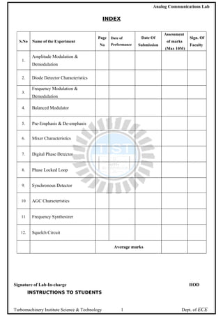
  • 1. Analog Communications Lab INDEX S.No 1. 2. 3. Name of the Experiment Page No Date of Performance Date Of Submission Assessment of marks (Max 10M) Sign. Of Faculty Amplitude Modulation & Demodulation Diode Detector Characteristics Frequency Modulation & Demodulation 4. Balanced Modulator 5. Pre-Emphasis & De-emphasis 6. Mixer Characteristics 7. Digital Phase Detector 8. Phase Locked Loop 9. Synchronous Detector 10 AGC Characteristics 11 Frequency Synthesizer 12. Squelch Circuit Average marks Signature of Lab-In-charge HOD INSTRUCTIONS TO STUDENTS Turbomachinery Institute Science & Technology 1 Dept. of ECE
  • 2. Analog Communications Lab Students shall read the points given below for understanding the theoretical concepts and Practical applications. 1. Listen carefully to the lecture given by teacher about importance of subject, curriculum philosophy, Learning structure, skills to be developed, information about equipment, instruments, procedure, method of continuous assessment, tentative plan of work in Laboratory and total amount of work to be done in a semester. 2. Students shall undergo study visit of the laboratory for types of equipment, instruments and material to be used, before performing experiments. 3. Read the write up of each experiment to be performed, a day in advance. 4. Organize the work in the group and make a record of all observations. 5. Understand the purpose of experiment and its practical implications. 6. Student should not hesitate to ask any difficulty faced during conduct of practical / exercise. 7. Student shall develop maintenance skills as expected by the industries. 8. Student should develop the habit of pocket discussion / group discussion related to the experiments/ exercises so that exchanges of knowledge / skills could take place. 9. Student should develop habit to submit the practical, exercise continuously and progressively on the scheduled dates and should get the assessment done. 10. Student shall attempt to develop related hands - on - skills and gain confidence. 11. Student shall focus on development of skills rather than theoretical or codified knowledge. 12. Student shall visit the nearby workshops, workstation, industries, laboratories, technical exhibitions trade fair etc. even not included in the Lab Manual. In short, students should have exposure to the area of work right in the student hood. 13. Student shall develop the habit of evolving more ideas, innovations, skills etc. those included in the scope of the manual. 14. Student shall refer to technical magazines, proceedings of the Seminars, refer websites related to the scope of the subjects and update their knowledge and skills. Turbomachinery Institute Science & Technology 2 Dept. of ECE
  • 3. Analog Communications Lab 15. The student shall study all the questions given in the laboratory manual and practice to write the answers to these questions. Exp No: 1 Date: AMPLITUDE MODULATION & DEMODULATION AIM: To study the function of Amplitude Modulation & Demodulation (under modulation, perfect modulation & over modulation) and also to calculate the modulation index. APPARATUS REQUIRED: S. No. 1 Component Transistor 2 Resistors 3 Capacitors 4 5 6 7 8 9 Diode Functions Generator Regulated Power Supply Bread Board Cathode Ray Oscilloscope Connecting Wires Specification BC107 100KΩ 4.7KΩ 270 Ω 33 Ω 4.7µF 0.001µF 0A79 1Mhz (0-30)V 0-20MHz Single Strand Quantity 2 2 2 1 1 2 1 1 2 1 1 1 As Required THEORY: Modulator section illustrates the circuit of modulating amplifier employing a transistor as an active device in CE mode. R1 & R2 establish a quiescent forward bias for the transistor. The modulating signal fed at the emitter section causes the bias to increase or decrease in accordance with the modulating signal. C3 is bypass capacitor for carrier. Thus the carrier signal applied at the base gets amplified more when the amplitude of the modulating signal is at its maximum and less when the amplitude of the modulating signal is small. C 2 couples the modulated signal to output of the modulator. Demodulation involves two operations. i) Rectification of the modulated signal and ii) Elimination of RF components of the rectified signal. Turbomachinery Institute Science & Technology 3 Dept. of ECE
  • 4. Analog Communications Lab The diode in the circuit diagram of demodulator does half wave rectification. The rectified signal is applied to a low pass filter to extract the modulating signal. CIRCUIT DIAGRAM: VCC = 12V R1 R3 C2 Output C1 B RF Input C L1 100µH BC 107 R2 E R4 C3 AF Input Demodulator: D1 AM Input AF Output OA 79 1KΩ 1nF EXPECTED WAVEFORMS:- Turbomachinery Institute Science & Technology 4 Dept. of ECE
  • 5. Analog Communications Lab PROCEDURE: 1. Made the connections according to Circuit Diagram. 2. Measure and note down the frequency & amplitude (p-p) of the fixed carrier signal. 3. Measure and note down the frequency & amplitude (p-p) of the fixed message signal. 4. Apply fixed frequency carrier signal to RF input terminals. 5. Apply modulating signal to AF input terminals. 6. Note down and trace the modulated signal envelope on the CRO screen. 7. Find the modulation index by measuring Vmax and Vmin from the modulated (detected/ traced) envelope. m=(Vmax –Vmin)/(Vmax+Vmin) 8. Repeat the steps 4,5 & 6 by changing the amplitude of the modulating signal so as to observe over modulation, under modulating and perfect modulation. 9. For demodulation, apply the amplitude modulated signal as an input to the demodulator and verify the demodulated output with respect to the applied modulating signal PRECAUTIONS: RESULT: Turbomachinery Institute Science & Technology 5 Dept. of ECE
  • 6. Analog Communications Lab Turbomachinery Institute Science & Technology 6 Dept. of ECE
  • 7. Analog Communications Lab QUESTIONS Tm 1. AM is Defined as ____________ 2. Draw its spectrum___________ 3. Draw the phase representation of an amplitude modulated wave___ 4. Modulation index is defined as_____ 5. The different degrees of modulation _______ 6. What are the limitations of square law modulator 7. Compare linear and nonlinear modulators 8. Compare base modulation and emitter modulation 9. AM Demodulator is ___________ 10. Detection process _________ 11. The different types of distortions that occur in an envelop detector are__________ 12. Elimination of distortions in Envelope Detector __________________ technique we use. Turbomachinery Institute Science & Technology 7 Dept. of ECE
  • 8. Analog Communications Lab Turbomachinery Institute Science & Technology 8 Dept. of ECE
  • 9. Analog Communications Lab Turbomachinery Institute Science & Technology 9 Dept. of ECE
  • 10. Analog Communications Lab Turbomachinery Institute Science & Technology ECE 10 Dept. of
  • 11. Analog Communications Lab Turbomachinery Institute Science & Technology ECE 11 Dept. of
  • 12. Analog Communications Lab Exp No: 2 Date: DIODE DETECTOR CHARACTERISTICS AIM: To perform demodulation of an amplitude modulated signal using (i) Simple diode detector and (ii) Practical diode detector APPARATUS REQUIRED: S. No. 1 Component Transistor 2 Resistors 3 Capacitors 4 5 6 7 8 9 10 Diode Functions Generator Regulated Power Supply Bread Board Cathode Ray Oscilloscope Potentiometer Connecting Wires THEORY: Specification BC107 100KΩ 4.7KΩ 270 Ω 33 Ω 4.7µF 0.001µF Variable 0A79 1Mhz (0-30)V 0-20MHz 100K Ω Single Strand Quantity 2 2 2 1 1 2 1 2 1 2 1 1 1 1 As Required Demodulation involves two operations: (i) Rectification of the modulated wave and (ii) Elimination of RF components of the rectified modulated wave Simple Diode Detector The diode is the most common device used in AM demodulator. Signal (AM modulated signal) is applied to anode and output is taken from cathode. Diode operates as half wave rectifier and passes only positive half cycle of the modulated wav e. Further signal is applied to a parallel combination of resistor (Rd) and capacitor (Cd) which acts as a low pass filter. This LPF allows only low frequency signal to output and it by passes RF component to the ground. This simple diode detector has the disadvantage that the output voltage, in addition to being proportional to the modulating signal, also has a dc component, which represents the average envelope amplitude (i.e. carrier signal) and a small RF ripple. However these unwanted components are removed in a practical detector leaving only AF signal. CIRCUIT DIAGRAM: Turbomachinery Institute Science & Technology ECE 12 Dept. of
  • 13. Analog Communications Lab EXPECTED WAVEFORMS:- AM Modulated signal Practical Diode Detector: Turbomachinery Institute Science & Technology ECE 13 Dept. of
  • 14. Analog Communications Lab In practical diode detector the cathode terminal of the diode is connected to one end of the secondary of IF transformer. The other end is grounded. Secondary is tuned with the capacitor C1. The capacitors C2 and C3 are used for RF filtering. The modulated signal is applied at the input of IF transformer. The voltage applied is negative and hence the cathode of the diode passes is connected to the IF transformer. So the diode passes both the positive and negative half cycles. The RF filtering is done by C2 and C3. The output is taken at the volume control. PROCEDURE:1. Connect the circuit as per the circuit diagram and switch on the power supply. ( Measure the power supply voltage, +12V and -12V) 2. Observe outputs of RF and AF signal generator using CRO, note that RF voltage is approximately 300mv p-p of 1MHz frequency and AF voltage is 10V p-p 2KHz frequency. 3. Now connect the modulator output to the simple diode detector input. 4. Observe the AF signal at the output to the simple diode detector at approximately 50% modulation using CRO. 5. Compare it with the original AF and observe that the detected signal is same as the AF signal applied. Thus no information is lost in the process of modulation. (Note: Only wave shape and frequency will be same, amplitude will be attenuated and phase may change) 6. To observe AM wave at different frequencies, connect AF signal from external signal generator to the input of modulator and observe demodulated wave at different frequencies. 7. Repeat the experiment using practical diode detector circuit. PRECAUTIONS: RESULT: Turbomachinery Institute Science & Technology ECE 14 Dept. of
  • 15. Analog Communications Lab AF output QUESTIONS Tm Turbomachinery Institute Science & Technology ECE 15 Dept. of
  • 16. Analog Communications Lab 1. Selectivity of receiver is defined as _____________ 2. Sensitivity of a receiver is defined as ____________ 2. The purpose of diode in diode detector circuit is __________ 3. The disadvantages of simple diode detector circuit are _______ 4. The factors influencing the choice of intermediate frequency in receivers _____ 5. The advantages of practical diode detector are________ Turbomachinery Institute Science & Technology ECE 16 Dept. of
  • 17. Analog Communications Lab Turbomachinery Institute Science & Technology ECE 17 Dept. of
  • 18. Analog Communications Lab Turbomachinery Institute Science & Technology ECE 18 Dept. of
  • 19. Analog Communications Lab Turbomachinery Institute Science & Technology ECE 19 Dept. of
  • 20. Analog Communications Lab Exp No: 3 Date: FREQUENCY MODULATION AND DEMODULATION AIM: To study the functioning of frequency modulation & demodulation and to calculate the modulation index. APPARATUS REQUIRED S. No. 1 Component ICs 2 Resistors 3 Capacitors 4 5 6 7 8 Specification XR 2206, LM 565 100KΩ, 4.7KΩ 10KΩ 220Ω 47KΩ 0.01µF,0.001µF 0. 1µF, 470pF, 0.01pF 1µF,10µF 1Mhz (0-12)V Functions Generator Regulated Power Supply Bread Board Cathode Ray Oscilloscope Connecting Wires 0-20MHz Single Strand Quantity 1 Each 2 Each 1 1 1 2 1 1 2 1 1 1 As Required THEORY: 1. AF Generator: This is an op-amp placed wein bridge oscillator. A FET input quad Op-Amp (ICTL084) is used here to generate low frequency signals of 500 Hz and 5KHz to use as modulating signal. In this experiment, a switch is provided to change the frequency. Required amplification is provided to avoid loading effect. 2. Regulated power supply: This consists of bridge rectifier, capacitor filters and three terminal regulators to provide required dc voltages in the circuit i.e. +15 V, -15 V, +5V . 3. Modulator: This has been developed using XR-2206 integrated circuit. The IC XR-2206 is a monolithic Function generator; the output waveforms can be both amplitude and frequency modulated by an external voltage. Frequency of operation can be selected externally over a range of 0.01 MHz. The circuit is ideally suited for communications, instrumentations and function generator applications requiring CIRCUIT DIAGRAM: Frequency Modulation Circuit Diagram: +12v Turbomachinery Institute Science & Technology ECE 4.7KΩ 20 Dept. of
  • 21. Analog Communications Lab 4 100KΩ 7 47KΩ 3 AF I/F 10µF/63v FM O/P 2 10KΩ 4.7 KΩ 0.1µF XR 2206 14 220Ω 5 0.01µF 6 13 1 10 1µF/63v Frequency Demodulation Circuit Diagram: + 5v 10KΩ 10 10KPF 2 0.1µF AF Input 8 680Ω 1KPF LM 565 7 AF Output 4 3 5 1 9 680Ω 470PF – 5V sinusoidal tone, AM, FM or FSK generation. In this experiment, IC XC-2206 is connected to generate sine wave, which is used as a carrier signal. The amplitude of carrier signal is 5vPP of 100 KHz frequencies. 4. Demodulator: Turbomachinery Institute Science & Technology ECE 21 Dept. of
  • 22. Analog Communications Lab This had been developed using LM4565 integrated circuit. The IC LM565 is a generalpurpose phase locked loop containing a stable, highly linear voltage controlled oscillator for low distortion FM demodulation. The VCO free running frequency f0 is adjusted to the center frequency of input frequency modulated signal i.e. carrier frequency which is of 100 KHz. When FM signal is connected to the demodulator input, the deviation in the input signal (FM signal) frequency which creates a DC error voltage at output of the phase comparator which is proportional to the change of frequency δf. This error voltage pulls the VCO to the new point. This error voltage will be the demodulated version of the frequency modulated input signal. PROCEDURE: 1. Connect the circuit as per the given circuit diagram. 2. Switch on the power supply. 3. Measure the frequency of the carrier signal at the FM output terminal with input terminals open and plot the same on graph. 4. Apply the modulating signal of 500HZ with 1Vp-p. 5. Trace the modulated wave on the C.R.O & plot the same on graph. 6. Find the modulation index by measuring minimum and maximum frequency deviations from the carrier frequency using the CRO. Mr = S maximum Frequency deviation = f modulating signal frequency 7. Repeat the steps 5& 6 by changing the amplitude and /or frequency of the modulating Signal. 8. For demodulation apply the modulated signal as an input to demodulator circuit and compare the demodulated signal with the input modulating signal & also draw the same on the graph. NOTE: Note down all the input and output wave forms of the signals applied and obtained respectively. PRECAUTIONS: RESULT: Turbomachinery Institute Science & Technology ECE 22 Dept. of
  • 23. Analog Communications Lab EXPECTED WAVEFORMS: Turbomachinery Institute Science & Technology ECE 23 Dept. of
  • 24. Analog Communications Lab Turbomachinery Institute Science & Technology ECE 24 Dept. of
  • 25. Analog Communications Lab QUESTIONS 1. Frequency modulation is defined as ____ 2. The advantages of indirect method of FM generation are __ 3. Modulation index and frequency deviation of FM is ____ 4. The advantages of FM are ______ 5. Narrow band FM is _____ 6. Compare narrow band FM and wide band FM? 7. Differentiate FM and AM _____ 8. FM wave can be converted into PM wave _____ 9, State the principle of reactance tube modulator _____ 10. The bandwidth of FM system is ___ 11. The function of FM discriminator is_________ 12. Ratio detector differ from foster-seely discriminator _____ 13. Linear detector is ________ 14. The drawbacks of slope detector are ___________ Turbomachinery Institute Science & Technology ECE 25 Dept. of
  • 26. Analog Communications Lab Turbomachinery Institute Science & Technology ECE 26 Dept. of
  • 27. Analog Communications Lab Turbomachinery Institute Science & Technology ECE 27 Dept. of
  • 28. Analog Communications Lab E Turbomachinery Institute Science & Technology ECE 28 Dept. of
  • 29. Analog Communications Lab xp No: 4 Date: BALANCED MODULATOR AIM: To study the following of the Balanced Modulator as a 1. Frequency Doubler 2. DSB-SC Generator. APPARATUS REQUUIRED: S. No. 1 Component Modulator IC 2 Resistors 3 Capacitors 5 6 7 8 9 Functions Generator Regulated Power Supply Bread Board Cathode Ray Oscilloscope Connecting Wires Specification MC1496 10KΩ 4.7KΩ 270 Ω 33 Ω 0.1µF 0.001µF 1Mhz (0-30)V 0-20MHz Single Strand Quantity 2 3 2 1 1 4 1 2 1 1 1 As Required THEORY: 1. RF Generator: Colpitts oscillator using FET is used here to generate RF signal of approximately 100 KHz Frequency to use as carrier signal in this experiment. Adjustments for Amplitude and Frequency are provided in panel for ease of operation. 2. AF Generator: Low Frequency signal of approximately 5KHz is generated using OP-AMP based Wein- Bridge oscillator. IC TL 084 is used as an active component; TL 084 is FET input general purpose quad OP-AMP integrated circuit. One of the OP-AMP has been used as amplifier to improve signal level. Facility is provided to change output voltage. 3. Regulated Power Supply: This consists of bridge rectifier, capacitor filters and three terminal regulators to provide required DC voltage in the circuit i.e. +12v, -8v @ 150 MA each. CIRCUIT DIAGRAM: Turbomachinery Institute Science & Technology ECE 29 Dept. of
  • 30. Analog Communications Lab 4. Modulator: Turbomachinery Institute Science & Technology ECE 30 Dept. of
  • 31. Analog Communications Lab The IC MC 1496 is used as Modulator in this experiment. MC 1496 is a monolithic integrated circuit balanced modulator/Demodulator, is versatile and can be used up to 200 Mhz. Multiplier: A balanced modulator is essentially a multiplier. The output of the MC 1496 balanced modulator is proportional to the product of the two input signals. If you apply the same sinusoidal signal to both inputs of a ballooned modulator, the output will be the square of the input signal AM-DSB/SC: If you use two sinusoidal signals with deferent frequencies at the two inputs of a balanced modulator (multiplier) you can produce AMDSB/ SC modulation. This is generally accomplished using a high- frequency “carrier” sinusoid and a lower frequency “modulation” waveform (such as an audio signal from microphone). The figure 1.1 is a plot of a DSB-SC waveform, this figure is the graph of a 100KHz and a 5 KHz sinusoid multiplied together. Figure 1.2 shows the circuit that you will use for this experiment using MC 1496 balanced modulator/demodulator. Note: In frequency doubling If the input time period is “T” after frequency doubling the time period should be halfed.i.e,”T/2”. PROCEDURE:I-Frequency Doubler 1. Connect the circuit as per the given circuit diagram. 2. Switch on the power to the trainer kit. 3. Apply a 5 KHz signal to both RF and AF inputs of 0.1VP-P. 4. Measure the output signal frequency and amplitude by connecting the output to CRO. 5. Repeat the steps 3 and 4 by changing the applied input signal frequency to 100KHZ and 500KHz. And note down the output signals. NOTE: - Amplitude decreases with increase in the applied input frequency. II-Generation of DSB-SC 1. For the same circuit apply the modulating signal(AF) frequency in between 1Khz to 5Khz having 0.4 VP-P and a carrier signal(RF) of 100KHz having a 0.1 VP-P . 2. Adjust the RF carrier null potentiometer to observe a DSB-SC waveform at the output terminal on CRO and plot the same. Repeat the above process by varying the amplitude and frequency of AF but RF maintained constant. NOTE:- Note down all the waveforms for the applied inputs and their respective outputs. PRECAUTIONS: EXPECTED WAVEFORMS: Turbomachinery Institute Science & Technology ECE 31 Dept. of
  • 32. Analog Communications Lab Turbomachinery Institute Science & Technology ECE 32 Dept. of
  • 33. Analog Communications Lab Turbomachinery Institute Science & Technology ECE 33 Dept. of
  • 34. Analog Communications Lab RESULT: QUESTIONS 1. The two ways of generating DSB_SC are ________ 2. The applications of balanced modulator are ________ 3. The advantages of suppressing the carrier ________ 4. The advantages of balanced modulator __________ 5. The advantages of Ring modulator __________ 6. The expression for the output voltage of a balanced modulator is _________ Turbomachinery Institute Science & Technology ECE 34 Dept. of
  • 35. Analog Communications Lab Turbomachinery Institute Science & Technology ECE 35 Dept. of
  • 36. Analog Communications Lab Turbomachinery Institute Science & Technology ECE 36 Dept. of
  • 37. Analog Communications Lab Turbomachinery Institute Science & Technology ECE 37 Dept. of
  • 38. Analog Communications Lab Exp No: 5 Date: PRE-EMPHASIS & DE-EMPHASIS AIM: To study the functioning of Pre-Emphasis and De-Emphasis circuits. APPARATUS REQUIRED: S. No. 1 Component Resistors 2 Capacitors 3 4 5 6 7 Functions Generator Regulated Power Supply Bread Board Cathode Ray Oscilloscope Connecting Wires Specification 1KΩ 0.1µF 0.001µF 1Mhz (0-30)V 0-20MHz Single Strand Quantity 2 2 1 2 1 1 1 As Required THEORY: Frequency modulation is much immune to noise than amplitude modulation and significantly more immune than phase modulation. A single noise frequency will affect the output of the receiver only if it falls with in its pass band. The noise has a greater effect on the higher modulating frequencies than on lower ones. Thus, if the higher frequencies were artificially boosted at the transmitter and correspondingly cut at the receiver, improvement in noise immunity could be expected. This booting of the higher frequencies, in accordance with a pre-arranged curve, is termed pre-emphasis, and the compensation at the receiver is called deemphasis. If the two modulating signals have the same initial amplitude, and one of them is pre-emphasized to (say) twice this amplitude, whereas the other is unaffected (being at a much lower frequency) then the receiver will naturally have to de-emphasize the first signal by a factor of 2, to ensure that both signals have the same amplitude in the output of the receiver. Before demodulation, i.e. while susceptible to noise interference the emphasized signal had twice the deviation it would have had without pre-emphasis, and was thus more immune to noise. Alternatively, it is seen that when this signal is de-emphasized any noise sideband voltages are de-emphasized with it, and therefore have a correspondingly lower amplitude than they would have had without emphasis again their effect on the output is reduced. The amount of preemphasis in U.S FM broadcasting, and in the sound transmissions accompanying television, has been standardized at 75 microseconds, whereas a number of other services, notably CCIR and Australian TV sound transmission, use 50 micro second. CIRCUIT DIAGRAM: Turbomachinery Institute Science & Technology ECE 38 Dept. of
  • 39. Analog Communications Lab Turbomachinery Institute Science & Technology ECE 39 Dept. of
  • 40. Analog Communications Lab The usage of microseconds for defining emphasis is standard. 75 microseconds de-emphasis corresponds to a frequency response curve that is 3 db down at the frequency whose time constant is RC is 75 microseconds. This frequency is given by f=1/2ÐRC and it is therefore 2120 Hz; with 50-microseconds deemphasis it would have been 3180 Hz. Figure I shows pre emphasis and de-emphasis curves for a 7 microseconds emphasis, as used in the united states. If emphasis is applied to amplitude modulation, some improvement will also result, but it is not as great as in FM because the highest modulating frequencies in AM are no more affected by noise than any others. Apart from that, it would be difficult to introduce pre-emphasis and de-emphasis in existing AM services since extensive modifications would be needed, particularly in view of the huge numbers is receivers in use. PROCEDURE: I-PRE-EMPHASIS 1. Connect the circuit as per the circuit diagram 2. Apply a sine wave to the input terminals of 2 VP-P (Vi) 3. By varying the input frequency with fixed amplitude, note down the output amplitude (Vo) with respect to the input frequency. 4. Calculate the gain using the formula Gain = 20 log (VO/ VI) db Where VO = output voltage in volts. VI = Input voltage in volts. And plot the frequency response. II-DE-EMPHASIS 1. Connect the circuit as per circuit diagram. Repeat steps 2, 3 & 4 of Pre-Emphasis to de-emphasis also. PRECAUTIONS: RESULT: Turbomachinery Institute Science & Technology ECE 40 Dept. of
  • 41. Analog Communications Lab Turbomachinery Institute Science & Technology ECE 41 Dept. of
  • 42. Analog Communications Lab QUESTIONS 1. The need for pre-emphasis __________ 2. The operation of pre-emphasis circuit __________ 3. Pre-emphasis operation is similar to high pass filter explain how_______ 4. De-emphasis operation is similar to low pass filter justify _______ 5. De-emphasis is _______ 6. Draw the frequency response of a pre-emphasis circuit_______ 7. Draw the frequency response of a de-emphasis circuit ______ 8. Give the formula for the cutoff frequency of the pre-emphasis circuit ______ 9. The significance of the 3db down frequency is ______ Turbomachinery Institute Science & Technology ECE 42 Dept. of
  • 43. Analog Communications Lab Turbomachinery Institute Science & Technology ECE 43 Dept. of
  • 44. Analog Communications Lab Turbomachinery Institute Science & Technology ECE 44 Dept. of
  • 45. Analog Communications Lab Turbomachinery Institute Science & Technology ECE 45 Dept. of
  • 46. Analog Communications Lab Turbomachinery Institute Science & Technology ECE 46 Dept. of
  • 47. Analog Communications Lab Exp No: 6 Date: CHARACTERISTICS OF MIXER AIM: To study the functioning of a frequency mixer. APPARATUS REQUIRED: S. No. Component 1 Resistors 2 Capacitors 3 4 5 6 7 8 Transistor Functions Generator Regulated Power Supply Bread Board Cathode Ray Oscilloscope Connecting Wires Specification 4.7KΩ, 22KΩ,3.3KΩ 27KΩ, 6.2KΩ 10KΩ 0.1µF, 50pF 0.1µF 100pF BC 547 1Mhz (0-30)V 0-20MHz Single Strand Quantity 1 3 3 2 2 4 1 2 1 1 1 As Required THEORY: The fundamental principle of modulation involves the mixing or multiplying of a low frequency signal with a higher frequency signal such as an AM or FM carrier. This enables the information contained in the low frequency signal to be transmitted through space as high frequency electromagnetic waves. Commercial radios use as intermediate frequency (455 khz for commercial AM). These if carrier contain all the information available to the receiver but in order to obtain this information mixing must take place to obtain the lower frequency signals ‘riding’ onto IF or RF frequency. This principle is also used in mixing low frequency signals up to IF or RF frequencies. The purpose of this experiment is to observe the effect of mixing two frequencies using a nonlinear single transistor mixer and to demonstrate the use of a band stop and a 2-pole low pass filter in a practical application. BLOCK DIAGRAM DESCRIPTION: 1. RF Generator 1: Colpitts oscillator using FET is used here to generate RF signal of approximately 500 KHz to use as local oscillator in this experiment. Adjustments for amplitude and Frequency are provided on panel for ease of operation. Turbomachinery Institute Science & Technology ECE 47 Dept. of
  • 48. Analog Communications Lab CIRCUIT DIAGRAM: 12V 50pF 50pF 3.3KΩ 22KΩ 4.7KΩ 27KΩ 6.2KΩ 6.2KΩ 27KΩ Output C 0.1µF B BC 547 100pF 100pF 100pF VX E 0.1µF VY 10KΩ 10KΩ 10KΩ EXPECTED WAVEFORMS: 2. RF Generator 2: Turbomachinery Institute Science & Technology ECE 48 Dept. of
  • 49. Analog Communications Lab Colpitts oscillator using FET is used here to generate RF signal of approximately 520 KHz to use as IF Signal in this experiment. Adjustment for Frequency is provided on panel to get exact frequency. 3. Regulated Power Supply: This consists of bridge rectifier, capacitor filters and three terminal regulators to provide required do voltage in the circuit i.e., +12v @150 mA. 4. Mixer: Mixing is the nonlinear combination of two signals to produce sum and difference frequencies and harmonics of the signals. It is primarily used for modulation of demodulation of a signal. Modulation is the translation of the signal information to a higher frequency signal, and demodulation is the translation of signal / information carried by high frequency signal down to a lower frequency. The principle involved in this experiment is the use of the nonlinear portion of a transistor characteristic to mix (combine) two signals. Below figure shows the circuit you will use in this experiment. The Vy input the local oscillator and is made large so that the signal is cut off at the Collector. This forces the transistor to operate in a very nonlinear region. Now that the transistor is operating in a nonlinear regional during part of its cycle the input signal representing an input from the IF of a radio, is introduced at a low level (millvolts). The result is an output at the collector at the transistor that contains all the frequencies (sum, difference and high frequence harmonics) An example if Vyis 500 Khz and Vx is 520 Khsz the output frequencies at the collector will be do, dc, 20 Khz, 20 Khz, I Mhz, 1.092 MHz and other harmonics of the sum frequencies, the difference frequencies, and the original frequencies. In a radio you are interested only in the audio output: therefore you need to eliminate all higher frequencies. In this circuit you are interested only in the 20 Khz signal (which is above the usual audio range but provides a good signal on many spectrum analyzers), so you must design a filter to eliminate all the higher frequency signals. The 500 Khz component is the largest in the output because of the very large signal generated by the local oscillator (Vy). Thus a special notch filter will be used to attenuate this large singnal and a low pass filter will be used to attenuate other harmonics. Turbomachinery Institute Science & Technology ECE 49 Dept. of
  • 50. Analog Communications Lab TABULAR COLOUMN: S.NO Inputs Vx sin (2∏fxt) Turbomachinery Institute Science & Technology ECE Filter Output Vy sin (2∏fyt) 50 Vo sin (2∏fot) Dept. of
  • 51. Analog Communications Lab PROCEDURE: 1. Connect the circuit as per the circuit diagram. 2. Observe the output signal of RF generator 1 and 2 using CRO and note that output voltage of RF generator 1 is approximately 3VPP (frequency between 400 to 550 KHz) and RF generator 2 is approximately 0.6VPP (frequency between 550KHz). 3. Set RF generator 1 output at 500KHz with the help of IFT and connect it to the V Y input (which represents local oscillator) of the mixer circuit. 4. Observe the signal at output using CRO. Vary the amplitude of the RF generator 1 using potentiometer until the signal at output is noticeably nonlinear (note that the signal is clipped). The clipping is necessary to introduce nonlinearities, which is how the sum and difference frequencies and other harmonics are produced. 5. Set RF generator 2 output at 520KHz with the help of IFT and connect it to the V X input (which represents IF signal) of the mixer circuit and observe the signal at mixer output using CRO. 6. Connect output of mixer to filter input and observe output signal. Note that the signal is approximately 0.7VPP of 20KHz frequency. 7. Change VX and VY signal frequencies and observe output signal. PRECAUTIONS: RESULT: QUESTIONS: 1. The need for a frequency mixer is _________ 2. Heterodyning is 3. ___________filter is used at the o/p of transistor circuit in a frequency mixer? 4. The frequency components that appear at the collector of the transistor in the mixer circuit are __ 5. The transistor operated in the nonlinear region in a frequency mixer because ________________ Turbomachinery Institute Science & Technology ECE 51 Dept. of
  • 52. Analog Communications Lab Turbomachinery Institute Science & Technology ECE 52 Dept. of
  • 53. Analog Communications Lab Turbomachinery Institute Science & Technology ECE 53 Dept. of
  • 54. Analog Communications Lab Turbomachinery Institute Science & Technology ECE 54 Dept. of