1. Pt redistribution during NiSi formation
J. Demeulemeester, D. Smeets, and A. Vantomme
Instituut voor Kern- en Stralingsfysica and INPAC,
KULeuven, B-3001 Leuven, Belgium
C. Detavernier and C. Van Bockstael
Vakgroep Vaste-stofwetenschappen, Universiteit Gent, B-9000 Gent, Belgium
C. M. Comrie
Department of Physics, University of Cape Town, Rondebosch 7700, South Africa
N. P. Barrades
Instituto Tecnol´gico e Nuclear, Estrada Nacional 10, Apartado 21, 2686-953,
o
Sacav´m, Portugal and Centro de F´
e isica Nuclear da Universidade de Lisboa,
Av. Prof. Gama Pinto 2, 1699, Lisboa Codex, Portugal
A. Vieira
Instituto Superior de Engenhariado do Porto, Portugal
(Dated: September 29, 2008)
Abstract
We report on a real-time Rutherford backscattering spectrometry (RBS) study of the erratic
redistribution of Pt during Ni silicide formation in a solid phase reaction. The inhomogeneous
Pt redistribution in Ni(Pt)Si films is a consequence of the low solubility of Pt in Ni2 Si compared
to NiSi and the measured limited mobility of Pt in NiSi. Pt further acts as a diffusion barrier
and resides in the Ni2 Si grain boundaries, significantly slowing down the Ni2 Si and NiSi growth
kinetics. Moreover, the observed incorporation of a large amount of Pt in the NiSi seeds indicates
that Pt plays a major role in the development of the Ni(Pt)Si texture.
1
2. Ni(Pt)Si thin film alloys are currently used as contact layers in CMOS technology. Adding
Pt to the compound results in an increased thermal stability of the monosilicide thin film1 .
The exact role of Pt in this stabilization effect is not completely understood. Pt has a
distinct influence on the NiSi texture, causing stabilization in terms of interface energy2 . It
is believed that the NiSi lattice expansion caused by the incorporation of Pt lies at the origin
of the dependence between the texture and the initial Pt concentration. This interpretation
however critically depends on the amount of Pt present at the NiSi/Si interface in the initial
stage of Ni(Pt)Si formation, as it are those seeds that determine the overall final texture.
Cojocaru-Mir´din et al.3 have shown that Pt does not remain homogeneously distributed
e
throughout the thermal treatment, but gets extruded in a snowplow process. As such, Pt
influences the growth kinetics by acting as a diffusion barrier. Furthermore, Pt incorporation
into the NiSi matrix is expected to have a distinct influence on stress during formation, which
plays a major role in determining the mechanical, morphological and electrical properties
of the Ni(Pt)Si thin film. Hence, to understand the influence of the Pt addition on texture
development, the growth kinetics as well as the stress behavior, detailed information on the
Pt distribution during annealing is crucial. Such information is readily accessible with real-
time Rutherford backscattering spectrometry (RBS)4 measurements as will be elucidated
below.
A set of 75 nm thick homogeneous Ni(Pt) alloys with Pt concentrations of 1, 3, 7 and
10 at.%, were sputtered on RCA cleaned Si(100) substrates. All samples were annealed in
high-vacuum (∼10−7 Torr) at a heating rate of 2 ◦ C/min while simultaneously conducting
RBS with a 2 MeV He beam (backscattering-angle=165 ◦ ). The ramped anneals were
continued until no further redistribution was observed for at least 20 minutes. A prolonged
annealing (ramped at 2 ◦ C/min to 600 ◦ C for 30 min) was applied to the sample with 7 at.%
Pt to investigate the thermal stability of the Pt distribution in the NiSi phase. Artificial
neural networks (ANNs)5 were used for the quantitative analysis of all acquired RBS spectra.
This analysis yields the thickness of the individual phases growing during the annealing, as
well as detailed information on the relative atomic concentrations throughout the film and
throughout the annealing process.
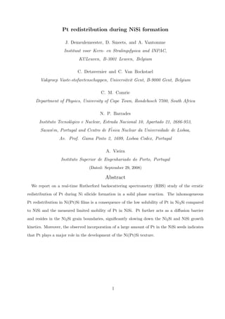
Figure 1(a) shows two RBS spectra captured during the annealing of a film with 3 at.%Pt.
The squares and dots represent the RBS spectra acquired at room temperature and 450 ◦ C
respectively. Three regions, corresponding to the three elements in the specimen, can be
2
3. distinguished in these spectra. Channels (x-axis) 150-280 cover the Si signal, channels 310-
390 the Ni signal and channels 400-465 cover the Pt signal. From the energy loss, a depth
scale, as shown in Fig. 1(a), can be associated with each element, with the highest energy
(channel) corresponding to elements at the surface. The relative height of the signals, i.e.
the backscattering yield (y-axis), is a measure for the elemental concentration in the film.
Hence, RBS spectra provide quantitative, depth sensitive information on the composition
of the analyzed films. The higher Ni signal for the as deposited specimen in Fig. 1(a)
shows that the relative Ni content in the surface layer is higher for the as deposited film
compared to the annealed film. For comparison the theoretical heights for a pure Ni film,
a pure Ni2 Si film, and a pure NiSi film are indicated in the picture, which shows that a
NiSi film has formed after annealing. The larger width of the Ni signal after annealing
on the other hand, shows that the Ni(Pt)Si film is thicker than the initial Ni(Pt) film.
For more details on RBS and the interpretation of RBS spectra, the reader is directed
to the literature6 . From the RBS spectra in Fig. 1 (a) it can be deduced that despite the
homogeneous Pt distribution in the as-deposited metal alloy, an absolutely not homogeneous
Pt distribution is established in the final Ni(Pt)Si film. Three Pt concentration regions can
be distinguished and are shown in the inset of Fig. 1 (a). In channels 400-420 a region with
a very low Pt concentration (ANN-analysis yields Pt/Ni∼0.3 at.%, thickness ≈ 98nm) is
found near the silicide/Si interface, followed by a Ni(Pt)Si layer in the middle of the film
that is very rich in Pt (Pt/Ni∼6 at.%, t ≈ 77nm) (channels 420-435) and finally a silicide
with a moderate Pt concentration (Pt/Ni∼1 at.%, t ≈ 96nm) is found at the surface of
the film. However, for a thorough understanding of the role of Pt and its redistribution
in texture and stress development, thermal stability, growth kinetics etc., an investigation
of the sample at the end of the annealing sequence only, as shown in Fig. 1 (a) is largely
insufficient. Detailed, depth sensitive information on the film composition throughout the
growth process, as provided by real-time RBS, is therefore crucial to grasp the full formation
process. Moreover, the especially high sensitivity of RBS to heavy elements enables accurate
investigation of specimens with a low Pt concentration, making real-time RBS the ideal
technique to study the redistribution of Pt during Ni(Pt)-silicide formation.
Real-time RBS data are conveniently plotted in a contour plot as in Fig. 2, which shows
the data for the specimens containing 1, 3 and 10 at.% Pt. Every horizontal line in such
a contour plot corresponds to an RBS spectrum as shown in Fig. 1. The backscattering
3
4. yield is now represented by a color scale, with red indicating a high yield and blue a low
yield. The contour plot is constructed from the consecutively acquired RBS spectra during
annealing, the y-axis therefore represents the annealing temperature. For example, the
horizontal line at 375 ◦ C in Fig. 2(b) corresponds to the spectrum in Fig. 1 (b). The Si, Ni
and Pt regions can be distinguished in the contour plots and depth scales are added in Fig.
2 for interpretation purposes.
A first glance at Fig. 2 shows that the Pt distribution during silicide formation is quite
erratic. Performing this study ex situ and with discrete temperature steps would thus yield a
large risk to miss important steps in the formation process, favoring the real-time approach.
Focussing on the sample with 3 at. % Pt (Fig. 2(b)) it is clear that little or no reaction takes
place below 250 ◦ C . Above that temperature, the gradual broadening of the Ni signal and
the shift of the Si signal towards higher channel numbers mark the formation of the Ni2 Si
phase that coincides with the first inhomogeneities in the Pt distribution. At this stage of
the reaction, the low solubility of Pt in Ni2 Si3 results in the expulsion of Pt, causing a Pt
enrichment of the Pt alloy. This enriched layer is gradually pushed towards the surface,
i.e. higher channel numbers, as more Ni2 Si forms underneath in a process that is referred to
as the snowplow effect3 . As the Ni diffuses trough the Pt rich layer to form the Ni2 Si phase,
a fraction of the Pt is incorporated into the Ni2 Si layer. For all initial Pt concentrations
we observe a homogeneous Pt content in the Ni2 Si , that scales with the Pt concentration
in the as deposited alloy, but is markedly lower than that. These observations suggest that
the Pt amount in the Ni2 Si layer does not correspond to the solubility limit of Pt into
Ni2 Si. As such, Pt is more likely to reside at the silicide grain boundaries, supporting the
findings of Imbert et al.7 . During Ni2 Si formation increasingly more Pt is incorporated in
the Pt enriched layer that acts as a diffusion barrier. This is reflected in the increased
temperature for the complete silicidation that corresponds to the point where the Si signal
reaches channel 280, i.e. Si reaches the sample surface or the metal completely penetrated
the substrate. This point is achieved at ± 350 ◦ C for 1 at.% Pt, ± 375 ◦ C for 3 at.% Pt and
± 400 ◦ C for 10 at.% Pt.
At approximately 350 ◦ C for the 3 at.% Pt specimen (Fig.2.(b)), a new Pt contour appears
at low channel numbers (channel 425), i.e. the interface with the substrate. Figure 1(b) shows
the RBS spectrum measured at this temperature. Detailed analysis of this spectrum shows
that the appearance of this Pt contour coincides with the initial stage of NiSi formation,
4
5. as can be deducted from the shoulder at lower channel numbers in the Ni signal (indicated
by an arrow in Fig. 2(b)). The Pt concentration in this NiSi seed layer is very high in
contrast to the Ni2 Si layer, and even exceeds the initial concentration in the metal alloy.
This seed layer later develops into the middle, Pt rich, NiSi layer as already identified in
the final NiSi film (Fig. 1(a)). The high Pt concentration in the NiSi seed layer can be
understood by realizing that Pt is highly soluble in NiSi compared to Ni2 Si . This presents
a driving force for the integration of Pt into the freshly formed NiSi seeds. Consequently,
the Pt concentration in the Ni2 Si layer decreases as the NiSi seed layer is forming. Pt thus
diffuses out of the Ni2 Si layer and is incorporated in the growing NiSi.
At slightly higher temperatures (∼390 ◦ C , Fig.2(b), 3 at.%Pt), the RBS signal of this Pt
rich NiSi layer starts to shift to higher channels, due to the formation of another NiSi layer
underneath, with a much lower Pt concentration. At the same time a third NiSi layer forms
on top of the Pt rich NiSi. Once the reaction is completed, the thin film is transformed
into a NiSi film with three distinct regions in Pt concentration as mentioned before, with
the Pt rich NiSi seed layer exactly in the center of the film (Fig. 1(a)). The origin of this
final configuration lies within the growth of NiSi at two interfaces. Above the Pt rich NiSi
layer, Ni2 Si dissociates into NiSi and Ni. The atomic Ni diffuses through the NiSi seed layer
and forms NiSi at the interface with the substrate. Pt outdiffusion from the Pt rich NiSi
layer and drag effects are limited, which results in the low Pt concentration in this layer.
The Pt concentration gradient in this layer however, shows that these effects are present.
For the NiSi layer that forms from the dissociation of Ni2 Si on top of the Pt rich layer, Pt
is available and directly incorporated in the forming monosilicide. The Pt concentration in
this layer is therefore equal to that in the Ni2 Si layer. We want to point out that the same
triple layered structure is obtained after reacting a 30 nm Ni(Pt) film, indicating that the
formation process is independent of the thin film thickness.
To investigate the thermodynamical stability of the Pt configuration after complete NiSi
formation, an extended annealing of the 7 at.% Pt specimen at 600 ◦ C for 30 min was
performed while continuing the real-time RBS measurement. Although this inhomogeneous
Pt distribution throughout the full NiSi film is thermodynamical relatively unstable, only
a marginal redistribution of the Pt could be observed. This proves that the Pt mobility in
NiSi is very low at temperatures as high as 600 ◦ C .
As illustrated, the addition of Pt has a major influence on the Ni silicide growth kinetics,
5
6. since the formation of a Pt rich diffusion barrier limits the supply of Ni at the Ni2 Si growth
interface. The presence of Pt at the Ni2 Si grain boundaries, where the majority of the mass
transport takes place further limits this supply, which is reflected in the delay of the complete
silicidation to higher temperatures for higher initial Pt concentrations. The slowed down
Ni2 Si growth kinetics significantly influence the subsequent NiSi growth kinetics as well,
even to this extent that simultaneous growth of NiSi and Ni2 Si has been observed. The
altered growth kinetics can influence the properties of the silicides (e.g. texture, thermal
stability, morphology), while the limited Pt diffusion in NiSi is expected to contribute to
the enhanced thermal stability of the alloyed films. Besides the influence on the growth
kinetics, we revealed a major effect of Pt on the Ni(Pt)Si texture development. We showed
here that the NiSi film grows from NiSi seeds with a high Pt concentration that scales with
- and even exceeds - the initial Pt concentration in the metal alloy. As a consequence, those
seeds that establish the NiSi texture are characterized by an increased lattice parameter
proportional to the initial Pt concentration. Pt addition will therefore indeed play a distinct
role in the NiSi texture development and consequently in the stabilization of the alloyed
NiSi film, as shown by Detavernier et al.8 . Clearly, the Pt concentration in the NiSi close to
the interface varies throughout the monosilicide formation, ranging from very high (6 at.%
Pt at 350◦ C for the 3 at.% Pt specimen) to extremely low (0.3 at.% Pt at the end of the
reaction for the 3 at.% Pt specimen). This has a significant influence on the stress behavior
of the film. This result is useful input for the interpretation of stress measurements and has
major implications for device applications since stress effects are of increasing importance
in the determination of the morphological, mechanical and electrical properties of contact
layers as device dimensions are shrinking.
In conclusion, we emphasize that Pt redistributes in an erratic, inhomogeneous way during
Ni(Pt) silicide formation. At the initial point of NiSi formation a large amount of Pt,
exceeding the as-deposited Pt/Ni ratio, is incorporated in the monosilicide seeds. This
indicates that Pt, even for low initial Pt concentrations, is highly involved in the texture
and stress development since Pt incorporation results in NiSi lattice expansion. As a result
of the NiSi formation at two interfaces, the monosilicide ends up with three separate Pt
concentration regions. This configuration remains stable up to temperatures of at least 600
◦
C , indicating that Pt is highly immobile in NiSi at those temperatures.
This work was supported by the Fund for Scientific Research, Flanders (FWO), the
6
7. Concerted Action of the KULeuven (GOA/2004/02), the Inter-university Attraction Pole
(IUAP P6/42), the Center of Excellence Programme (INPAC EF/05/005) and the Bilateral
Cooperation between Flanders and South Africa (BIL 04/47). .
1 D. Mangelinck, J. Y. Dai, J. S. Pan, and S. K. Lahiri, Appl. Phys. Lett. 75, 1736 (1999).
2 C. Detavernier and C. Lavoie, Appl. Phys. Lett. 84, 3549 (2004).
3 O. Cojocaru-Mir´din, D. Mangelinck, K. Hoummada, E. Cadel, D. Blavette, B. Deconihout, and
e
C. Perrin-Pellegrino, Scripta materialia 57, 373 (2007).
4 C. C. Theron, J. A. Mars, C. L. Churms, J. Farmer, and R. Pretorious, Nucl. Inst. Methods B
139, 213 (1998).
5 N. P. Barradas and A. Vieira, Phys. Rev E 62, 5818 (2000).
6 W.-K. Chu, J. W. Mayer, and M.-A. Nicolet, Backscattering Spectrometry (Academic Press, New
York, 1978).
7 B. Imbert, C. Guichet, S. Bonnetier, S. Zoll, M. Juhel, M. Hopstaken, P. Clifton, and O. Thomas,
Microelectron. Eng. 84, 2523 (2007).
8 C. Detavernier, C. Lavoie, and R. L. Van Meirhaeghe, Thin Solid Films 468, 174 (2004).
7
8. 1200
NiSi(Pt) 1 at. % Pt (nm) 75 0
Ni
1000 NiSi(Pt) 6 at. % Pt
Ni
NiSi(Pt) 0.3 at. % Pt
800
Si
Ni2Si
Yield (arb. units)
600 NiSi (nm) 75 0
(nm) 75 0 Pt
Si
400
200
(a)
0
(nm) 75 0
Ni
800
Ni2Si
(nm) 75 0
Pt
Yield (arb. units)
600
(nm) 75 0 NiSi
Si
400
200
(b)
0
150 175 200 225 250 275 300 325 350 375 400 425 450 475
Channel
FIG. 1: Experimental RBS spectra (data points) acquired during ramped annealing (2 ◦ C /min)
of a Ni(Pt) (3 at.% Pt) alloy on Si together with the RUMP simulation (solid line) of the data,
(a) at the beginning of the annealing (35 ◦ C , black squares), after complete transformation of the
film in NiSi (445◦ C , red dots) and (b) at 375◦ C where the NiSi seed layer (indicated with arrow)
is formed.
8
9. FIG. 2: Real-time RBS measurements on 75 nm Ni(Pt) alloyed thin films on Si(100) ramped at
2 ◦ C /min, containing (a) 1 at.% Pt, (b) 3 at.% Pt, (c) 10 at. % Pt.
9