SlideShare una empresa de Scribd logo
1 de 22
Descargar para leer sin conexión
M29F400BT
                                                                           M29F400BB
                                  4 Mbit (512Kb x8 or 256Kb x16, Boot Block)
                                                Single Supply Flash Memory

s   SINGLE 5V±10% SUPPLY VOLTAGE for
    PROGRAM, ERASE and READ OPERATIONS
s   ACCESS TIME: 45ns
s   PROGRAMMING TIME
    – 8µs per Byte/Word typical
                                                                            44
s   11 MEMORY BLOCKS
    – 1 Boot Block (Top or Bottom Location)
    – 2 Parameter and 8 Main Blocks                                              1

s   PROGRAM/ERASE CONTROLLER                            TSOP48 (N)               SO44 (M)
    – Embedded Byte/Word Program algorithm              12 x 20mm

    – Embedded Multi-Block/Chip Erase algorithm
    – Status Register Polling and Toggle Bits
    – Ready/Busy Output Pin
                                                  Figure 1. Logic Diagram
s   ERASE SUSPEND and RESUME MODES
    – Read and Program another Block during
      Erase Suspend
s   UNLOCK BYPASS PROGRAM COMMAND                                  VCC
    – Faster Production/Batch Programming
s   TEMPORARY BLOCK UNPROTECTION
                                                              18                  15
    MODE
s   LOW POWER CONSUMPTION                            A0-A17                            DQ0-DQ14

    – Standby and Automatic Standby
                                                         W                             DQ15A–1
s   100,000 PROGRAM/ERASE CYCLES per                               M29F400BT
    BLOCK                                                 E        M29F400BB           BYTE
s   20 YEARS DATA RETENTION                              G                             RB
    – Defectivity below 1 ppm/year
                                                        RP
s   ELECTRONIC SIGNATURE
    – Manufacturer Code: 0020h
    – Top Device Code M29F400BT: 00D5h
    – Bottom Device Code M29F400BB: 00D6h                            VSS
                                                                                            AI02904


July 2000                                                                                         1/22
M29F400BT, M29F400BB

Figure 2. TSOP Connections                        Figure 3. SO Connections

       A15   1                   48     A16
       A14                              BYTE              NC      1            44          RP
       A13                              VSS               RB      2            43          W
       A12                              DQ15A–1          A17      3            42          A8
       A11                              DQ7               A7      4            41          A9
       A10                              DQ14              A6      5            40          A10
        A9                              DQ6               A5      6            39          A11
        A8                              DQ13              A4      7            38          A12
        NC                              DQ5               A3      8            37          A13
        NC                              DQ12              A2      9            36          A14
         W                              DQ4               A1      10           35          A15
        RP   12                  37     VCC               A0      11 M29F400BT 34          A16
                  M29F400BT
        NC   13   M29F400BB      36     DQ11               E      12 M29F400BB 33          BYTE
        NC                              DQ3              VSS      13           32          VSS
        RB                              DQ10               G      14           31          DQ15A–1
        NC                              DQ2              DQ0      15           30          DQ7
       A17                              DQ9              DQ8      16           29          DQ14
        A7                              DQ1              DQ1      17           28          DQ6
        A6                              DQ8              DQ9      18           27          DQ13
        A5                              DQ0              DQ2      19           26          DQ5
        A4                              G               DQ10      20           25          DQ12
        A3                              VSS              DQ3      21           24          DQ4
        A2                              E               DQ11      22           23          VCC
                                                                                 AI02906
        A1   24                  25     A0
                              AI02905


Table 1. Signal Names                             SUMMARY DESCRIPTION
 A0-A17      Address Inputs
                                                  The M29F400B is a 4 Mbit (512Kb x8 or 256Kb
                                                  x16) non-volatile memory that can be read, erased
 DQ0-DQ7     Data Inputs/Outputs                  and reprogrammed. These operations can be per-
                                                  formed using a single 5V supply. On power-up the
 DQ8-DQ14    Data Inputs/Outputs                  memory defaults to its Read mode where it can be
                                                  read in the same way as a ROM or EPROM. The
 DQ15A–1     Data Input/Output or Address Input   M29F400B is fully backward compatible with the
                                                  M29F400.
 E           Chip Enable
                                                  The memory is divided into blocks that can be
 G           Output Enable
                                                  erased independently so it is possible to preserve
                                                  valid data while old data is erased. Each block can
 W           Write Enable                         be protected independently to prevent accidental
                                                  Program or Erase commands from modifying the
 RP          Reset/Block Temporary Unprotect      memory. Program and Erase commands are writ-
                                                  ten to the Command Interface of the memory. An
 RB          Ready/Busy Output                    on-chip Program/Erase Controller simplifies the
                                                  process of programming or erasing the memory by
 BYTE        Byte/Word Organization Select        taking care of all of the special operations that are
                                                  required to update the memory contents. The end
 VCC         Supply Voltage                       of a program or erase operation can be detected
                                                  and any error conditions identified. The command
 VSS         Ground                               set required to control the memory is consistent
                                                  with JEDEC standards.
 NC          Not Connected Internally


2/22
M29F400BT, M29F400BB

Table 2. Absolute Maximum Ratings (1)
      Symbol                                          Parameter                                               Value                Unit
                      Ambient Operating Temperature (Temperature Range Option 1)                             0 to 70                °C
         TA           Ambient Operating Temperature (Temperature Range Option 6)                            –40 to 85               °C
                      Ambient Operating Temperature (Temperature Range Option 3)                           –40 to 125               °C
       TBIAS          Temperature Under Bias                                                               –50 to 125               °C

       TSTG           Storage Temperature                                                                  –65 to 150               °C

       VIO (2)        Input or Output Voltage                                                               –0.6 to 6                V

        VCC           Supply Voltage                                                                        –0.6 to 6                V
        VID           Identification Voltage                                                              –0.6 to 13.5               V
Note: 1. Except for the rating "Operating Temperature Range", stresses above those listed in the Table "Absolute Maximum Ratings" may
         cause permanent damage to the device. These are stress ratings only and operation of the device at these or any other conditions
         above those indicated in the Operating sections of this specification is not implied. Exposure to Absolute Maximum Rating condi-
         tions for extended periods may affect device reliability. Refer also to the STMicroelectronics SURE Program and other relevant qual-
         ity documents.
      2. Minimum Voltage may undershoot to –2V during transition and for less than 20ns during transitions.


The blocks in the memory are asymmetrically ar-                          Chip Enable, Output Enable and Write Enable sig-
ranged, see Tables 3 and 4, Block Addresses. The                         nals control the bus operation of the memory.
first or last 64 Kbytes have been divided into four                      They allow simple connection to most micropro-
additional blocks. The 16 Kbyte Boot Block can be                        cessors, often without additional logic.
used for small initialization code to start the micro-                   The memory is offered in TSOP48 (12 x 20mm)
processor, the two 8 Kbyte Parameter Blocks can                          and SO44 packages and it is supplied with all the
be used for parameter storage and the remaining                          bits erased (set to ’1’).
32K is a small Main Block where the application
may be stored.

Table 3. Top Boot Block Addresses,                                       Table 4. Bottom Boot Block addresses,
M29F400BT                                                                M29F400BB
        Size                                                                      Size
                    Address Range           Address Range                                    Address Range             Address Range
  #    (Kbyte                                                               #    (Kbyte
                         (x8)                   (x16)                                             (x8)                     (x16)
         s)                                                                        s)
 10       16       7C000h-7FFFFh            3E000h-3FFFFh                  10       64       70000h-7FFFFh             38000h-3FFFFh
  9        8       7A000h-7BFFFh            3D000h-3DFFFh                   9       64       60000h-6FFFFh             30000h-37FFFh
  8        8        78000h-79FFFh           3C000h-3CFFFh                   8       64       50000h-5FFFFh             28000h-2FFFFh
  7       32        70000h-77FFFh            38000h-3BFFFh                  7       64       40000h-4FFFFh             20000h-27FFFh
  6       64        60000h-6FFFFh            30000h-37FFFh                  6       64       30000h-3FFFFh             18000h-1FFFFh
  5       64        50000h-5FFFFh            28000h-2FFFFh                  5       64       20000h-2FFFFh             10000h-17FFFh
  4       64        40000h-4FFFFh            20000h-27FFFh                  4       64       10000h-1FFFFh             08000h-0FFFFh
  3       64        30000h-3FFFFh            18000h-1FFFFh                  3       32       08000h-0FFFFh             04000h-07FFFh
  2       64        20000h-2FFFFh            10000h-17FFFh                  2       8        06000h-07FFFh             03000h-03FFFh
  1       64        10000h-1FFFFh            08000h-0FFFFh                  1       8        04000h-05FFFh             02000h-02FFFh
  0       64        00000h-0FFFFh            00000h-07FFFh                  0       16       00000h-03FFFh             00000h-01FFFh


                                                                                                                                         3/22
M29F400BT, M29F400BB

SIGNAL DESCRIPTIONS                                   tRHEL, whichever occurs last. See the Ready/Busy
See Figure 1, Logic Diagram, and Table 1, Signal      Output section, Table 17 and Figure 11, Reset/
Names, for a brief overview of the signals connect-   Temporary Unprotect AC Characteristics for more
ed to this device.                                    details.
Address Inputs (A0-A17). The Address Inputs           Holding RP at V ID will temporarily unprotect the
select the cells in the memory array to access dur-   protected Blocks in the memory. Program and
ing Bus Read operations. During Bus Write opera-      Erase operations on all blocks will be possible.
tions they control the commands sent to the           The transition from VIH to VID must be slower than
Command Interface of the internal state machine.      tPHPHH.
Data Inputs/Outputs (DQ0-DQ7). The Data In-           Ready/Busy Output (RB). The Ready/Busy pin
puts/Outputs output the data stored at the selected   is an open-drain output that can be used to identify
address during a Bus Read operation. During Bus       when the memory array can be read. Ready/Busy
Write operations they represent the commands          is high-impedance during Read mode, Auto Select
sent to the Command Interface of the internal state   mode and Erase Suspend mode.
machine.                                              After a Hardware Reset, Bus Read and Bus Write
Data Inputs/Outputs (DQ8-DQ14). The Data In-          operations cannot begin until Ready/Busy be-
puts/Outputs output the data stored at the selected   comes high-impedance. See Table 17 and Figure
address during a Bus Read operation when BYTE         11, Reset/Temporary Unprotect AC Characteris-
is High, VIH. When BYTE is Low, VIL, these pins       tics.
are not used and are high impedance. During Bus       During Program or Erase operations Ready/Busy
Write operations the Command Register does not        is Low, VOL. Ready/Busy will remain Low during
use these bits. When reading the Status Register      Read/Reset commands or Hardware Resets until
these bits should be ignored.                         the memory is ready to enter Read mode.
Data Input/Output or Address Input (DQ15A-1).         The use of an open-drain output allows the Ready/
When BYTE is High, VIH, this pin behaves as a         Busy pins from several memories to be connected
Data Input/Output pin (as DQ8-DQ14). When             to a single pull-up resistor. A Low will then indicate
BYTE is Low, VIL, this pin behaves as an address      that one, or more, of the memories is busy.
pin; DQ15A–1 Low will select the LSB of the Word      Byte/Word Organization Select (BYTE). The Byte/
on the other addresses, DQ15A–1 High will select      Word Organization Select pin is used to switch be-
the MSB. Throughout the text consider references      tween the 8-bit and 16-bit Bus modes of the mem-
to the Data Input/Output to include this pin when     ory. When Byte/Word Organization Select is Low,
BYTE is High and references to the Address In-        VIL, the memory is in 8-bit mode, when it is High,
puts to include this pin when BYTE is Low except      VIH, the memory is in 16-bit mode.
when stated explicitly otherwise.                     VCC Supply Voltage. The VCC Supply Voltage
Chip Enable (E). The Chip Enable, E, activates        supplies the power for all operations (Read, Pro-
the memory, allowing Bus Read and Bus Write op-       gram, Erase etc.).
erations to be performed. When Chip Enable is         The Command Interface is disabled when the V CC
High, V IH, all other pins are ignored.               Supply Voltage is less than the Lockout Voltage,
Output Enable (G). The Output Enable, G, con-         VLKO. This prevents Bus Write operations from ac-
trols the Bus Read operation of the memory.           cidentally damaging the data during power up,
Write Enable (W). The Write Enable, W, controls       power down and power surges. If the Program/
the Bus Write operation of the memory’s Com-          Erase Controller is programming or erasing during
mand Interface.                                       this time then the operation aborts and the memo-
                                                      ry contents being altered will be invalid.
Reset/Block Temporary Unprotect (RP). The Re-
set/Block Temporary Unprotect pin can be used to      A 0.1µF capacitor should be connected between
apply a Hardware Reset to the memory or to tem-       the V CC Supply Voltage pin and the VSS Ground
porarily unprotect all Blocks that have been pro-     pin to decouple the current surges from the power
tected.                                               supply. The PCB track widths must be sufficient to
                                                      carry the currents required during program and
A Hardware Reset is achieved by holding Reset/        erase operations, ICC4.
Block Temporary Unprotect Low, V IL, for at least
tPLPX. After Reset/Block Temporary Unprotect          Vss Ground. The VSS Ground is the reference
goes High, V IH, the memory will be ready for Bus     for all voltage measurements.
Read and Bus Write operations after tPHEL or


4/22
M29F400BT, M29F400BB

BUS OPERATIONS                                           mand Interface on the rising edge of Chip Enable
There are five standard bus operations that control      or Write Enable, whichever occurs first. Output En-
the device. These are Bus Read, Bus Write, Out-          able must remain High, VIH, during the whole Bus
put Disable, Standby and Automatic Standby. See          Write operation. See Figures 9 and 10, Write AC
Tables 5 and 6, Bus Operations, for a summary.           Waveforms, and Tables 15 and 16, Write AC
Typically glitches of less than 5ns on Chip Enable       Characteristics, for details of the timing require-
or Write Enable are ignored by the memory and do         ments.
not affect bus operations.                               Output Disable. The Data Inputs/Outputs are in
Bus Read. Bus Read operations read from the              the high impedance state when Output Enable is
memory cells, or specific registers in the Com-          High, V IH.
mand Interface. A valid Bus Read operation in-           Standby. When Chip Enable is High, VIH, the
volves setting the desired address on the Address        Data Inputs/Outputs pins are placed in the high-
Inputs, applying a Low signal, V IL, to Chip Enable      impedance state and the Supply Current is re-
and Output Enable and keeping Write Enable               duced to the Standby level.
High, VIH. The Data Inputs/Outputs will output the       When Chip Enable is at V IH the Supply Current is
value, see Figure 8, Read Mode AC Waveforms,             reduced to the TTL Standby Supply Current, I CC2.
and Table 14, Read AC Characteristics, for details       To further reduce the Supply Current to the CMOS
of when the output becomes valid.                        Standby Supply Current, ICC3, Chip Enable should
Bus Write. Bus Write operations write to the             be held within V CC ± 0.2V. For Standby current
Command Interface. A valid Bus Write operation           levels see Table 13, DC Characteristics.
begins by setting the desired address on the Ad-         During program or erase operations the memory
dress Inputs. The Address Inputs are latched by          will continue to use the Program/Erase Supply
the Command Interface on the falling edge of Chip        Current, ICC4, for Program or Erase operations un-
Enable or Write Enable, whichever occurs last.           til the operation completes.
The Data Inputs/Outputs are latched by the Com-

Table 5. Bus Operations, BYTE = V IL
                                                       Address Inputs             Data Inputs/Outputs
       Operation        E       G        W
                                                      DQ15A–1, A0-A17          DQ14-DQ8           DQ7-DQ0
 Bus Read               VIL     VIL     VIH    Cell Address                      Hi-Z         Data Output
 Bus Write              VIL     VIH      VIL   Command Address                   Hi-Z             Data Input
 Output Disable         X       VIH     VIH    X                                 Hi-Z               Hi-Z
 Standby                VIH      X       X     X                                 Hi-Z               Hi-Z
 Read Manufacturer                             A0 = VIL, A1 = VIL, A9 = VID,
                        VIL     VIL     VIH                                      Hi-Z                20h
 Code                                          Others VIL or VIH
                                               A0 = VIH, A1 = VIL, A9 = VID,               D5h (M29F400BT)
 Read Device Code       VIL     VIL     VIH                                      Hi-Z
                                               Others VIL or VIH                           D6h (M29F400BB)
Note: X = VIL or VIH.


Table 6. Bus Operations, BYTE = V IH
                                                       Address Inputs             Data Inputs/Outputs
       Operation        E       G        W
                                                          A0-A17                  DQ15A–1, DQ14-DQ0
 Bus Read               VIL     VIL     VIH    Cell Address                             Data Output
 Bus Write              VIL     VIH      VIL   Command Address                          Data Input
 Output Disable         X       VIH     VIH    X                                           Hi-Z
 Standby                VIH      X       X     X                                           Hi-Z
 Read Manufacturer                             A0 = VIL, A1 = VIL, A9 = VID,
                        VIL     VIL     VIH                                               0020h
 Code                                          Others VIL or VIH
                                               A0 = VIH, A1 = VIL, A9 = VID,      00D5h (M29F400BT)
 Read Device Code       VIL     VIL     VIH
                                               Others VIL or VIH                  00D6h (M29F400BB)
Note: X = VIL or VIH.


                                                                                                               5/22
M29F400BT, M29F400BB

Automatic Standby. If CMOS levels (VCC ± 0.2V)          COMMAND INTERFACE
are used to drive the bus and the bus is inactive for   All Bus Write operations to the memory are inter-
150ns or more the memory enters Automatic               preted by the Command Interface. Commands
Standby where the internal Supply Current is re-        consist of one or more sequential Bus Write oper-
duced to the CMOS Standby Supply Current, ICC3.         ations. Failure to observe a valid sequence of Bus
The Data Inputs/Outputs will still output data if a     Write operations will result in the memory return-
Bus Read operation is in progress.                      ing to Read mode. The long command sequences
Special Bus Operations                                  are imposed to maximize data security.
Additional bus operations can be performed to           The address used for the commands changes de-
read the Electronic Signature and also to apply         pending on whether the memory is in 16-bit or 8-
and remove Block Protection. These bus opera-           bit mode. See either Table 7, or 8, depending on
tions are intended for use by programming equip-        the configuration that is being used, for a summary
ment and are not usually used in applications.          of the commands.
They require VID to be applied to some pins.            Read/Reset Command. The Read/Reset com-
Electronic Signature. The memory has two                mand returns the memory to its Read mode where
codes, the manufacturer code and the device             it behaves like a ROM or EPROM. It also resets
code, that can be read to identify the memory.          the errors in the Status Register. Either one or
These codes can be read by applying the signals         three Bus Write operations can be used to issue
listed in Tables 5 and 6, Bus Operations.               the Read/Reset command.
Block Protection and Blocks Unprotection. Each          If the Read/Reset command is issued during a
block can be separately protected against acci-         Block Erase operation or following a Programming
dental Program or Erase. Protected blocks can be        or Erase error then the memory will take upto 10µs
unprotected to allow data to be changed.                to abort. During the abort period no valid data can
There are two methods available for protecting          be read from the memory. Issuing a Read/Reset
and unprotecting the blocks, one for use on pro-        command during a Block Erase operation will
gramming equipment and the other for in-system          leave invalid data in the memory.
use. For further information refer to Application       Auto Select Command. The Auto Select com-
Note AN1122, Applying Protection and Unprotec-          mand is used to read the Manufacturer Code, the
tion to M29 Series Flash.                               Device Code and the Block Protection Status.
                                                        Three consecutive Bus Write operations are re-
                                                        quired to issue the Auto Select command. Once
                                                        the Auto Select command is issued the memory
                                                        remains in Auto Select mode until another com-
                                                        mand is issued.
                                                        From the Auto Select mode the Manufacturer
                                                        Code can be read using a Bus Read operation
                                                        with A0 = V IL and A1 = VIL. The other address bits
                                                        may be set to either V IL or VIH. The Manufacturer
                                                        Code for STMicroelectronics is 0020h.
                                                        The Device Code can be read using a Bus Read
                                                        operation with A0 = VIH and A1 = VIL. The other
                                                        address bits may be set to either V IL or VIH. The
                                                        Device Code for the M29F400BT is 00D5h and for
                                                        the M29F400BB is 00D6h.


6/22
M29F400BT, M29F400BB

Table 7. Commands, 16-bit mode, BYTE = VIH
                                                                        Bus Write Operations


                             Length
        Command                             1st             2nd              3rd              4th              5th              6th
                                      Addr    Data     Addr   Data     Addr    Data     Addr    Data     Addr    Data     Addr    Data
                              1        X          F0
 Read/Reset
                              3       555         AA   2AA        55    X          F0
 Auto Select                  3       555         AA   2AA        55   555         90
 Program                      4       555         AA   2AA        55   555         A0   PA          PD
 Unlock Bypass                3       555         AA   2AA        55   555         20
 Unlock Bypass
                              2        X          A0   PA         PD
 Program
 Unlock Bypass Reset          2        X          90    X         00
 Chip Erase                   6       555         AA   2AA        55   555         80   555         AA   2AA         55   555         10
 Block Erase                 6+       555         AA   2AA        55   555         80   555         AA   2AA         55   BA          30
 Erase Suspend                1        X          B0
 Erase Resume                 1        X          30


Table 8. Commands, 8-bit mode, BYTE = VIL
                                                                        Bus Write Operations
                             Length


        Command                             1st             2nd              3rd              4th              5th              6th
                                      Addr    Data     Addr   Data     Addr    Data     Addr    Data     Addr    Data     Addr    Data
                              1        X          F0
 Read/Reset
                              3       AAA         AA   555        55    X          F0
 Auto Select                  3       AAA         AA   555        55   AAA         90
 Program                      4       AAA         AA   555        55   AAA         A0   PA          PD
 Unlock Bypass                3       AAA         AA   555        55   AAA         20
 Unlock Bypass
                              2        X          A0   PA         PD
 Program
 Unlock Bypass Reset          2        X          90    X         00
 Chip Erase                   6       AAA         AA   555        55   AAA         80   AAA         AA   555         55   AAA         10
 Block Erase                 6+       AAA         AA   555        55   AAA         80   AAA         AA   555         55   BA          30
 Erase Suspend                1        X          B0
 Erase Resume                 1        X          30
Note: X Don’t Care, PA Program Address, PD Program Data, BA Any address in the Block.
All values in the table are in hexadecimal.
The Command Interface only uses A–1, A0-A10 and DQ0-DQ7 to verify the commands; A11-A17, DQ8-DQ14 and DQ15 are Don’t Care.
DQ15A–1 is A–1 when BYTE is VIL or DQ15 when BYTE is VIH .
Read/Reset. After a Read/Reset command, read the memory as normal until another command is issued.
Auto Select. After an Auto Select command, read Manufacturer ID, Device ID or Block Protection Status.
Program, Unlock Bypass Program, Chip Erase, Block Erase. After these commands read the Status Register until the Program/Erase
Controller completes and the memory returns to Read Mode. Add additional Blocks during Block Erase Command with additional Bus Write
Operations until Timeout Bit is set.
Unlock Bypass. After the Unlock Bypass command issue Unlock Bypass Program or Unlock Bypass Reset commands.
Unlock Bypass Reset. After the Unlock Bypass Reset command read the memory as normal until another command is issued.
Erase Suspend. After the Erase Suspend command read non-erasing memory blocks as normal, issue Auto Select and Program commands
on non-erasing blocks as normal.
Erase Resume. After the Erase Resume command the suspended Erase operation resumes, read the Status Register until the Program/
Erase Controller completes and the memory returns to Read Mode.


                                                                                                                                      7/22
M29F400BT, M29F400BB

The Block Protection Status of each block can be        Unlock Bypass Program Command. The Un-
read using a Bus Read operation with A0 = VIL,          lock Bypass Program command can be used to
A1 = VIH, and A12-A17 specifying the address of         program one address in memory at a time. The
the block. The other address bits may be set to ei-     command requires two Bus Write operations, the
ther VIL or VIH. If the addressed block is protected    final write operation latches the address and data
then 01h is output on Data Inputs/Outputs DQ0-          in the internal state machine and starts the Pro-
DQ7, otherwise 00h is output.                           gram/Erase Controller.
Program Command. The Program command                    The Program operation using the Unlock Bypass
can be used to program a value to one address in        Program command behaves identically to the Pro-
the memory array at a time. The command re-             gram operation using the Program command. A
quires four Bus Write operations, the final write op-   protected block cannot be programmed; the oper-
eration latches the address and data in the internal    ation cannot be aborted and the Status Register is
state machine and starts the Program/Erase Con-         read. Errors must be reset using the Read/Reset
troller.                                                command, which leaves the device in Unlock By-
If the address falls in a protected block then the      pass Mode. See the Program command for details
Program command is ignored, the data remains            on the behavior.
unchanged. The Status Register is never read and        Unlock Bypass Reset Command. The Unlock
no error condition is given.                            Bypass Reset command can be used to return to
During the program operation the memory will ig-        Read/Reset mode from Unlock Bypass Mode.
nore all commands. It is not possible to issue any      Two Bus Write operations are required to issue the
command to abort or pause the operation. Typical        Unlock Bypass Reset command.
program times are given in Table 9. Bus Read op-        Chip Erase Command. The Chip Erase com-
erations during the program operation will output       mand can be used to erase the entire chip. Six Bus
the Status Register on the Data Inputs/Outputs.         Write operations are required to issue the Chip
See the section on the Status Register for more         Erase Command and start the Program/Erase
details.                                                Controller.
After the program operation has completed the           If any blocks are protected then these are ignored
memory will return to the Read mode, unless an          and all the other blocks are erased. If all of the
error has occurred. When an error occurs the            blocks are protected the Chip Erase operation ap-
memory will continue to output the Status Regis-        pears to start but will terminate within about 100µs,
ter. A Read/Reset command must be issued to re-         leaving the data unchanged. No error condition is
set the error condition and return to Read mode.        given when protected blocks are ignored.
Note that the Program command cannot change a           During the erase operation the memory will ignore
bit set at ’0’ back to ’1’. One of the Erase Com-       all commands. It is not possible to issue any com-
mands must be used to set all the bits in a block or    mand to abort the operation. Typical chip erase
in the whole memory from ’0’ to ’1’.                    times are given in Table 9. All Bus Read opera-
Unlock Bypass Command. The Unlock Bypass                tions during the Chip Erase operation will output
command is used in conjunction with the Unlock          the Status Register on the Data Inputs/Outputs.
Bypass Program command to program the memo-             See the section on the Status Register for more
ry. When the access time to the device is long (as      details.
with some EPROM programmers) considerable               After the Chip Erase operation has completed the
time saving can be made by using these com-             memory will return to the Read Mode, unless an
mands. Three Bus Write operations are required          error has occurred. When an error occurs the
to issue the Unlock Bypass command.                     memory will continue to output the Status Regis-
Once the Unlock Bypass command has been is-             ter. A Read/Reset command must be issued to re-
sued the memory will only accept the Unlock By-         set the error condition and return to Read Mode.
pass Program command and the Unlock Bypass              The Chip Erase Command sets all of the bits in un-
Reset command. The memory can be read as if in          protected blocks of the memory to ’1’. All previous
Read mode.                                              data is lost.


8/22
M29F400BT, M29F400BB

Block Erase Command. The Block Erase com-                   ter. A Read/Reset command must be issued to re-
mand can be used to erase a list of one or more             set the error condition and return to Read mode.
blocks. Six Bus Write operations are required to            The Block Erase Command sets all of the bits in
select the first block in the list. Each additional         the unprotected selected blocks to ’1’. All previous
block in the list can be selected by repeating the          data in the selected blocks is lost.
sixth Bus Write operation using the address of the
additional block. The Block Erase operation starts          Erase Suspend Command. The Erase Suspend
                                                            Command may be used to temporarily suspend a
the Program/Erase Controller about 50µs after the
                                                            Block Erase operation and return the memory to
last Bus Write operation. Once the Program/Erase
Controller starts it is not possible to select any          Read mode. The command requires one Bus
more blocks. Each additional block must therefore           Write operation.
be selected within 50µs of the last block. The 50µs         The Program/Erase Controller will suspend within
timer restarts when an additional block is selected.        15µs of the Erase Suspend Command being is-
The Status Register can be read after the sixth             sued. Once the Program/Erase Controller has
Bus Write operation. See the Status Register for            stopped the memory will be set to Read mode and
details on how to identify if the Program/Erase             the Erase will be suspended. If the Erase Suspend
Controller has started the Block Erase operation.           command is issued during the period when the
If any selected blocks are protected then these are         memory is waiting for an additional block (before
ignored and all the other selected blocks are               the Program/Erase Controller starts) then the
                                                            Erase is suspended immediately and will start im-
erased. If all of the selected blocks are protected
                                                            mediately when the Erase Resume Command is
the Block Erase operation appears to start but will
terminate within about 100µs, leaving the data un-          issued. It will not be possible to select any further
                                                            blocks for erasure after the Erase Resume.
changed. No error condition is given when protect-
ed blocks are ignored.                                      During Erase Suspend it is possible to Read and
                                                            Program cells in blocks that are not being erased;
During the Block Erase operation the memory will
ignore all commands except the Erase Suspend                both Read and Program operations behave as
and Read/Reset commands. Typical block erase                normal on these blocks. Reading from blocks that
                                                            are being erased will output the Status Register. It
times are given in Table 9. All Bus Read opera-
                                                            is also possible to enter the Auto Select mode: the
tions during the Block Erase operation will output
the Status Register on the Data Inputs/Outputs.             memory will behave as in the Auto Select mode on
                                                            all blocks until a Read/Reset command returns the
See the section on the Status Register for more
                                                            memory to Erase Suspend mode.
details.
                                                            Erase Resume Command. The Erase Resume
After the Block Erase operation has completed the
                                                            command must be used to restart the Program/
memory will return to the Read Mode, unless an
error has occurred. When an error occurs the                Erase Controller from Erase Suspend. An erase
                                                            can be suspended and resumed more than once.
memory will continue to output the Status Regis-

Table 9. Program, Erase Times and Program, Erase Endurance Cycles
(TA = 0 to 70°C, –40 to 85°C or –40 to 125°C)
                                                                           Typical after
                    Parameter                      Min       Typ (1)                            Max       Unit
                                                                        100k W/E Cycles (1)
 Chip Erase (All bits in the memory set to ‘0’)                1.5              1.5                       sec
 Chip Erase                                                     5                5               20       sec
 Block Erase (64 Kbytes)                                       0.6              0.6               4       sec
 Program (Byte or Word)                                         8                8              150        µs
 Chip Program (Byte by Byte)                                   4.5              4.5              18       sec
 Chip Program (Word by Word)                                   2.3              2.3               9       sec
 Program/Erase Cycles (per Block)                 100,000                                                cycles
Note: 1. TA = 25°C, VCC = 5V.


                                                                                                            9/22
M29F400BT, M29F400BB

STATUS REGISTER                                             Toggle Bit (DQ6). The Toggle Bit can be used to
Bus Read operations from any address always                 identify whether the Program/Erase Controller has
read the Status Register during Program and                 successfully completed its operation or if it has re-
Erase operations. It is also read during Erase Sus-         sponded to an Erase Suspend. The Toggle Bit is
pend when an address within a block being erased            output on DQ6 when the Status Register is read.
is accessed.                                                During Program and Erase operations the Toggle
The bits in the Status Register are summarized in           Bit changes from ’0’ to ’1’ to ’0’, etc., with succes-
Table 10, Status Register Bits.                             sive Bus Read operations at any address. After
                                                            successful completion of the operation the memo-
Data Polling Bit (DQ7). The Data Polling Bit can
                                                            ry returns to Read mode.
be used to identify whether the Program/Erase
Controller has successfully completed its opera-            During Erase Suspend mode the Toggle Bit will
tion or if it has responded to an Erase Suspend.            output when addressing a cell within a block being
The Data Polling Bit is output on DQ7 when the              erased. The Toggle Bit will stop toggling when the
Status Register is read.                                    Program/Erase Controller has suspended the
                                                            Erase operation.
During Program operations the Data Polling Bit
outputs the complement of the bit being pro-                Figure 5, Data Toggle Flowchart, gives an exam-
grammed to DQ7. After successful completion of              ple of how to use the Data Toggle Bit.
the Program operation the memory returns to                 Error Bit (DQ5). The Error Bit can be used to
Read mode and Bus Read operations from the ad-              identify errors detected by the Program/Erase
dress just programmed output DQ7, not its com-              Controller. The Error Bit is set to ’1’ when a Pro-
plement.                                                    gram, Block Erase or Chip Erase operation fails to
During Erase operations the Data Polling Bit out-           write the correct data to the memory. If the Error
puts ’0’, the complement of the erased state of             Bit is set a Read/Reset command must be issued
DQ7. After successful completion of the Erase op-           before other commands are issued. The Error bit
eration the memory returns to Read Mode.                    is output on DQ5 when the Status Register is read.
In Erase Suspend mode the Data Polling Bit will             Note that the Program command cannot change a
output a ’1’ during a Bus Read operation within a           bit set at ’0’ back to ’1’ and attempting to do so may
block being erased. The Data Polling Bit will               or may not set DQ5 at ‘1’. In both cases, a succes-
change from a ’0’ to a ’1’ when the Program/Erase           sive Bus Read operation will show the bit is still ‘0’.
Controller has suspended the Erase operation.               One of the Erase commands must be used to set
                                                            all the bits in a block or in the whole memory from
Figure 4, Data Polling Flowchart, gives an exam-            ’0’ to ’1’.
ple of how to use the Data Polling Bit. A Valid Ad-
dress is the address being programmed or an
address within the block being erased.
Table 10. Status Register Bits
        Operation                     Address         DQ7     DQ6         DQ5       DQ3         DQ2         RB
 Program                            Any Address       DQ7    Toggle         0         –          –           0
 Program During Erase
                                    Any Address       DQ7    Toggle         0         –          –           0
 Suspend
 Program Error                      Any Address       DQ7    Toggle         1         –          –           0
 Chip Erase                         Any Address        0     Toggle         0         1        Toggle        0

 Block Erase before                Erasing Block       0     Toggle         0         0        Toggle        0
 timeout                         Non-Erasing Block     0     Toggle         0         0      No Toggle       0
                                   Erasing Block       0     Toggle         0         1        Toggle        0
 Block Erase
                                 Non-Erasing Block     0     Toggle         0         1      No Toggle       0
                                   Erasing Block       1    No Toggle       0         –        Toggle        1
 Erase Suspend
                                 Non-Erasing Block                Data read as normal                        1
                               Good Block Address      0     Toggle         1         1      No Toggle       0
 Erase Error
                               Faulty Block Address    0     Toggle         1         1        Toggle        0
Note: Unspecified data bits should be ignored.


10/22
M29F400BT, M29F400BB

Figure 4. Data Polling Flowchart                        Figure 5. Data Toggle Flowchart


                     START                                                   START

                                                                              READ
                READ DQ5 & DQ7                                              DQ5 & DQ6
               at VALID ADDRESS

                                                                            READ DQ6
                     DQ7       YES
                      =
                     DATA
                                                                              DQ6       NO
                                                                               =
                         NO                                                 TOGGLE

                                                                                 YES
                NO    DQ5
                      =1
                                                                       NO     DQ5
                         YES                                                  =1
                                                                                 YES
                   READ DQ7
               at VALID ADDRESS
                                                                            READ DQ6
                                                                             TWICE


                     DQ7       YES
                      =
                     DATA                                                     DQ6       NO
                                                                               =
                                                                            TOGGLE
                         NO
                                                                                 YES
                      FAIL             PASS
                                                                              FAIL            PASS

                                          AI03598                                                AI01370B


Erase Timer Bit (DQ3). The Erase Timer Bit can          within the blocks being erased. Once the operation
be used to identify the start of Program/Erase          completes the memory returns to Read mode.
Controller operation during a Block Erase com-          During Erase Suspend the Alternative Toggle Bit
mand. Once the Program/Erase Controller starts          changes from ’0’ to ’1’ to ’0’, etc. with successive
erasing the Erase Timer Bit is set to ’1’. Before the   Bus Read operations from addresses within the
Program/Erase Controller starts the Erase Timer         blocks being erased. Bus Read operations to ad-
Bit is set to ’0’ and additional blocks to be erased    dresses within blocks not being erased will output
may be written to the Command Interface. The            the memory cell data as if in Read mode.
Erase Timer Bit is output on DQ3 when the Status
                                                        After an Erase operation that causes the Error Bit
Register is read.
                                                        to be set the Alternative Toggle Bit can be used to
Alternative Toggle Bit (DQ2). The Alternative           identify which block or blocks have caused the er-
Toggle Bit can be used to monitor the Program/          ror. The Alternative Toggle Bit changes from ’0’ to
Erase controller during Erase operations. The Al-       ’1’ to ’0’, etc. with successive Bus Read Opera-
ternative Toggle Bit is output on DQ2 when the          tions from addresses within blocks that have not
Status Register is read.                                erased correctly. The Alternative Toggle Bit does
During Chip Erase and Block Erase operations the        not change if the addressed block has erased cor-
Toggle Bit changes from ’0’ to ’1’ to ’0’, etc., with   rectly.
successive Bus Read operations from addresses


                                                                                                        11/22
M29F400BT, M29F400BB

Table 11. AC Measurement Conditions
                                                                                   M29F400B
  Parameter
                                                                     45 / 55                            70 / 90

  AC Test Conditions                                               High Speed                          Standard

  Load Capacitance (CL)                                               30pF                              100pF

  Input Rise and Fall Times                                          ≤ 10ns                             ≤ 10ns

  Input Pulse Voltages                                               0 to 3V                          0.45 to 2.4V

  Input and Output Timing Ref. Voltages                               1.5V                        0.8V and 2.0V


Figure 6. AC Testing Input Output Waveform                Figure 7. AC Testing Load Circuit


                                                                                      1.3V

    High Speed
                                                                                               1N914
        3V

                                           1.5V

        0V                                                                                     3.3kΩ

                                                                   DEVICE
    Standard                                                       UNDER                                     OUT
                                                                    TEST
     2.4V                                                                                       CL = 30pF or 100pF
                                           2.0V

                                           0.8V
    0.45V

                                          AI01275B

                                                                 CL includes JIG capacitance                      AI03027


Table 12. Capacitance
(TA = 25 °C, f = 1 MHz)
     Symbol                  Parameter            Test Condition               Min              Max               Unit
        CIN          Input Capacitance               VIN = 0V                                     6                pF
        COUT         Output Capacitance              VOUT = 0V                                   12                pF
Note: Sampled only, not 100% tested.


12/22
M29F400BT, M29F400BB

Table 13. DC Characteristics
(TA = 0 to 70°C, –40 to 85°C or –40 to 125°C)
 Symbol                  Parameter                 Test Condition            Min      Typ. (2)     Max      Unit

    ILI      Input Leakage Current                 0V ≤ VIN ≤ VCC                                  ±1       µA
    ILO      Output Leakage Current               0V ≤ VOUT ≤ VCC                                  ±1       µA
   ICC1      Supply Current (Read)            E = VIL, G = VIH, f = 6MHz                 7         20       mA

   ICC2      Supply Current (Standby) TTL              E = VIH                                      1       mA
                                                  E = VCC ±0.2V,
   ICC3      Supply Current (Standby) CMOS
                                                  RP = VCC ±0.2V
                                                                                        30         100      µA

                                                  Program/Erase
  ICC4 (1)   Supply Current (Program/Erase)                                                        20       mA
                                                  Controller active
    VIL      Input Low Voltage                                               –0.5                  0.8       V
    VIH      Input High Voltage                                               2                  VCC +0.5    V

   VOL       Output Low Voltage                     IOL = 5.8mA                                    0.45      V

             Output High Voltage TTL                IOH = –2.5mA             2.4                             V
   VOH
             Output High Voltage CMOS               IOH = –100µ A          VCC –0.4                          V

    VID      Identification Voltage                                          11.5                  12.5      V

    IID      Identification Current                   A9 = VID                                     100      µA
             Program/Erase Lockout Supply
 VLKO (1)                                                                    3.2                   4.2       V
             Voltage
Note: 1. Sampled only, not 100% tested.
      2. TA = 25 °C, VCC = 5V.


                                                                                                            13/22
M29F400BT, M29F400BB

Table 14. Read AC Characteristics
(TA = 0 to 70°C, –40 to 85°C or –40 to 125°C)
                                                                                                       M29F400B
   Symbol         Alt                     Parameter                    Test Condition                                        Unit
                                                                                                  45      55      70 / 90
                                                                       E = VIL,
    tAVAV         tRC      Address Valid to Next Address Valid                       Min          45      55        70        ns
                                                                       G = VIL

                                                                       E = VIL,
    tAVQV         tACC     Address Valid to Output Valid                             Max          45      55        70        ns
                                                                       G = VIL

                           Chip Enable Low to Output
  tELQX (1)        tLZ                                                 G = VIL       Min          0       0         0         ns
                           Transition

    tELQV         tCE      Chip Enable Low to Output Valid             G = VIL       Max          45      55        70        ns

                           Output Enable Low to Output
  tGLQX (1)       tOLZ                                                 E = VIL       Min          0       0         0         ns
                           Transition
    tGLQV         tOE      Output Enable Low to Output Valid           E = VIL       Max          25      30        30        ns

  tEHQZ (1)       tHZ      Chip Enable High to Output Hi-Z             G = VIL       Max          15      18        20        ns

  tGHQZ (1)       tDF      Output Enable High to Output Hi-Z           E = VIL       Max          15      18        20        ns

    tEHQX                  Chip Enable, Output Enable or
    tGHQX         tOH      Address Transition to Output                              Min          0       0         0         ns
    tAXQX                  Transition

    tELBL        tELFL
                           Chip Enable to BYTE Low or High                           Max          5       5         5         ns
    tELBH        tELFH

    tBLQZ        tFLQZ     BYTE Low to Output Hi-Z                                   Max          15      15        20        ns

    tBHQV        tFHQV     BYTE High to Output Valid                                 Max          30      30        30        ns
Note: 1. Sampled only, not 100% tested.


Figure 8. Read Mode AC Waveforms


                                                               tAVAV
     A0-A17/
                                                               VALID
     A–1
                                             tAVQV                                                                   tAXQX

     E

                                                  tELQV                                                             tEHQX

                                                tELQX                                                    tEHQZ

     G

                                                      tGLQX                                   tGHQX

                                                       tGLQV                                  tGHQZ
     DQ0-DQ7/
                                                                                          VALID
     DQ8-DQ15
                                             tBHQV

        BYTE

                         tELBL/tELBH                                              tBLQZ                                  AI02907


14/22
M29F400BT, M29F400BB

Table 15. Write AC Characteristics, Write Enable Controlled
(TA = 0 to 70 °C, –40 to 85 °C or –40 to 125 °C)
                                                                                          M29F400B
   Symbol          Alt                            Parameter                                                      Unit
                                                                                   45           55   70 / 90
    tAVAV          tWC     Address Valid to Next Address Valid             Min     45           55     70        ns

    tELWL          tCS     Chip Enable Low to Write Enable Low             Min     0            0      0         ns

    tWLWH          tWP     Write Enable Low to Write Enable High           Min     40           40     45        ns

    tDVWH          tDS     Input Valid to Write Enable High                Min     25           25     30        ns

    tWHDX          tDH     Write Enable High to Input Transition           Min     0            0      0         ns

    tWHEH          tCH     Write Enable High to Chip Enable High           Min     0            0      0         ns

    tWHWL         tWPH     Write Enable High to Write Enable Low           Min     20           20     20        ns
    tAVWL          tAS     Address Valid to Write Enable Low               Min     0            0      0         ns

    tWLAX          tAH     Write Enable Low to Address Transition          Min     40           40     45        ns

    tGHWL                  Output Enable High to Write Enable Low          Min     0            0      0         ns
    tWHGL         tOEH     Write Enable High to Output Enable Low          Min     0            0      0         ns

  tWHRL (1)       tBUSY    Program/Erase Valid to RB Low                   Max     30           30     30        ns

   tVCHEL         tVCS     VCC High to Chip Enable Low                     Min     50           50     50        µs
Note: 1. Sampled only, not 100% tested.


Figure 9. Write AC Waveforms, Write Enable Controlled

                                                              tAVAV
        A0-A17/
                                                              VALID
        A–1
                                                                           tWLAX

                                          tAVWL                                    tWHEH

        E

                                     tELWL                                              tWHGL

        G

                                     tGHWL                     tWLWH

        W

                                                                                         tWHWL

                                                                   tDVWH                   tWHDX
        DQ0-DQ7/
                                                                       VALID
        DQ8-DQ15


        VCC

                                tVCHEL

        RB

                                                                       tWHRL                          AI01869C


                                                                                                                 15/22
M29F400BT, M29F400BB

Table 16. Write AC Characteristics, Chip Enable Controlled
(TA = 0 to 70 °C, –40 to 85 °C or –40 to 125 °C)
                                                                                             M29F400B
   Symbol          Alt                            Parameter                                                          Unit
                                                                                      45           55    70 / 90
    tAVAV          tWC     Address Valid to Next Address Valid              Min       45           55      70        ns

    tWLEL          tWS     Write Enable Low to Chip Enable Low              Min       0              0     0         ns

    tELEH          tCP     Chip Enable Low to Chip Enable High              Min       40           40      45        ns

    tDVEH          tDS     Input Valid to Chip Enable High                  Min       25           25      30        ns

    tEHDX          tDH     Chip Enable High to Input Transition             Min       0              0     0         ns

    tEHWH          tWH     Chip Enable High to Write Enable High            Min       0              0     0         ns

    tEHEL          tCPH    Chip Enable High to Chip Enable Low              Min       20           20      20        ns
    tAVEL          tAS     Address Valid to Chip Enable Low                 Min       0              0     0         ns

    tELAX          tAH     Chip Enable Low to Address Transition            Min       40           40      45        ns

    tGHEL                  Output Enable High Chip Enable Low               Min       0              0     0         ns
    tEHGL          tOEH    Chip Enable High to Output Enable Low            Min       0              0     0         ns

  tEHRL (1)       tBUSY    Program/Erase Valid to RB Low                    Max       30           30      30        ns

   tVCHWL          tVCS    VCC High to Write Enable Low                     Min       50           50      50        µs
Note: 1. Sampled only, not 100% tested.


Figure 10. Write AC Waveforms, Chip Enable Controlled

                                                              tAVAV
        A0-A17/
                                                              VALID
        A–1
                                                                              tELAX

                                          tAVEL                                       tEHWH

        W

                                     tWLEL                                                 tEHGL

        G

                                      tGHEL                       tELEH

        E

                                                                                             tEHEL

                                                                    tDVEH                     tEHDX
        DQ0-DQ7/
                                                                          VALID
        DQ8-DQ15


        VCC

                               tVCHWL

        RB

                                                                          tEHRL                           AI01870C


16/22
M29F400BT, M29F400BB

Table 17. Reset/Block Temporary Unprotect AC Characteristics
(TA = 0 to 70 °C, –40 to 85 °C or –40 to 125 °C)
                                                                                       M29F400B
   Symbol           Alt                          Parameter                                                    Unit
                                                                                  45       55     70 / 90

  tPHWL (1)
                           RP High to Write Enable Low, Chip Enable
    tPHEL           tRH                                                   Min     50       50       50        ns
          (1)
                           Low, Output Enable Low
  tPHGL

  tRHWL (1)
                           RB High to Write Enable Low, Chip Enable
  tRHEL (1)         tRB                                                   Min      0       0        0         ns
                           Low, Output Enable Low
          (1)
  tRHGL

    tPLPX           tRP    RP Pulse Width                                 Min    500      500      500        ns

   tPLYH (1)     tREADY    RP Low to Read Mode                            Max     10       10       10        µs

  tPHPHH (1)      tVIDR    RP Rise Time to VID                            Min    500      500      500        ns
Note: 1. Sampled only, not 100% tested.


Figure 11. Reset/Block Temporary Unprotect AC Waveforms


          W, E, G

                                                    tPHWL, tPHEL, tPHGL


          RB

                                                                           tRHWL, tRHEL, tRHGL

                                   tPLPX
          RP
                                                                                       tPHPHH

                                            tPLYH

                                                                                                    AI02931


                                                                                                               17/22
M29F400BT, M29F400BB

Table 18. Ordering Information Scheme

Example:                                            M29F400BB         55   N   1    T

Device Type
M29

Operating Voltage
F = VCC = 5V ± 10%

Device Function
400B = 4 Mbit (512Kb x8 or 256Kb x16), Boot Block

Array Matrix
T = Top Boot
B = Bottom Boot

Speed
45 = 45 ns
55 = 55 ns
70 = 70 ns
90 = 90 ns

Package
N = TSOP48: 12 x 20 mm
M = SO44

Temperature Range
1 = 0 to 70 °C
3 = –40 to 125 °C
6 = –40 to 85 °C

Option
T = Tape & Reel Packing


Note: The last two characters of the ordering code may be replaced by a letter code for preprogrammed
parts, otherwise devices are shipped from the factory with the memory content bits erased to ‘1’.

For a list of available options (Speed, Package, etc...) or for further information on any aspect of this de-
vice, please contact the ST Sales Office nearest to you.


18/22
M29F400BT, M29F400BB

Table 19. Revision History
     Date                                               Revision Details
July 1999       First Issue
                Chip Erase Max. specification added (Table 9)
                Block Erase Max. specification added (Table 9)
09/21/99        Program Max. specification added (Table 9)
                Chip Program Max. specification added (Table 9)
                ICC1 and ICC3 Typ. specification added (Table 13)

10/04/99        ICC3 Test Condition change (Table 13)

                New document template
                Document type: from Preliminary Data to Data Sheet
07/28/00        Status Register bit DQ5 clarification
                Data Polling Flowchart diagram change (Figure 4)
                Data Toggle Flowchart diagram change (Figure 5)


                                                                                           19/22
M29F400BT, M29F400BB

Table 20. TSOP48 - 48 lead Plastic Thin Small Outline, 12 x 20mm, Package Mechanical Data
                                        mm                                          inches
    Symbol
                           Typ          Min        Max         Typ                   Min      Max
        A                                          1.20                                      0.0472
        A1                            0.05         0.15                             0.0020   0.0059
        A2                            0.95         1.05                             0.0374   0.0413
        B                             0.17         0.27                             0.0067   0.0106
        C                             0.10         0.21                             0.0039   0.0083
        D                            19.80         20.20                            0.7795   0.7953
        D1                           18.30         18.50                            0.7205   0.7283
        E                            11.90         12.10                            0.4685   0.4764
        e                  0.50           –         –         0.0197                  –        –
        L                             0.50         0.70                             0.0197   0.0279
        α                                 0°        5°                                0°       5°
        N                                 48                                         48
        CP                                         0.10                                      0.0039


Figure 12. TSOP48 - 48 lead Plastic Thin Small Outline, 12 x 20mm, Package Outline
                                                                               A2

                              1                N
                                                                                     e


                                                        E

                                                                                     B
                              N/2

                                    D1                                 A
                                    D                                               CP


                                    DIE

                                                          C

                     TSOP-a                                     A1         α         L
Drawing is not to scale.


20/22
M29F400BT, M29F400BB

Table 21. SO44 - 44 lead Plastic Small Outline, 525 mils body width, Package Mechanical Data
                                           mm                                  inches
    Symbol
                           Typ             Min        Max          Typ          Min       Max
        A                                  2.42       2.62                     0.0953    0.1031
       A1                                  0.22       0.23                     0.0087    0.0091
       A2                                  2.25       2.35                     0.0886    0.0925
        B                                             0.50                               0.0197
       C                                   0.10       0.25                     0.0039    0.0098
       D                                   28.10      28.30                    1.1063    1.1142
        E                                  13.20      13.40                    0.5197    0.5276
        e                  1.27              –         –          0.0500         –         –
       H                                   15.90      16.10                    0.6260    0.6339
        L                  0.80              –         –          0.0315         –         –
        α                   3°               –         –            3°           –         –
       N                                    44                                  44
       CP                                             0.10                               0.0039


Figure 13. SO44 - 44 lead Plastic Small Outline, 525 mils body width, Package Outline


                                           A2                 A
                                                                                     C
                   B
                               e                 CP


                                   D


                           N

                                       E     H
                           1
                                                                     A1    α     L


                       SO-b


Drawing is not to scale.


                                                                                                21/22
M29F400BT, M29F400BB


Information furnished is believed to be accurate and reliable. However, STMicroelectronics assumes no responsibility for the consequences
of use of such information nor for any infringement of patents or other rights of third parties which may result from its use. No license is granted
by implication or otherwise under any patent or patent rights of STMicroelectronics. Specifications mentioned in this publication are subject
to change without notice. This publication supersedes and replaces all information previously supplied. STMicroelectronics products are not
authorized for use as critical components in life support devices or systems without express written approval of STMicroelectronics.


                                          The ST logo is registered trademark of STMicroelectronics
                                              ® 2000 STMicroelectronics - All Rights Reserved

                                          All other names are the property of their respective owners.


                                                  STMicroelectronics GROUP OF COMPANIES
          Australia - Brazil - China - Finland - France - Germany - Hong Kong - India - Italy - Japan - Malaysia - Malta - Morocco -
                                     Singapore - Spain - Sweden - Switzerland - United Kingdom - U.S.A.
                                                               http://www.st.com


22/22

Más contenido relacionado

La actualidad más candente

SPICE MODEL of KGH15N120NDA (Professional+FWDS Model) in SPICE PARK
SPICE MODEL of KGH15N120NDA (Professional+FWDS Model) in SPICE PARKSPICE MODEL of KGH15N120NDA (Professional+FWDS Model) in SPICE PARK
SPICE MODEL of KGH15N120NDA (Professional+FWDS Model) in SPICE PARKTsuyoshi Horigome
 
シミュレーション事例:擬似共振電源回路シミュレーション Quasi-Resonant Switching Power Supply using FA5541
シミュレーション事例:擬似共振電源回路シミュレーション Quasi-Resonant Switching Power Supply using FA5541シミュレーション事例:擬似共振電源回路シミュレーション Quasi-Resonant Switching Power Supply using FA5541
シミュレーション事例:擬似共振電源回路シミュレーション Quasi-Resonant Switching Power Supply using FA5541マルツエレック株式会社 marutsuelec
 
デザインキット・マイクロコントローラ(U pc494)による降圧回路のインデックス
デザインキット・マイクロコントローラ(U pc494)による降圧回路のインデックスデザインキット・マイクロコントローラ(U pc494)による降圧回路のインデックス
デザインキット・マイクロコントローラ(U pc494)による降圧回路のインデックスTsuyoshi Horigome
 
Original DARLING TRANSISTOR ARRAY IC ULQ2003A 2003A 2003 SOP-16 New Texas Ins...
Original DARLING TRANSISTOR ARRAY IC ULQ2003A 2003A 2003 SOP-16 New Texas Ins...Original DARLING TRANSISTOR ARRAY IC ULQ2003A 2003A 2003 SOP-16 New Texas Ins...
Original DARLING TRANSISTOR ARRAY IC ULQ2003A 2003A 2003 SOP-16 New Texas Ins...authelectroniccom
 
SPICE MODEL of uPC4560C in SPICE PARK
SPICE MODEL of uPC4560C in SPICE PARKSPICE MODEL of uPC4560C in SPICE PARK
SPICE MODEL of uPC4560C in SPICE PARKTsuyoshi Horigome
 
SPICE MODEL of uPC4560G2 in SPICE PARK
SPICE MODEL of uPC4560G2 in SPICE PARKSPICE MODEL of uPC4560G2 in SPICE PARK
SPICE MODEL of uPC4560G2 in SPICE PARKTsuyoshi Horigome
 
SPICE MODEL of KGH15N120NDA (Professional+FWDP Model) in SPICE PARK
SPICE MODEL of KGH15N120NDA (Professional+FWDP Model) in SPICE PARKSPICE MODEL of KGH15N120NDA (Professional+FWDP Model) in SPICE PARK
SPICE MODEL of KGH15N120NDA (Professional+FWDP Model) in SPICE PARKTsuyoshi Horigome
 
SPICE MODEL of NJM2887 in SPICE PARK
SPICE MODEL of NJM2887 in SPICE PARKSPICE MODEL of NJM2887 in SPICE PARK
SPICE MODEL of NJM2887 in SPICE PARKTsuyoshi Horigome
 

La actualidad más candente (11)

SPICE MODEL of KGH15N120NDA (Professional+FWDS Model) in SPICE PARK
SPICE MODEL of KGH15N120NDA (Professional+FWDS Model) in SPICE PARKSPICE MODEL of KGH15N120NDA (Professional+FWDS Model) in SPICE PARK
SPICE MODEL of KGH15N120NDA (Professional+FWDS Model) in SPICE PARK
 
シミュレーション事例:擬似共振電源回路シミュレーション Quasi-Resonant Switching Power Supply using FA5541
シミュレーション事例:擬似共振電源回路シミュレーション Quasi-Resonant Switching Power Supply using FA5541シミュレーション事例:擬似共振電源回路シミュレーション Quasi-Resonant Switching Power Supply using FA5541
シミュレーション事例:擬似共振電源回路シミュレーション Quasi-Resonant Switching Power Supply using FA5541
 
デザインキット・マイクロコントローラ(U pc494)による降圧回路のインデックス
デザインキット・マイクロコントローラ(U pc494)による降圧回路のインデックスデザインキット・マイクロコントローラ(U pc494)による降圧回路のインデックス
デザインキット・マイクロコントローラ(U pc494)による降圧回路のインデックス
 
Original DARLING TRANSISTOR ARRAY IC ULQ2003A 2003A 2003 SOP-16 New Texas Ins...
Original DARLING TRANSISTOR ARRAY IC ULQ2003A 2003A 2003 SOP-16 New Texas Ins...Original DARLING TRANSISTOR ARRAY IC ULQ2003A 2003A 2003 SOP-16 New Texas Ins...
Original DARLING TRANSISTOR ARRAY IC ULQ2003A 2003A 2003 SOP-16 New Texas Ins...
 
SPICE MODEL of uPC4560C in SPICE PARK
SPICE MODEL of uPC4560C in SPICE PARKSPICE MODEL of uPC4560C in SPICE PARK
SPICE MODEL of uPC4560C in SPICE PARK
 
SPICE MODEL of uPC4560G2 in SPICE PARK
SPICE MODEL of uPC4560G2 in SPICE PARKSPICE MODEL of uPC4560G2 in SPICE PARK
SPICE MODEL of uPC4560G2 in SPICE PARK
 
SPICE MODEL of KGH15N120NDA (Professional+FWDP Model) in SPICE PARK
SPICE MODEL of KGH15N120NDA (Professional+FWDP Model) in SPICE PARKSPICE MODEL of KGH15N120NDA (Professional+FWDP Model) in SPICE PARK
SPICE MODEL of KGH15N120NDA (Professional+FWDP Model) in SPICE PARK
 
LM555
LM555LM555
LM555
 
St Lm358 N
St Lm358 NSt Lm358 N
St Lm358 N
 
SPICE MODEL of NJM2887 in SPICE PARK
SPICE MODEL of NJM2887 in SPICE PARKSPICE MODEL of NJM2887 in SPICE PARK
SPICE MODEL of NJM2887 in SPICE PARK
 
Kv 21fe12-9
Kv 21fe12-9Kv 21fe12-9
Kv 21fe12-9
 

Similar a Datasheet(2)

74ls290datasheet
74ls290datasheet74ls290datasheet
74ls290datasheetneghy
 
PCIeDuino328 Schematic v1
PCIeDuino328 Schematic v1PCIeDuino328 Schematic v1
PCIeDuino328 Schematic v1Gergely Imreh
 
Datasheet acs 30 d
Datasheet acs 30 dDatasheet acs 30 d
Datasheet acs 30 d101conan
 
BOOST110.pdf
BOOST110.pdfBOOST110.pdf
BOOST110.pdftahar6
 
Lmb162 abc manual-rev0.2
Lmb162 abc manual-rev0.2Lmb162 abc manual-rev0.2
Lmb162 abc manual-rev0.2aibad ahmed
 
Arduino Severino Serial Board TPS-00759 www.onlineTPS.com
Arduino Severino Serial Board TPS-00759 www.onlineTPS.comArduino Severino Serial Board TPS-00759 www.onlineTPS.com
Arduino Severino Serial Board TPS-00759 www.onlineTPS.comTotal Project Solutions
 
SPICE PARK (DEC2012) SPICE MODEL LIST
SPICE PARK (DEC2012) SPICE MODEL LISTSPICE PARK (DEC2012) SPICE MODEL LIST
SPICE PARK (DEC2012) SPICE MODEL LISTTsuyoshi Horigome
 
スパイス・パークの全リスト(2013年3月度)
スパイス・パークの全リスト(2013年3月度)スパイス・パークの全リスト(2013年3月度)
スパイス・パークの全リスト(2013年3月度)spicepark
 
CM4450 Diagrama-3395 manual de reparacion
CM4450 Diagrama-3395 manual de reparacionCM4450 Diagrama-3395 manual de reparacion
CM4450 Diagrama-3395 manual de reparacionDecimeelPapucho
 
ALL SPICE MODEL LIST(4,018 Models) in SPICE PARK(APR2013)
ALL SPICE MODEL LIST(4,018 Models) in SPICE PARK(APR2013)ALL SPICE MODEL LIST(4,018 Models) in SPICE PARK(APR2013)
ALL SPICE MODEL LIST(4,018 Models) in SPICE PARK(APR2013)spicepark
 
スパイス・パークの全リスト(2012年12月度)
スパイス・パークの全リスト(2012年12月度)スパイス・パークの全リスト(2012年12月度)
スパイス・パークの全リスト(2012年12月度)Tsuyoshi Horigome
 
スパイス・パークの全リスト(2013年1月度)
スパイス・パークの全リスト(2013年1月度)スパイス・パークの全リスト(2013年1月度)
スパイス・パークの全リスト(2013年1月度)Tsuyoshi Horigome
 
2012年11月度のスパイスモデルの全リスト
2012年11月度のスパイスモデルの全リスト2012年11月度のスパイスモデルの全リスト
2012年11月度のスパイスモデルの全リストTsuyoshi Horigome
 
スパイス・パークの全リスト(2013年2月度)
スパイス・パークの全リスト(2013年2月度)スパイス・パークの全リスト(2013年2月度)
スパイス・パークの全リスト(2013年2月度)Tsuyoshi Horigome
 
スパイス・パークの全リスト(2012年11月度)
スパイス・パークの全リスト(2012年11月度)スパイス・パークの全リスト(2012年11月度)
スパイス・パークの全リスト(2012年11月度)Tsuyoshi Horigome
 

Similar a Datasheet(2) (20)

Avr Development board
Avr Development boardAvr Development board
Avr Development board
 
74ls290datasheet
74ls290datasheet74ls290datasheet
74ls290datasheet
 
Peavey Vypyr Schematic
Peavey Vypyr SchematicPeavey Vypyr Schematic
Peavey Vypyr Schematic
 
PCIeDuino328 Schematic v1
PCIeDuino328 Schematic v1PCIeDuino328 Schematic v1
PCIeDuino328 Schematic v1
 
Microprocessors 1-8086
Microprocessors 1-8086Microprocessors 1-8086
Microprocessors 1-8086
 
Gtp usb[plus]
Gtp usb[plus]Gtp usb[plus]
Gtp usb[plus]
 
Datasheet
DatasheetDatasheet
Datasheet
 
Datasheet acs 30 d
Datasheet acs 30 dDatasheet acs 30 d
Datasheet acs 30 d
 
BOOST110.pdf
BOOST110.pdfBOOST110.pdf
BOOST110.pdf
 
Lmb162 abc manual-rev0.2
Lmb162 abc manual-rev0.2Lmb162 abc manual-rev0.2
Lmb162 abc manual-rev0.2
 
Arduino Severino Serial Board TPS-00759 www.onlineTPS.com
Arduino Severino Serial Board TPS-00759 www.onlineTPS.comArduino Severino Serial Board TPS-00759 www.onlineTPS.com
Arduino Severino Serial Board TPS-00759 www.onlineTPS.com
 
SPICE PARK (DEC2012) SPICE MODEL LIST
SPICE PARK (DEC2012) SPICE MODEL LISTSPICE PARK (DEC2012) SPICE MODEL LIST
SPICE PARK (DEC2012) SPICE MODEL LIST
 
スパイス・パークの全リスト(2013年3月度)
スパイス・パークの全リスト(2013年3月度)スパイス・パークの全リスト(2013年3月度)
スパイス・パークの全リスト(2013年3月度)
 
CM4450 Diagrama-3395 manual de reparacion
CM4450 Diagrama-3395 manual de reparacionCM4450 Diagrama-3395 manual de reparacion
CM4450 Diagrama-3395 manual de reparacion
 
ALL SPICE MODEL LIST(4,018 Models) in SPICE PARK(APR2013)
ALL SPICE MODEL LIST(4,018 Models) in SPICE PARK(APR2013)ALL SPICE MODEL LIST(4,018 Models) in SPICE PARK(APR2013)
ALL SPICE MODEL LIST(4,018 Models) in SPICE PARK(APR2013)
 
スパイス・パークの全リスト(2012年12月度)
スパイス・パークの全リスト(2012年12月度)スパイス・パークの全リスト(2012年12月度)
スパイス・パークの全リスト(2012年12月度)
 
スパイス・パークの全リスト(2013年1月度)
スパイス・パークの全リスト(2013年1月度)スパイス・パークの全リスト(2013年1月度)
スパイス・パークの全リスト(2013年1月度)
 
2012年11月度のスパイスモデルの全リスト
2012年11月度のスパイスモデルの全リスト2012年11月度のスパイスモデルの全リスト
2012年11月度のスパイスモデルの全リスト
 
スパイス・パークの全リスト(2013年2月度)
スパイス・パークの全リスト(2013年2月度)スパイス・パークの全リスト(2013年2月度)
スパイス・パークの全リスト(2013年2月度)
 
スパイス・パークの全リスト(2012年11月度)
スパイス・パークの全リスト(2012年11月度)スパイス・パークの全リスト(2012年11月度)
スパイス・パークの全リスト(2012年11月度)
 

Último

Kurla Call Girls Pooja Nehwal📞 9892124323 ✅ Vashi Call Service Available Nea...
Kurla Call Girls Pooja Nehwal📞 9892124323 ✅  Vashi Call Service Available Nea...Kurla Call Girls Pooja Nehwal📞 9892124323 ✅  Vashi Call Service Available Nea...
Kurla Call Girls Pooja Nehwal📞 9892124323 ✅ Vashi Call Service Available Nea...Pooja Nehwal
 
Editorial design Magazine design project.pdf
Editorial design Magazine design project.pdfEditorial design Magazine design project.pdf
Editorial design Magazine design project.pdftbatkhuu1
 
Kala jadu for love marriage | Real amil baba | Famous amil baba | kala jadu n...
Kala jadu for love marriage | Real amil baba | Famous amil baba | kala jadu n...Kala jadu for love marriage | Real amil baba | Famous amil baba | kala jadu n...
Kala jadu for love marriage | Real amil baba | Famous amil baba | kala jadu n...babafaisel
 
VIP Call Girls Service Bhagyanagar Hyderabad Call +91-8250192130
VIP Call Girls Service Bhagyanagar Hyderabad Call +91-8250192130VIP Call Girls Service Bhagyanagar Hyderabad Call +91-8250192130
VIP Call Girls Service Bhagyanagar Hyderabad Call +91-8250192130Suhani Kapoor
 
Escorts Service Basapura ☎ 7737669865☎ Book Your One night Stand (Bangalore)
Escorts Service Basapura ☎ 7737669865☎ Book Your One night Stand (Bangalore)Escorts Service Basapura ☎ 7737669865☎ Book Your One night Stand (Bangalore)
Escorts Service Basapura ☎ 7737669865☎ Book Your One night Stand (Bangalore)amitlee9823
 
AMBER GRAIN EMBROIDERY | Growing folklore elements | Root-based materials, w...
AMBER GRAIN EMBROIDERY | Growing folklore elements |  Root-based materials, w...AMBER GRAIN EMBROIDERY | Growing folklore elements |  Root-based materials, w...
AMBER GRAIN EMBROIDERY | Growing folklore elements | Root-based materials, w...BarusRa
 
Captivating Charm: Exploring Marseille's Hillside Villas with Our 3D Architec...
Captivating Charm: Exploring Marseille's Hillside Villas with Our 3D Architec...Captivating Charm: Exploring Marseille's Hillside Villas with Our 3D Architec...
Captivating Charm: Exploring Marseille's Hillside Villas with Our 3D Architec...Yantram Animation Studio Corporation
 
CALL ON ➥8923113531 🔝Call Girls Aminabad Lucknow best Night Fun service
CALL ON ➥8923113531 🔝Call Girls Aminabad Lucknow best Night Fun serviceCALL ON ➥8923113531 🔝Call Girls Aminabad Lucknow best Night Fun service
CALL ON ➥8923113531 🔝Call Girls Aminabad Lucknow best Night Fun serviceanilsa9823
 
The history of music videos a level presentation
The history of music videos a level presentationThe history of music videos a level presentation
The history of music videos a level presentationamedia6
 
VIP Call Girls Service Mehdipatnam Hyderabad Call +91-8250192130
VIP Call Girls Service Mehdipatnam Hyderabad Call +91-8250192130VIP Call Girls Service Mehdipatnam Hyderabad Call +91-8250192130
VIP Call Girls Service Mehdipatnam Hyderabad Call +91-8250192130Suhani Kapoor
 
CBD Belapur Individual Call Girls In 08976425520 Panvel Only Genuine Call Girls
CBD Belapur Individual Call Girls In 08976425520 Panvel Only Genuine Call GirlsCBD Belapur Individual Call Girls In 08976425520 Panvel Only Genuine Call Girls
CBD Belapur Individual Call Girls In 08976425520 Panvel Only Genuine Call Girlsmodelanjalisharma4
 
VIP Call Girl Amravati Aashi 8250192130 Independent Escort Service Amravati
VIP Call Girl Amravati Aashi 8250192130 Independent Escort Service AmravatiVIP Call Girl Amravati Aashi 8250192130 Independent Escort Service Amravati
VIP Call Girl Amravati Aashi 8250192130 Independent Escort Service AmravatiSuhani Kapoor
 
Peaches App development presentation deck
Peaches App development presentation deckPeaches App development presentation deck
Peaches App development presentation decktbatkhuu1
 
SCRIP Lua HTTP PROGRACMACION PLC WECON CA
SCRIP Lua HTTP PROGRACMACION PLC  WECON CASCRIP Lua HTTP PROGRACMACION PLC  WECON CA
SCRIP Lua HTTP PROGRACMACION PLC WECON CANestorGamez6
 
Verified Trusted Call Girls Adugodi💘 9352852248 Good Looking standard Profil...
Verified Trusted Call Girls Adugodi💘 9352852248  Good Looking standard Profil...Verified Trusted Call Girls Adugodi💘 9352852248  Good Looking standard Profil...
Verified Trusted Call Girls Adugodi💘 9352852248 Good Looking standard Profil...kumaririma588
 
SD_The MATATAG Curriculum Training Design.pptx
SD_The MATATAG Curriculum Training Design.pptxSD_The MATATAG Curriculum Training Design.pptx
SD_The MATATAG Curriculum Training Design.pptxjanettecruzeiro1
 
Stark Industries Marketing Plan (1).pptx
Stark Industries Marketing Plan (1).pptxStark Industries Marketing Plan (1).pptx
Stark Industries Marketing Plan (1).pptxjeswinjees
 
(AISHA) Ambegaon Khurd Call Girls Just Call 7001035870 [ Cash on Delivery ] P...
(AISHA) Ambegaon Khurd Call Girls Just Call 7001035870 [ Cash on Delivery ] P...(AISHA) Ambegaon Khurd Call Girls Just Call 7001035870 [ Cash on Delivery ] P...
(AISHA) Ambegaon Khurd Call Girls Just Call 7001035870 [ Cash on Delivery ] P...ranjana rawat
 

Último (20)

Kurla Call Girls Pooja Nehwal📞 9892124323 ✅ Vashi Call Service Available Nea...
Kurla Call Girls Pooja Nehwal📞 9892124323 ✅  Vashi Call Service Available Nea...Kurla Call Girls Pooja Nehwal📞 9892124323 ✅  Vashi Call Service Available Nea...
Kurla Call Girls Pooja Nehwal📞 9892124323 ✅ Vashi Call Service Available Nea...
 
Editorial design Magazine design project.pdf
Editorial design Magazine design project.pdfEditorial design Magazine design project.pdf
Editorial design Magazine design project.pdf
 
Kala jadu for love marriage | Real amil baba | Famous amil baba | kala jadu n...
Kala jadu for love marriage | Real amil baba | Famous amil baba | kala jadu n...Kala jadu for love marriage | Real amil baba | Famous amil baba | kala jadu n...
Kala jadu for love marriage | Real amil baba | Famous amil baba | kala jadu n...
 
VIP Call Girls Service Bhagyanagar Hyderabad Call +91-8250192130
VIP Call Girls Service Bhagyanagar Hyderabad Call +91-8250192130VIP Call Girls Service Bhagyanagar Hyderabad Call +91-8250192130
VIP Call Girls Service Bhagyanagar Hyderabad Call +91-8250192130
 
Escorts Service Basapura ☎ 7737669865☎ Book Your One night Stand (Bangalore)
Escorts Service Basapura ☎ 7737669865☎ Book Your One night Stand (Bangalore)Escorts Service Basapura ☎ 7737669865☎ Book Your One night Stand (Bangalore)
Escorts Service Basapura ☎ 7737669865☎ Book Your One night Stand (Bangalore)
 
AMBER GRAIN EMBROIDERY | Growing folklore elements | Root-based materials, w...
AMBER GRAIN EMBROIDERY | Growing folklore elements |  Root-based materials, w...AMBER GRAIN EMBROIDERY | Growing folklore elements |  Root-based materials, w...
AMBER GRAIN EMBROIDERY | Growing folklore elements | Root-based materials, w...
 
young call girls in Vivek Vihar🔝 9953056974 🔝 Delhi escort Service
young call girls in Vivek Vihar🔝 9953056974 🔝 Delhi escort Serviceyoung call girls in Vivek Vihar🔝 9953056974 🔝 Delhi escort Service
young call girls in Vivek Vihar🔝 9953056974 🔝 Delhi escort Service
 
Captivating Charm: Exploring Marseille's Hillside Villas with Our 3D Architec...
Captivating Charm: Exploring Marseille's Hillside Villas with Our 3D Architec...Captivating Charm: Exploring Marseille's Hillside Villas with Our 3D Architec...
Captivating Charm: Exploring Marseille's Hillside Villas with Our 3D Architec...
 
Call Girls Service Mukherjee Nagar @9999965857 Delhi 🫦 No Advance VVIP 🍎 SER...
Call Girls Service Mukherjee Nagar @9999965857 Delhi 🫦 No Advance  VVIP 🍎 SER...Call Girls Service Mukherjee Nagar @9999965857 Delhi 🫦 No Advance  VVIP 🍎 SER...
Call Girls Service Mukherjee Nagar @9999965857 Delhi 🫦 No Advance VVIP 🍎 SER...
 
CALL ON ➥8923113531 🔝Call Girls Aminabad Lucknow best Night Fun service
CALL ON ➥8923113531 🔝Call Girls Aminabad Lucknow best Night Fun serviceCALL ON ➥8923113531 🔝Call Girls Aminabad Lucknow best Night Fun service
CALL ON ➥8923113531 🔝Call Girls Aminabad Lucknow best Night Fun service
 
The history of music videos a level presentation
The history of music videos a level presentationThe history of music videos a level presentation
The history of music videos a level presentation
 
VIP Call Girls Service Mehdipatnam Hyderabad Call +91-8250192130
VIP Call Girls Service Mehdipatnam Hyderabad Call +91-8250192130VIP Call Girls Service Mehdipatnam Hyderabad Call +91-8250192130
VIP Call Girls Service Mehdipatnam Hyderabad Call +91-8250192130
 
CBD Belapur Individual Call Girls In 08976425520 Panvel Only Genuine Call Girls
CBD Belapur Individual Call Girls In 08976425520 Panvel Only Genuine Call GirlsCBD Belapur Individual Call Girls In 08976425520 Panvel Only Genuine Call Girls
CBD Belapur Individual Call Girls In 08976425520 Panvel Only Genuine Call Girls
 
VIP Call Girl Amravati Aashi 8250192130 Independent Escort Service Amravati
VIP Call Girl Amravati Aashi 8250192130 Independent Escort Service AmravatiVIP Call Girl Amravati Aashi 8250192130 Independent Escort Service Amravati
VIP Call Girl Amravati Aashi 8250192130 Independent Escort Service Amravati
 
Peaches App development presentation deck
Peaches App development presentation deckPeaches App development presentation deck
Peaches App development presentation deck
 
SCRIP Lua HTTP PROGRACMACION PLC WECON CA
SCRIP Lua HTTP PROGRACMACION PLC  WECON CASCRIP Lua HTTP PROGRACMACION PLC  WECON CA
SCRIP Lua HTTP PROGRACMACION PLC WECON CA
 
Verified Trusted Call Girls Adugodi💘 9352852248 Good Looking standard Profil...
Verified Trusted Call Girls Adugodi💘 9352852248  Good Looking standard Profil...Verified Trusted Call Girls Adugodi💘 9352852248  Good Looking standard Profil...
Verified Trusted Call Girls Adugodi💘 9352852248 Good Looking standard Profil...
 
SD_The MATATAG Curriculum Training Design.pptx
SD_The MATATAG Curriculum Training Design.pptxSD_The MATATAG Curriculum Training Design.pptx
SD_The MATATAG Curriculum Training Design.pptx
 
Stark Industries Marketing Plan (1).pptx
Stark Industries Marketing Plan (1).pptxStark Industries Marketing Plan (1).pptx
Stark Industries Marketing Plan (1).pptx
 
(AISHA) Ambegaon Khurd Call Girls Just Call 7001035870 [ Cash on Delivery ] P...
(AISHA) Ambegaon Khurd Call Girls Just Call 7001035870 [ Cash on Delivery ] P...(AISHA) Ambegaon Khurd Call Girls Just Call 7001035870 [ Cash on Delivery ] P...
(AISHA) Ambegaon Khurd Call Girls Just Call 7001035870 [ Cash on Delivery ] P...
 

Datasheet(2)

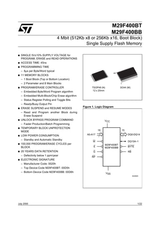
  • 1. M29F400BT M29F400BB 4 Mbit (512Kb x8 or 256Kb x16, Boot Block) Single Supply Flash Memory s SINGLE 5V±10% SUPPLY VOLTAGE for PROGRAM, ERASE and READ OPERATIONS s ACCESS TIME: 45ns s PROGRAMMING TIME – 8µs per Byte/Word typical 44 s 11 MEMORY BLOCKS – 1 Boot Block (Top or Bottom Location) – 2 Parameter and 8 Main Blocks 1 s PROGRAM/ERASE CONTROLLER TSOP48 (N) SO44 (M) – Embedded Byte/Word Program algorithm 12 x 20mm – Embedded Multi-Block/Chip Erase algorithm – Status Register Polling and Toggle Bits – Ready/Busy Output Pin Figure 1. Logic Diagram s ERASE SUSPEND and RESUME MODES – Read and Program another Block during Erase Suspend s UNLOCK BYPASS PROGRAM COMMAND VCC – Faster Production/Batch Programming s TEMPORARY BLOCK UNPROTECTION 18 15 MODE s LOW POWER CONSUMPTION A0-A17 DQ0-DQ14 – Standby and Automatic Standby W DQ15A–1 s 100,000 PROGRAM/ERASE CYCLES per M29F400BT BLOCK E M29F400BB BYTE s 20 YEARS DATA RETENTION G RB – Defectivity below 1 ppm/year RP s ELECTRONIC SIGNATURE – Manufacturer Code: 0020h – Top Device Code M29F400BT: 00D5h – Bottom Device Code M29F400BB: 00D6h VSS AI02904 July 2000 1/22
  • 2. M29F400BT, M29F400BB Figure 2. TSOP Connections Figure 3. SO Connections A15 1 48 A16 A14 BYTE NC 1 44 RP A13 VSS RB 2 43 W A12 DQ15A–1 A17 3 42 A8 A11 DQ7 A7 4 41 A9 A10 DQ14 A6 5 40 A10 A9 DQ6 A5 6 39 A11 A8 DQ13 A4 7 38 A12 NC DQ5 A3 8 37 A13 NC DQ12 A2 9 36 A14 W DQ4 A1 10 35 A15 RP 12 37 VCC A0 11 M29F400BT 34 A16 M29F400BT NC 13 M29F400BB 36 DQ11 E 12 M29F400BB 33 BYTE NC DQ3 VSS 13 32 VSS RB DQ10 G 14 31 DQ15A–1 NC DQ2 DQ0 15 30 DQ7 A17 DQ9 DQ8 16 29 DQ14 A7 DQ1 DQ1 17 28 DQ6 A6 DQ8 DQ9 18 27 DQ13 A5 DQ0 DQ2 19 26 DQ5 A4 G DQ10 20 25 DQ12 A3 VSS DQ3 21 24 DQ4 A2 E DQ11 22 23 VCC AI02906 A1 24 25 A0 AI02905 Table 1. Signal Names SUMMARY DESCRIPTION A0-A17 Address Inputs The M29F400B is a 4 Mbit (512Kb x8 or 256Kb x16) non-volatile memory that can be read, erased DQ0-DQ7 Data Inputs/Outputs and reprogrammed. These operations can be per- formed using a single 5V supply. On power-up the DQ8-DQ14 Data Inputs/Outputs memory defaults to its Read mode where it can be read in the same way as a ROM or EPROM. The DQ15A–1 Data Input/Output or Address Input M29F400B is fully backward compatible with the M29F400. E Chip Enable The memory is divided into blocks that can be G Output Enable erased independently so it is possible to preserve valid data while old data is erased. Each block can W Write Enable be protected independently to prevent accidental Program or Erase commands from modifying the RP Reset/Block Temporary Unprotect memory. Program and Erase commands are writ- ten to the Command Interface of the memory. An RB Ready/Busy Output on-chip Program/Erase Controller simplifies the process of programming or erasing the memory by BYTE Byte/Word Organization Select taking care of all of the special operations that are required to update the memory contents. The end VCC Supply Voltage of a program or erase operation can be detected and any error conditions identified. The command VSS Ground set required to control the memory is consistent with JEDEC standards. NC Not Connected Internally 2/22
  • 3. M29F400BT, M29F400BB Table 2. Absolute Maximum Ratings (1) Symbol Parameter Value Unit Ambient Operating Temperature (Temperature Range Option 1) 0 to 70 °C TA Ambient Operating Temperature (Temperature Range Option 6) –40 to 85 °C Ambient Operating Temperature (Temperature Range Option 3) –40 to 125 °C TBIAS Temperature Under Bias –50 to 125 °C TSTG Storage Temperature –65 to 150 °C VIO (2) Input or Output Voltage –0.6 to 6 V VCC Supply Voltage –0.6 to 6 V VID Identification Voltage –0.6 to 13.5 V Note: 1. Except for the rating "Operating Temperature Range", stresses above those listed in the Table "Absolute Maximum Ratings" may cause permanent damage to the device. These are stress ratings only and operation of the device at these or any other conditions above those indicated in the Operating sections of this specification is not implied. Exposure to Absolute Maximum Rating condi- tions for extended periods may affect device reliability. Refer also to the STMicroelectronics SURE Program and other relevant qual- ity documents. 2. Minimum Voltage may undershoot to –2V during transition and for less than 20ns during transitions. The blocks in the memory are asymmetrically ar- Chip Enable, Output Enable and Write Enable sig- ranged, see Tables 3 and 4, Block Addresses. The nals control the bus operation of the memory. first or last 64 Kbytes have been divided into four They allow simple connection to most micropro- additional blocks. The 16 Kbyte Boot Block can be cessors, often without additional logic. used for small initialization code to start the micro- The memory is offered in TSOP48 (12 x 20mm) processor, the two 8 Kbyte Parameter Blocks can and SO44 packages and it is supplied with all the be used for parameter storage and the remaining bits erased (set to ’1’). 32K is a small Main Block where the application may be stored. Table 3. Top Boot Block Addresses, Table 4. Bottom Boot Block addresses, M29F400BT M29F400BB Size Size Address Range Address Range Address Range Address Range # (Kbyte # (Kbyte (x8) (x16) (x8) (x16) s) s) 10 16 7C000h-7FFFFh 3E000h-3FFFFh 10 64 70000h-7FFFFh 38000h-3FFFFh 9 8 7A000h-7BFFFh 3D000h-3DFFFh 9 64 60000h-6FFFFh 30000h-37FFFh 8 8 78000h-79FFFh 3C000h-3CFFFh 8 64 50000h-5FFFFh 28000h-2FFFFh 7 32 70000h-77FFFh 38000h-3BFFFh 7 64 40000h-4FFFFh 20000h-27FFFh 6 64 60000h-6FFFFh 30000h-37FFFh 6 64 30000h-3FFFFh 18000h-1FFFFh 5 64 50000h-5FFFFh 28000h-2FFFFh 5 64 20000h-2FFFFh 10000h-17FFFh 4 64 40000h-4FFFFh 20000h-27FFFh 4 64 10000h-1FFFFh 08000h-0FFFFh 3 64 30000h-3FFFFh 18000h-1FFFFh 3 32 08000h-0FFFFh 04000h-07FFFh 2 64 20000h-2FFFFh 10000h-17FFFh 2 8 06000h-07FFFh 03000h-03FFFh 1 64 10000h-1FFFFh 08000h-0FFFFh 1 8 04000h-05FFFh 02000h-02FFFh 0 64 00000h-0FFFFh 00000h-07FFFh 0 16 00000h-03FFFh 00000h-01FFFh 3/22
  • 4. M29F400BT, M29F400BB SIGNAL DESCRIPTIONS tRHEL, whichever occurs last. See the Ready/Busy See Figure 1, Logic Diagram, and Table 1, Signal Output section, Table 17 and Figure 11, Reset/ Names, for a brief overview of the signals connect- Temporary Unprotect AC Characteristics for more ed to this device. details. Address Inputs (A0-A17). The Address Inputs Holding RP at V ID will temporarily unprotect the select the cells in the memory array to access dur- protected Blocks in the memory. Program and ing Bus Read operations. During Bus Write opera- Erase operations on all blocks will be possible. tions they control the commands sent to the The transition from VIH to VID must be slower than Command Interface of the internal state machine. tPHPHH. Data Inputs/Outputs (DQ0-DQ7). The Data In- Ready/Busy Output (RB). The Ready/Busy pin puts/Outputs output the data stored at the selected is an open-drain output that can be used to identify address during a Bus Read operation. During Bus when the memory array can be read. Ready/Busy Write operations they represent the commands is high-impedance during Read mode, Auto Select sent to the Command Interface of the internal state mode and Erase Suspend mode. machine. After a Hardware Reset, Bus Read and Bus Write Data Inputs/Outputs (DQ8-DQ14). The Data In- operations cannot begin until Ready/Busy be- puts/Outputs output the data stored at the selected comes high-impedance. See Table 17 and Figure address during a Bus Read operation when BYTE 11, Reset/Temporary Unprotect AC Characteris- is High, VIH. When BYTE is Low, VIL, these pins tics. are not used and are high impedance. During Bus During Program or Erase operations Ready/Busy Write operations the Command Register does not is Low, VOL. Ready/Busy will remain Low during use these bits. When reading the Status Register Read/Reset commands or Hardware Resets until these bits should be ignored. the memory is ready to enter Read mode. Data Input/Output or Address Input (DQ15A-1). The use of an open-drain output allows the Ready/ When BYTE is High, VIH, this pin behaves as a Busy pins from several memories to be connected Data Input/Output pin (as DQ8-DQ14). When to a single pull-up resistor. A Low will then indicate BYTE is Low, VIL, this pin behaves as an address that one, or more, of the memories is busy. pin; DQ15A–1 Low will select the LSB of the Word Byte/Word Organization Select (BYTE). The Byte/ on the other addresses, DQ15A–1 High will select Word Organization Select pin is used to switch be- the MSB. Throughout the text consider references tween the 8-bit and 16-bit Bus modes of the mem- to the Data Input/Output to include this pin when ory. When Byte/Word Organization Select is Low, BYTE is High and references to the Address In- VIL, the memory is in 8-bit mode, when it is High, puts to include this pin when BYTE is Low except VIH, the memory is in 16-bit mode. when stated explicitly otherwise. VCC Supply Voltage. The VCC Supply Voltage Chip Enable (E). The Chip Enable, E, activates supplies the power for all operations (Read, Pro- the memory, allowing Bus Read and Bus Write op- gram, Erase etc.). erations to be performed. When Chip Enable is The Command Interface is disabled when the V CC High, V IH, all other pins are ignored. Supply Voltage is less than the Lockout Voltage, Output Enable (G). The Output Enable, G, con- VLKO. This prevents Bus Write operations from ac- trols the Bus Read operation of the memory. cidentally damaging the data during power up, Write Enable (W). The Write Enable, W, controls power down and power surges. If the Program/ the Bus Write operation of the memory’s Com- Erase Controller is programming or erasing during mand Interface. this time then the operation aborts and the memo- ry contents being altered will be invalid. Reset/Block Temporary Unprotect (RP). The Re- set/Block Temporary Unprotect pin can be used to A 0.1µF capacitor should be connected between apply a Hardware Reset to the memory or to tem- the V CC Supply Voltage pin and the VSS Ground porarily unprotect all Blocks that have been pro- pin to decouple the current surges from the power tected. supply. The PCB track widths must be sufficient to carry the currents required during program and A Hardware Reset is achieved by holding Reset/ erase operations, ICC4. Block Temporary Unprotect Low, V IL, for at least tPLPX. After Reset/Block Temporary Unprotect Vss Ground. The VSS Ground is the reference goes High, V IH, the memory will be ready for Bus for all voltage measurements. Read and Bus Write operations after tPHEL or 4/22
  • 5. M29F400BT, M29F400BB BUS OPERATIONS mand Interface on the rising edge of Chip Enable There are five standard bus operations that control or Write Enable, whichever occurs first. Output En- the device. These are Bus Read, Bus Write, Out- able must remain High, VIH, during the whole Bus put Disable, Standby and Automatic Standby. See Write operation. See Figures 9 and 10, Write AC Tables 5 and 6, Bus Operations, for a summary. Waveforms, and Tables 15 and 16, Write AC Typically glitches of less than 5ns on Chip Enable Characteristics, for details of the timing require- or Write Enable are ignored by the memory and do ments. not affect bus operations. Output Disable. The Data Inputs/Outputs are in Bus Read. Bus Read operations read from the the high impedance state when Output Enable is memory cells, or specific registers in the Com- High, V IH. mand Interface. A valid Bus Read operation in- Standby. When Chip Enable is High, VIH, the volves setting the desired address on the Address Data Inputs/Outputs pins are placed in the high- Inputs, applying a Low signal, V IL, to Chip Enable impedance state and the Supply Current is re- and Output Enable and keeping Write Enable duced to the Standby level. High, VIH. The Data Inputs/Outputs will output the When Chip Enable is at V IH the Supply Current is value, see Figure 8, Read Mode AC Waveforms, reduced to the TTL Standby Supply Current, I CC2. and Table 14, Read AC Characteristics, for details To further reduce the Supply Current to the CMOS of when the output becomes valid. Standby Supply Current, ICC3, Chip Enable should Bus Write. Bus Write operations write to the be held within V CC ± 0.2V. For Standby current Command Interface. A valid Bus Write operation levels see Table 13, DC Characteristics. begins by setting the desired address on the Ad- During program or erase operations the memory dress Inputs. The Address Inputs are latched by will continue to use the Program/Erase Supply the Command Interface on the falling edge of Chip Current, ICC4, for Program or Erase operations un- Enable or Write Enable, whichever occurs last. til the operation completes. The Data Inputs/Outputs are latched by the Com- Table 5. Bus Operations, BYTE = V IL Address Inputs Data Inputs/Outputs Operation E G W DQ15A–1, A0-A17 DQ14-DQ8 DQ7-DQ0 Bus Read VIL VIL VIH Cell Address Hi-Z Data Output Bus Write VIL VIH VIL Command Address Hi-Z Data Input Output Disable X VIH VIH X Hi-Z Hi-Z Standby VIH X X X Hi-Z Hi-Z Read Manufacturer A0 = VIL, A1 = VIL, A9 = VID, VIL VIL VIH Hi-Z 20h Code Others VIL or VIH A0 = VIH, A1 = VIL, A9 = VID, D5h (M29F400BT) Read Device Code VIL VIL VIH Hi-Z Others VIL or VIH D6h (M29F400BB) Note: X = VIL or VIH. Table 6. Bus Operations, BYTE = V IH Address Inputs Data Inputs/Outputs Operation E G W A0-A17 DQ15A–1, DQ14-DQ0 Bus Read VIL VIL VIH Cell Address Data Output Bus Write VIL VIH VIL Command Address Data Input Output Disable X VIH VIH X Hi-Z Standby VIH X X X Hi-Z Read Manufacturer A0 = VIL, A1 = VIL, A9 = VID, VIL VIL VIH 0020h Code Others VIL or VIH A0 = VIH, A1 = VIL, A9 = VID, 00D5h (M29F400BT) Read Device Code VIL VIL VIH Others VIL or VIH 00D6h (M29F400BB) Note: X = VIL or VIH. 5/22
  • 6. M29F400BT, M29F400BB Automatic Standby. If CMOS levels (VCC ± 0.2V) COMMAND INTERFACE are used to drive the bus and the bus is inactive for All Bus Write operations to the memory are inter- 150ns or more the memory enters Automatic preted by the Command Interface. Commands Standby where the internal Supply Current is re- consist of one or more sequential Bus Write oper- duced to the CMOS Standby Supply Current, ICC3. ations. Failure to observe a valid sequence of Bus The Data Inputs/Outputs will still output data if a Write operations will result in the memory return- Bus Read operation is in progress. ing to Read mode. The long command sequences Special Bus Operations are imposed to maximize data security. Additional bus operations can be performed to The address used for the commands changes de- read the Electronic Signature and also to apply pending on whether the memory is in 16-bit or 8- and remove Block Protection. These bus opera- bit mode. See either Table 7, or 8, depending on tions are intended for use by programming equip- the configuration that is being used, for a summary ment and are not usually used in applications. of the commands. They require VID to be applied to some pins. Read/Reset Command. The Read/Reset com- Electronic Signature. The memory has two mand returns the memory to its Read mode where codes, the manufacturer code and the device it behaves like a ROM or EPROM. It also resets code, that can be read to identify the memory. the errors in the Status Register. Either one or These codes can be read by applying the signals three Bus Write operations can be used to issue listed in Tables 5 and 6, Bus Operations. the Read/Reset command. Block Protection and Blocks Unprotection. Each If the Read/Reset command is issued during a block can be separately protected against acci- Block Erase operation or following a Programming dental Program or Erase. Protected blocks can be or Erase error then the memory will take upto 10µs unprotected to allow data to be changed. to abort. During the abort period no valid data can There are two methods available for protecting be read from the memory. Issuing a Read/Reset and unprotecting the blocks, one for use on pro- command during a Block Erase operation will gramming equipment and the other for in-system leave invalid data in the memory. use. For further information refer to Application Auto Select Command. The Auto Select com- Note AN1122, Applying Protection and Unprotec- mand is used to read the Manufacturer Code, the tion to M29 Series Flash. Device Code and the Block Protection Status. Three consecutive Bus Write operations are re- quired to issue the Auto Select command. Once the Auto Select command is issued the memory remains in Auto Select mode until another com- mand is issued. From the Auto Select mode the Manufacturer Code can be read using a Bus Read operation with A0 = V IL and A1 = VIL. The other address bits may be set to either V IL or VIH. The Manufacturer Code for STMicroelectronics is 0020h. The Device Code can be read using a Bus Read operation with A0 = VIH and A1 = VIL. The other address bits may be set to either V IL or VIH. The Device Code for the M29F400BT is 00D5h and for the M29F400BB is 00D6h. 6/22
  • 7. M29F400BT, M29F400BB Table 7. Commands, 16-bit mode, BYTE = VIH Bus Write Operations Length Command 1st 2nd 3rd 4th 5th 6th Addr Data Addr Data Addr Data Addr Data Addr Data Addr Data 1 X F0 Read/Reset 3 555 AA 2AA 55 X F0 Auto Select 3 555 AA 2AA 55 555 90 Program 4 555 AA 2AA 55 555 A0 PA PD Unlock Bypass 3 555 AA 2AA 55 555 20 Unlock Bypass 2 X A0 PA PD Program Unlock Bypass Reset 2 X 90 X 00 Chip Erase 6 555 AA 2AA 55 555 80 555 AA 2AA 55 555 10 Block Erase 6+ 555 AA 2AA 55 555 80 555 AA 2AA 55 BA 30 Erase Suspend 1 X B0 Erase Resume 1 X 30 Table 8. Commands, 8-bit mode, BYTE = VIL Bus Write Operations Length Command 1st 2nd 3rd 4th 5th 6th Addr Data Addr Data Addr Data Addr Data Addr Data Addr Data 1 X F0 Read/Reset 3 AAA AA 555 55 X F0 Auto Select 3 AAA AA 555 55 AAA 90 Program 4 AAA AA 555 55 AAA A0 PA PD Unlock Bypass 3 AAA AA 555 55 AAA 20 Unlock Bypass 2 X A0 PA PD Program Unlock Bypass Reset 2 X 90 X 00 Chip Erase 6 AAA AA 555 55 AAA 80 AAA AA 555 55 AAA 10 Block Erase 6+ AAA AA 555 55 AAA 80 AAA AA 555 55 BA 30 Erase Suspend 1 X B0 Erase Resume 1 X 30 Note: X Don’t Care, PA Program Address, PD Program Data, BA Any address in the Block. All values in the table are in hexadecimal. The Command Interface only uses A–1, A0-A10 and DQ0-DQ7 to verify the commands; A11-A17, DQ8-DQ14 and DQ15 are Don’t Care. DQ15A–1 is A–1 when BYTE is VIL or DQ15 when BYTE is VIH . Read/Reset. After a Read/Reset command, read the memory as normal until another command is issued. Auto Select. After an Auto Select command, read Manufacturer ID, Device ID or Block Protection Status. Program, Unlock Bypass Program, Chip Erase, Block Erase. After these commands read the Status Register until the Program/Erase Controller completes and the memory returns to Read Mode. Add additional Blocks during Block Erase Command with additional Bus Write Operations until Timeout Bit is set. Unlock Bypass. After the Unlock Bypass command issue Unlock Bypass Program or Unlock Bypass Reset commands. Unlock Bypass Reset. After the Unlock Bypass Reset command read the memory as normal until another command is issued. Erase Suspend. After the Erase Suspend command read non-erasing memory blocks as normal, issue Auto Select and Program commands on non-erasing blocks as normal. Erase Resume. After the Erase Resume command the suspended Erase operation resumes, read the Status Register until the Program/ Erase Controller completes and the memory returns to Read Mode. 7/22
  • 8. M29F400BT, M29F400BB The Block Protection Status of each block can be Unlock Bypass Program Command. The Un- read using a Bus Read operation with A0 = VIL, lock Bypass Program command can be used to A1 = VIH, and A12-A17 specifying the address of program one address in memory at a time. The the block. The other address bits may be set to ei- command requires two Bus Write operations, the ther VIL or VIH. If the addressed block is protected final write operation latches the address and data then 01h is output on Data Inputs/Outputs DQ0- in the internal state machine and starts the Pro- DQ7, otherwise 00h is output. gram/Erase Controller. Program Command. The Program command The Program operation using the Unlock Bypass can be used to program a value to one address in Program command behaves identically to the Pro- the memory array at a time. The command re- gram operation using the Program command. A quires four Bus Write operations, the final write op- protected block cannot be programmed; the oper- eration latches the address and data in the internal ation cannot be aborted and the Status Register is state machine and starts the Program/Erase Con- read. Errors must be reset using the Read/Reset troller. command, which leaves the device in Unlock By- If the address falls in a protected block then the pass Mode. See the Program command for details Program command is ignored, the data remains on the behavior. unchanged. The Status Register is never read and Unlock Bypass Reset Command. The Unlock no error condition is given. Bypass Reset command can be used to return to During the program operation the memory will ig- Read/Reset mode from Unlock Bypass Mode. nore all commands. It is not possible to issue any Two Bus Write operations are required to issue the command to abort or pause the operation. Typical Unlock Bypass Reset command. program times are given in Table 9. Bus Read op- Chip Erase Command. The Chip Erase com- erations during the program operation will output mand can be used to erase the entire chip. Six Bus the Status Register on the Data Inputs/Outputs. Write operations are required to issue the Chip See the section on the Status Register for more Erase Command and start the Program/Erase details. Controller. After the program operation has completed the If any blocks are protected then these are ignored memory will return to the Read mode, unless an and all the other blocks are erased. If all of the error has occurred. When an error occurs the blocks are protected the Chip Erase operation ap- memory will continue to output the Status Regis- pears to start but will terminate within about 100µs, ter. A Read/Reset command must be issued to re- leaving the data unchanged. No error condition is set the error condition and return to Read mode. given when protected blocks are ignored. Note that the Program command cannot change a During the erase operation the memory will ignore bit set at ’0’ back to ’1’. One of the Erase Com- all commands. It is not possible to issue any com- mands must be used to set all the bits in a block or mand to abort the operation. Typical chip erase in the whole memory from ’0’ to ’1’. times are given in Table 9. All Bus Read opera- Unlock Bypass Command. The Unlock Bypass tions during the Chip Erase operation will output command is used in conjunction with the Unlock the Status Register on the Data Inputs/Outputs. Bypass Program command to program the memo- See the section on the Status Register for more ry. When the access time to the device is long (as details. with some EPROM programmers) considerable After the Chip Erase operation has completed the time saving can be made by using these com- memory will return to the Read Mode, unless an mands. Three Bus Write operations are required error has occurred. When an error occurs the to issue the Unlock Bypass command. memory will continue to output the Status Regis- Once the Unlock Bypass command has been is- ter. A Read/Reset command must be issued to re- sued the memory will only accept the Unlock By- set the error condition and return to Read Mode. pass Program command and the Unlock Bypass The Chip Erase Command sets all of the bits in un- Reset command. The memory can be read as if in protected blocks of the memory to ’1’. All previous Read mode. data is lost. 8/22
  • 9. M29F400BT, M29F400BB Block Erase Command. The Block Erase com- ter. A Read/Reset command must be issued to re- mand can be used to erase a list of one or more set the error condition and return to Read mode. blocks. Six Bus Write operations are required to The Block Erase Command sets all of the bits in select the first block in the list. Each additional the unprotected selected blocks to ’1’. All previous block in the list can be selected by repeating the data in the selected blocks is lost. sixth Bus Write operation using the address of the additional block. The Block Erase operation starts Erase Suspend Command. The Erase Suspend Command may be used to temporarily suspend a the Program/Erase Controller about 50µs after the Block Erase operation and return the memory to last Bus Write operation. Once the Program/Erase Controller starts it is not possible to select any Read mode. The command requires one Bus more blocks. Each additional block must therefore Write operation. be selected within 50µs of the last block. The 50µs The Program/Erase Controller will suspend within timer restarts when an additional block is selected. 15µs of the Erase Suspend Command being is- The Status Register can be read after the sixth sued. Once the Program/Erase Controller has Bus Write operation. See the Status Register for stopped the memory will be set to Read mode and details on how to identify if the Program/Erase the Erase will be suspended. If the Erase Suspend Controller has started the Block Erase operation. command is issued during the period when the If any selected blocks are protected then these are memory is waiting for an additional block (before ignored and all the other selected blocks are the Program/Erase Controller starts) then the Erase is suspended immediately and will start im- erased. If all of the selected blocks are protected mediately when the Erase Resume Command is the Block Erase operation appears to start but will terminate within about 100µs, leaving the data un- issued. It will not be possible to select any further blocks for erasure after the Erase Resume. changed. No error condition is given when protect- ed blocks are ignored. During Erase Suspend it is possible to Read and Program cells in blocks that are not being erased; During the Block Erase operation the memory will ignore all commands except the Erase Suspend both Read and Program operations behave as and Read/Reset commands. Typical block erase normal on these blocks. Reading from blocks that are being erased will output the Status Register. It times are given in Table 9. All Bus Read opera- is also possible to enter the Auto Select mode: the tions during the Block Erase operation will output the Status Register on the Data Inputs/Outputs. memory will behave as in the Auto Select mode on all blocks until a Read/Reset command returns the See the section on the Status Register for more memory to Erase Suspend mode. details. Erase Resume Command. The Erase Resume After the Block Erase operation has completed the command must be used to restart the Program/ memory will return to the Read Mode, unless an error has occurred. When an error occurs the Erase Controller from Erase Suspend. An erase can be suspended and resumed more than once. memory will continue to output the Status Regis- Table 9. Program, Erase Times and Program, Erase Endurance Cycles (TA = 0 to 70°C, –40 to 85°C or –40 to 125°C) Typical after Parameter Min Typ (1) Max Unit 100k W/E Cycles (1) Chip Erase (All bits in the memory set to ‘0’) 1.5 1.5 sec Chip Erase 5 5 20 sec Block Erase (64 Kbytes) 0.6 0.6 4 sec Program (Byte or Word) 8 8 150 µs Chip Program (Byte by Byte) 4.5 4.5 18 sec Chip Program (Word by Word) 2.3 2.3 9 sec Program/Erase Cycles (per Block) 100,000 cycles Note: 1. TA = 25°C, VCC = 5V. 9/22
  • 10. M29F400BT, M29F400BB STATUS REGISTER Toggle Bit (DQ6). The Toggle Bit can be used to Bus Read operations from any address always identify whether the Program/Erase Controller has read the Status Register during Program and successfully completed its operation or if it has re- Erase operations. It is also read during Erase Sus- sponded to an Erase Suspend. The Toggle Bit is pend when an address within a block being erased output on DQ6 when the Status Register is read. is accessed. During Program and Erase operations the Toggle The bits in the Status Register are summarized in Bit changes from ’0’ to ’1’ to ’0’, etc., with succes- Table 10, Status Register Bits. sive Bus Read operations at any address. After successful completion of the operation the memo- Data Polling Bit (DQ7). The Data Polling Bit can ry returns to Read mode. be used to identify whether the Program/Erase Controller has successfully completed its opera- During Erase Suspend mode the Toggle Bit will tion or if it has responded to an Erase Suspend. output when addressing a cell within a block being The Data Polling Bit is output on DQ7 when the erased. The Toggle Bit will stop toggling when the Status Register is read. Program/Erase Controller has suspended the Erase operation. During Program operations the Data Polling Bit outputs the complement of the bit being pro- Figure 5, Data Toggle Flowchart, gives an exam- grammed to DQ7. After successful completion of ple of how to use the Data Toggle Bit. the Program operation the memory returns to Error Bit (DQ5). The Error Bit can be used to Read mode and Bus Read operations from the ad- identify errors detected by the Program/Erase dress just programmed output DQ7, not its com- Controller. The Error Bit is set to ’1’ when a Pro- plement. gram, Block Erase or Chip Erase operation fails to During Erase operations the Data Polling Bit out- write the correct data to the memory. If the Error puts ’0’, the complement of the erased state of Bit is set a Read/Reset command must be issued DQ7. After successful completion of the Erase op- before other commands are issued. The Error bit eration the memory returns to Read Mode. is output on DQ5 when the Status Register is read. In Erase Suspend mode the Data Polling Bit will Note that the Program command cannot change a output a ’1’ during a Bus Read operation within a bit set at ’0’ back to ’1’ and attempting to do so may block being erased. The Data Polling Bit will or may not set DQ5 at ‘1’. In both cases, a succes- change from a ’0’ to a ’1’ when the Program/Erase sive Bus Read operation will show the bit is still ‘0’. Controller has suspended the Erase operation. One of the Erase commands must be used to set all the bits in a block or in the whole memory from Figure 4, Data Polling Flowchart, gives an exam- ’0’ to ’1’. ple of how to use the Data Polling Bit. A Valid Ad- dress is the address being programmed or an address within the block being erased. Table 10. Status Register Bits Operation Address DQ7 DQ6 DQ5 DQ3 DQ2 RB Program Any Address DQ7 Toggle 0 – – 0 Program During Erase Any Address DQ7 Toggle 0 – – 0 Suspend Program Error Any Address DQ7 Toggle 1 – – 0 Chip Erase Any Address 0 Toggle 0 1 Toggle 0 Block Erase before Erasing Block 0 Toggle 0 0 Toggle 0 timeout Non-Erasing Block 0 Toggle 0 0 No Toggle 0 Erasing Block 0 Toggle 0 1 Toggle 0 Block Erase Non-Erasing Block 0 Toggle 0 1 No Toggle 0 Erasing Block 1 No Toggle 0 – Toggle 1 Erase Suspend Non-Erasing Block Data read as normal 1 Good Block Address 0 Toggle 1 1 No Toggle 0 Erase Error Faulty Block Address 0 Toggle 1 1 Toggle 0 Note: Unspecified data bits should be ignored. 10/22
  • 11. M29F400BT, M29F400BB Figure 4. Data Polling Flowchart Figure 5. Data Toggle Flowchart START START READ READ DQ5 & DQ7 DQ5 & DQ6 at VALID ADDRESS READ DQ6 DQ7 YES = DATA DQ6 NO = NO TOGGLE YES NO DQ5 =1 NO DQ5 YES =1 YES READ DQ7 at VALID ADDRESS READ DQ6 TWICE DQ7 YES = DATA DQ6 NO = TOGGLE NO YES FAIL PASS FAIL PASS AI03598 AI01370B Erase Timer Bit (DQ3). The Erase Timer Bit can within the blocks being erased. Once the operation be used to identify the start of Program/Erase completes the memory returns to Read mode. Controller operation during a Block Erase com- During Erase Suspend the Alternative Toggle Bit mand. Once the Program/Erase Controller starts changes from ’0’ to ’1’ to ’0’, etc. with successive erasing the Erase Timer Bit is set to ’1’. Before the Bus Read operations from addresses within the Program/Erase Controller starts the Erase Timer blocks being erased. Bus Read operations to ad- Bit is set to ’0’ and additional blocks to be erased dresses within blocks not being erased will output may be written to the Command Interface. The the memory cell data as if in Read mode. Erase Timer Bit is output on DQ3 when the Status After an Erase operation that causes the Error Bit Register is read. to be set the Alternative Toggle Bit can be used to Alternative Toggle Bit (DQ2). The Alternative identify which block or blocks have caused the er- Toggle Bit can be used to monitor the Program/ ror. The Alternative Toggle Bit changes from ’0’ to Erase controller during Erase operations. The Al- ’1’ to ’0’, etc. with successive Bus Read Opera- ternative Toggle Bit is output on DQ2 when the tions from addresses within blocks that have not Status Register is read. erased correctly. The Alternative Toggle Bit does During Chip Erase and Block Erase operations the not change if the addressed block has erased cor- Toggle Bit changes from ’0’ to ’1’ to ’0’, etc., with rectly. successive Bus Read operations from addresses 11/22
  • 12. M29F400BT, M29F400BB Table 11. AC Measurement Conditions M29F400B Parameter 45 / 55 70 / 90 AC Test Conditions High Speed Standard Load Capacitance (CL) 30pF 100pF Input Rise and Fall Times ≤ 10ns ≤ 10ns Input Pulse Voltages 0 to 3V 0.45 to 2.4V Input and Output Timing Ref. Voltages 1.5V 0.8V and 2.0V Figure 6. AC Testing Input Output Waveform Figure 7. AC Testing Load Circuit 1.3V High Speed 1N914 3V 1.5V 0V 3.3kΩ DEVICE Standard UNDER OUT TEST 2.4V CL = 30pF or 100pF 2.0V 0.8V 0.45V AI01275B CL includes JIG capacitance AI03027 Table 12. Capacitance (TA = 25 °C, f = 1 MHz) Symbol Parameter Test Condition Min Max Unit CIN Input Capacitance VIN = 0V 6 pF COUT Output Capacitance VOUT = 0V 12 pF Note: Sampled only, not 100% tested. 12/22
  • 13. M29F400BT, M29F400BB Table 13. DC Characteristics (TA = 0 to 70°C, –40 to 85°C or –40 to 125°C) Symbol Parameter Test Condition Min Typ. (2) Max Unit ILI Input Leakage Current 0V ≤ VIN ≤ VCC ±1 µA ILO Output Leakage Current 0V ≤ VOUT ≤ VCC ±1 µA ICC1 Supply Current (Read) E = VIL, G = VIH, f = 6MHz 7 20 mA ICC2 Supply Current (Standby) TTL E = VIH 1 mA E = VCC ±0.2V, ICC3 Supply Current (Standby) CMOS RP = VCC ±0.2V 30 100 µA Program/Erase ICC4 (1) Supply Current (Program/Erase) 20 mA Controller active VIL Input Low Voltage –0.5 0.8 V VIH Input High Voltage 2 VCC +0.5 V VOL Output Low Voltage IOL = 5.8mA 0.45 V Output High Voltage TTL IOH = –2.5mA 2.4 V VOH Output High Voltage CMOS IOH = –100µ A VCC –0.4 V VID Identification Voltage 11.5 12.5 V IID Identification Current A9 = VID 100 µA Program/Erase Lockout Supply VLKO (1) 3.2 4.2 V Voltage Note: 1. Sampled only, not 100% tested. 2. TA = 25 °C, VCC = 5V. 13/22
  • 14. M29F400BT, M29F400BB Table 14. Read AC Characteristics (TA = 0 to 70°C, –40 to 85°C or –40 to 125°C) M29F400B Symbol Alt Parameter Test Condition Unit 45 55 70 / 90 E = VIL, tAVAV tRC Address Valid to Next Address Valid Min 45 55 70 ns G = VIL E = VIL, tAVQV tACC Address Valid to Output Valid Max 45 55 70 ns G = VIL Chip Enable Low to Output tELQX (1) tLZ G = VIL Min 0 0 0 ns Transition tELQV tCE Chip Enable Low to Output Valid G = VIL Max 45 55 70 ns Output Enable Low to Output tGLQX (1) tOLZ E = VIL Min 0 0 0 ns Transition tGLQV tOE Output Enable Low to Output Valid E = VIL Max 25 30 30 ns tEHQZ (1) tHZ Chip Enable High to Output Hi-Z G = VIL Max 15 18 20 ns tGHQZ (1) tDF Output Enable High to Output Hi-Z E = VIL Max 15 18 20 ns tEHQX Chip Enable, Output Enable or tGHQX tOH Address Transition to Output Min 0 0 0 ns tAXQX Transition tELBL tELFL Chip Enable to BYTE Low or High Max 5 5 5 ns tELBH tELFH tBLQZ tFLQZ BYTE Low to Output Hi-Z Max 15 15 20 ns tBHQV tFHQV BYTE High to Output Valid Max 30 30 30 ns Note: 1. Sampled only, not 100% tested. Figure 8. Read Mode AC Waveforms tAVAV A0-A17/ VALID A–1 tAVQV tAXQX E tELQV tEHQX tELQX tEHQZ G tGLQX tGHQX tGLQV tGHQZ DQ0-DQ7/ VALID DQ8-DQ15 tBHQV BYTE tELBL/tELBH tBLQZ AI02907 14/22
  • 15. M29F400BT, M29F400BB Table 15. Write AC Characteristics, Write Enable Controlled (TA = 0 to 70 °C, –40 to 85 °C or –40 to 125 °C) M29F400B Symbol Alt Parameter Unit 45 55 70 / 90 tAVAV tWC Address Valid to Next Address Valid Min 45 55 70 ns tELWL tCS Chip Enable Low to Write Enable Low Min 0 0 0 ns tWLWH tWP Write Enable Low to Write Enable High Min 40 40 45 ns tDVWH tDS Input Valid to Write Enable High Min 25 25 30 ns tWHDX tDH Write Enable High to Input Transition Min 0 0 0 ns tWHEH tCH Write Enable High to Chip Enable High Min 0 0 0 ns tWHWL tWPH Write Enable High to Write Enable Low Min 20 20 20 ns tAVWL tAS Address Valid to Write Enable Low Min 0 0 0 ns tWLAX tAH Write Enable Low to Address Transition Min 40 40 45 ns tGHWL Output Enable High to Write Enable Low Min 0 0 0 ns tWHGL tOEH Write Enable High to Output Enable Low Min 0 0 0 ns tWHRL (1) tBUSY Program/Erase Valid to RB Low Max 30 30 30 ns tVCHEL tVCS VCC High to Chip Enable Low Min 50 50 50 µs Note: 1. Sampled only, not 100% tested. Figure 9. Write AC Waveforms, Write Enable Controlled tAVAV A0-A17/ VALID A–1 tWLAX tAVWL tWHEH E tELWL tWHGL G tGHWL tWLWH W tWHWL tDVWH tWHDX DQ0-DQ7/ VALID DQ8-DQ15 VCC tVCHEL RB tWHRL AI01869C 15/22
  • 16. M29F400BT, M29F400BB Table 16. Write AC Characteristics, Chip Enable Controlled (TA = 0 to 70 °C, –40 to 85 °C or –40 to 125 °C) M29F400B Symbol Alt Parameter Unit 45 55 70 / 90 tAVAV tWC Address Valid to Next Address Valid Min 45 55 70 ns tWLEL tWS Write Enable Low to Chip Enable Low Min 0 0 0 ns tELEH tCP Chip Enable Low to Chip Enable High Min 40 40 45 ns tDVEH tDS Input Valid to Chip Enable High Min 25 25 30 ns tEHDX tDH Chip Enable High to Input Transition Min 0 0 0 ns tEHWH tWH Chip Enable High to Write Enable High Min 0 0 0 ns tEHEL tCPH Chip Enable High to Chip Enable Low Min 20 20 20 ns tAVEL tAS Address Valid to Chip Enable Low Min 0 0 0 ns tELAX tAH Chip Enable Low to Address Transition Min 40 40 45 ns tGHEL Output Enable High Chip Enable Low Min 0 0 0 ns tEHGL tOEH Chip Enable High to Output Enable Low Min 0 0 0 ns tEHRL (1) tBUSY Program/Erase Valid to RB Low Max 30 30 30 ns tVCHWL tVCS VCC High to Write Enable Low Min 50 50 50 µs Note: 1. Sampled only, not 100% tested. Figure 10. Write AC Waveforms, Chip Enable Controlled tAVAV A0-A17/ VALID A–1 tELAX tAVEL tEHWH W tWLEL tEHGL G tGHEL tELEH E tEHEL tDVEH tEHDX DQ0-DQ7/ VALID DQ8-DQ15 VCC tVCHWL RB tEHRL AI01870C 16/22
  • 17. M29F400BT, M29F400BB Table 17. Reset/Block Temporary Unprotect AC Characteristics (TA = 0 to 70 °C, –40 to 85 °C or –40 to 125 °C) M29F400B Symbol Alt Parameter Unit 45 55 70 / 90 tPHWL (1) RP High to Write Enable Low, Chip Enable tPHEL tRH Min 50 50 50 ns (1) Low, Output Enable Low tPHGL tRHWL (1) RB High to Write Enable Low, Chip Enable tRHEL (1) tRB Min 0 0 0 ns Low, Output Enable Low (1) tRHGL tPLPX tRP RP Pulse Width Min 500 500 500 ns tPLYH (1) tREADY RP Low to Read Mode Max 10 10 10 µs tPHPHH (1) tVIDR RP Rise Time to VID Min 500 500 500 ns Note: 1. Sampled only, not 100% tested. Figure 11. Reset/Block Temporary Unprotect AC Waveforms W, E, G tPHWL, tPHEL, tPHGL RB tRHWL, tRHEL, tRHGL tPLPX RP tPHPHH tPLYH AI02931 17/22
  • 18. M29F400BT, M29F400BB Table 18. Ordering Information Scheme Example: M29F400BB 55 N 1 T Device Type M29 Operating Voltage F = VCC = 5V ± 10% Device Function 400B = 4 Mbit (512Kb x8 or 256Kb x16), Boot Block Array Matrix T = Top Boot B = Bottom Boot Speed 45 = 45 ns 55 = 55 ns 70 = 70 ns 90 = 90 ns Package N = TSOP48: 12 x 20 mm M = SO44 Temperature Range 1 = 0 to 70 °C 3 = –40 to 125 °C 6 = –40 to 85 °C Option T = Tape & Reel Packing Note: The last two characters of the ordering code may be replaced by a letter code for preprogrammed parts, otherwise devices are shipped from the factory with the memory content bits erased to ‘1’. For a list of available options (Speed, Package, etc...) or for further information on any aspect of this de- vice, please contact the ST Sales Office nearest to you. 18/22
  • 19. M29F400BT, M29F400BB Table 19. Revision History Date Revision Details July 1999 First Issue Chip Erase Max. specification added (Table 9) Block Erase Max. specification added (Table 9) 09/21/99 Program Max. specification added (Table 9) Chip Program Max. specification added (Table 9) ICC1 and ICC3 Typ. specification added (Table 13) 10/04/99 ICC3 Test Condition change (Table 13) New document template Document type: from Preliminary Data to Data Sheet 07/28/00 Status Register bit DQ5 clarification Data Polling Flowchart diagram change (Figure 4) Data Toggle Flowchart diagram change (Figure 5) 19/22
  • 20. M29F400BT, M29F400BB Table 20. TSOP48 - 48 lead Plastic Thin Small Outline, 12 x 20mm, Package Mechanical Data mm inches Symbol Typ Min Max Typ Min Max A 1.20 0.0472 A1 0.05 0.15 0.0020 0.0059 A2 0.95 1.05 0.0374 0.0413 B 0.17 0.27 0.0067 0.0106 C 0.10 0.21 0.0039 0.0083 D 19.80 20.20 0.7795 0.7953 D1 18.30 18.50 0.7205 0.7283 E 11.90 12.10 0.4685 0.4764 e 0.50 – – 0.0197 – – L 0.50 0.70 0.0197 0.0279 α 0° 5° 0° 5° N 48 48 CP 0.10 0.0039 Figure 12. TSOP48 - 48 lead Plastic Thin Small Outline, 12 x 20mm, Package Outline A2 1 N e E B N/2 D1 A D CP DIE C TSOP-a A1 α L Drawing is not to scale. 20/22
  • 21. M29F400BT, M29F400BB Table 21. SO44 - 44 lead Plastic Small Outline, 525 mils body width, Package Mechanical Data mm inches Symbol Typ Min Max Typ Min Max A 2.42 2.62 0.0953 0.1031 A1 0.22 0.23 0.0087 0.0091 A2 2.25 2.35 0.0886 0.0925 B 0.50 0.0197 C 0.10 0.25 0.0039 0.0098 D 28.10 28.30 1.1063 1.1142 E 13.20 13.40 0.5197 0.5276 e 1.27 – – 0.0500 – – H 15.90 16.10 0.6260 0.6339 L 0.80 – – 0.0315 – – α 3° – – 3° – – N 44 44 CP 0.10 0.0039 Figure 13. SO44 - 44 lead Plastic Small Outline, 525 mils body width, Package Outline A2 A C B e CP D N E H 1 A1 α L SO-b Drawing is not to scale. 21/22
  • 22. M29F400BT, M29F400BB Information furnished is believed to be accurate and reliable. However, STMicroelectronics assumes no responsibility for the consequences of use of such information nor for any infringement of patents or other rights of third parties which may result from its use. No license is granted by implication or otherwise under any patent or patent rights of STMicroelectronics. Specifications mentioned in this publication are subject to change without notice. This publication supersedes and replaces all information previously supplied. STMicroelectronics products are not authorized for use as critical components in life support devices or systems without express written approval of STMicroelectronics. The ST logo is registered trademark of STMicroelectronics ® 2000 STMicroelectronics - All Rights Reserved All other names are the property of their respective owners. STMicroelectronics GROUP OF COMPANIES Australia - Brazil - China - Finland - France - Germany - Hong Kong - India - Italy - Japan - Malaysia - Malta - Morocco - Singapore - Spain - Sweden - Switzerland - United Kingdom - U.S.A. http://www.st.com 22/22