
Recomendados
Más contenido relacionado
Destacado
Destacado (16)
Similar a Things to come - possible futures for electronics
Similar a Things to come - possible futures for electronics (20)
Último
Último (20)
Things to come - possible futures for electronics
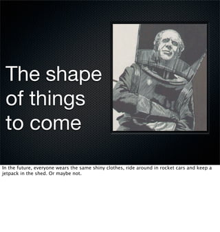
- 1. The shape of things to come In the future, everyone wears the same shiny clothes, ride around in rocket cars and keep a jetpack in the shed. Or maybe not.
- 2. Ray Kurzweil’s dream “The emergence in the early 21st Century of a new form of intelligence on Earth will be of greater import than any of the events that have shaped human history.” Ray Kurzweil, the inventor behind one of the most popular speech recognition packages and New Order’s favourite synthesiser, has a dream.
- 3. Kurzweil argues that computers will soon be able to replicate and ultimately surpass the performance of the human brain. Given that models of biological processes are still at an early stage, this prediction is likely to be a highly optimistic but the graph is important in another way. Kurzweil argues that Moore’s Law is simply one incarnation of a continuing exponential trend, and one that’s doing rather better than exponential when you consider this is meant to be a log-plot. Gordon Moore complains he’s become the father of exponentials when people talk about the Moore’s Law of disposable razors. But Moore’s eponymous law is, to Kurzweil, one step on the path to the Singularity, an event that may only ever exist in the inventor’s imagination.
- 4. The end of Moore’s Law... The electronics industry has more pressing matters: what happens when either the economics or physics of silicon-based semiconductors slam into the wall.
- 5. ...isn’t coming for a while The joke around the industry is that Moore’s Law might outlast Extreme UV lithogaphy. I can’t find anyone that reckons it stands a chance before 22nm, even though trying to draw features 20nm across using 193nm-wavelength light sounds crazy. Maybe as the feature size heads towards 10nm we will see a change in attitude but thanks to a new crop of workarounds appearing there is still some life left in today’s UV lithography. The big issue surrounding the future of Moore’s Law is how small you want to make a transistor. In 2003, NEC built an experimental 5nm transistor on bulk CMOS. It went from on to not quite so on, but it behaved more or less like a transistor. Since then, NEC has improved the design and demonstrated that a 5nm technology is at least possible. Variability is a big problem. At the same conference in mid-December 2008, CEA-LETI will talk about how they reduced threshold-voltage variability using FD-SOI. Again, the jury is out on whether the move to SOI is needed ultimately, but the option is still there.
- 6. The industry adapts to scaling problems almost transparently: Moore’s Law stays on track even though the underlying assumptions change. This graph is from Moore’s 1975 IEDM paper which went into more detail than the original 1965 Electronics article. At the time, yield improvements were making it possible to build larger and larger chips. Dimension reduction was comparatively unimportant. That changed during the 1980s.
- 7. Itanium Penryn 80486 Gradually, things dropped out of the Moore’s Law mix. The first to go was die size scaling. If scaling had followed the 1975 prediction, we would have been worrying about the 600mm2 area of the reticle by the mid-1990s.
- 8. Instead, process engineers took up the slack and allowed chipmakers to stay, more or less within the confines of 1cm, at least for high-volume products. The graph shows an analysis of chips made in the past 40 years or so, originally put together for an article in Engineering & Technology with most of the data coming from the annual ISSCC conferences or VLSI Symposia. The graph of transistor density shows how chipmakers started to accelerate the rate at which they introduced new processors as the increase in die size slowed and then stopped.
- 9. Another view of the same data shows what we expect from Moore’s Law: this shows the increase in transistor count since 1970 and you can fit a remarkably straight line to the data. A plot of high-volume, high-density devices is likely to be even more consistent. Behind the scenes, chipmakers have added more layers of metal, messed with the layout of memory cells and used a two-year update cycle in place of the slower progress of the 1970s and 1980s. But, this trend has to stop some time.
- 10. How costly are silicon fabs? Everyone talks about the escalating cost of fabs. Only a select few can afford to the build them. Yet, manufacturing cost is not going to kill off Moore’s Law just yet. Economies of scale have made it possible for fabs to spend no more per square metre of silicon than they did in the 1990s. Without the three near suicidal capacity-spend surges, which went nowhere, this graph would be far more consistent. The dark-blue line shows the conventional analysis of capital expenditure as a percentage of IC sales. With the light-blue line, I’ve taken an alternative approach: calculate how effective the spend has been in terms of wafer production. It shows, on the assumption that, on average, equipment purchases kick in up to 18 months later, a wafer start per week costs about $5000 in chipmaking kit. As it did at the start of the 1990s.
- 11. 10nm, 5nm: end of the line? It’s not clear when the music will stop. But there has to be a point where 2D scaling has to end: it may get as far as 5nm. Or the industry may decide the compromises are too much to bear and stop closer to 10nm. Does Moore’s Law then stop? Probably not, it will almost certainly continue but be based on a different kind of technological progress. If 2D scaling is blocked off, the only way is up. The image shows a thinned wafer produced by IBM Labs, intended to be mounted on top of a second wafer so that PMOS transistors and their NMOS counterparts that make a CMOS circuit sit in a vertical stack. However, this is a very expensive technique and likely to remain so. The industry will probably use other options.
- 12. Stacks of silicon This shows some of the options. Clockwise from top: 1) Samsung’s concept of a stacked resistive RAM. 2) NXP showed that through-silicon vias (TSVs) are nothing new - picture from Chipworks of GaAs HBT power transistor in a GSM power amplifier. 3) Part of a memory stack produced by Fujitsu using wirebonds. The TSV, where you etch holes right through the chips and then stack them on top of each other, is the candidate that looks most likely for the future. However, memories will almost certainly stack cells on top of each other on the one die. Samsung has a way of making dual- layer flash memories. An even more impressive demonstration of what is possible was devised by SanDisk and Toshiba, where they were able to build 16bit strings of NAND flash vertically in only a few steps.
- 13. Intel’s possible future Shekhar Borkar, Intel’s director of microprocessor research, talked at DAC in 2007 about one approach the company might use in the future to reduce the huge amount of power a thousand-core processor would need to run. By mounting the CPU on top of a chunk of DRAM, it would be possible to make big savings. Because the CPU needs to be under the heatsink, you would have to drill holes right through the DRAM to make contact with the circuit board with other TSVs connecting the CPU directly to the memory underneath it.
- 14. If manufacturing is not so much the problem, what is? If Moore’s Law is safe for the moment, what’s the problem?
- 15. Handel Jones, IBS, 2004 There are other exponentials to worry about. In 2004, Handel Jones of IBS did a study on chip costs and found that software cost was rising dramatically, exceeding the cost of hardware design. People complain about the escalating cost of masks and hardware design. But it’s software that presents the biggest problem: denser chips with more functions means more programmers.
- 16. The future is surely... The only solution is to make sure that everyone uses the same silicon and software infrastructure. Are we faced with a future of cookie-cutter do-it-all multiprocessors?
- 17. Makimoto’s wave It’s interesting to contrast the logical extrapolation of the cost curves with the predictions of former Sony technologist Tsugio Makimoto. It’s fair to say that the past ten years have seen much greater use of field programmability in its widest sense. The FPGA companies don’t dominate the business, but processors do. And multicore processing is arguably as much a field programmable technology as any other. Makimoto’s wave works on the basis that technologies follow a trend up to a point where they cease to provide enough of a competitive advantage. Innovative suppliers can start to chip away at the hegemony until they form the core of the next wave. Right now, Makimoto’s prediction looks courageous at the very least. But work in groups such as Spirit point to a possible SoC flow. And SiP and 3D technologies provide many more degrees of freedom. I doubt we will see maskless lithography used to make entire SoCs, but it could be useful for constructing parts of a stack, with standard devices and memory making up the balance.
- 18. The custom-product trend of Makimoto’s wave is one that is reflected in fashion trends. The trend towards customisation is one we will probably see in consumer as people tire of the electronic look of many of their gadgets. The uniform sterility (thank you, The Simpsons) of the Apple iPod has worked so far but fashion is fickle.
- 19. At IFA last year, consumer electronics makers started paying more attention to the exterior of their products, like this prototype decorated TV and DVD player by Loewe.
- 20. Mass customisation Designer jeans, computer-printed trainers. Why not electronic products you can redesign on your PC? Casio and Hitachi are working on phones that use e-Ink displays on the outer case. right now, the designs are relatively fixed but the potential is in the technology to let users choose their own designs.
- 21. Lessons from Web 2.0 Guy Kawasaki, partner, Garage Technology Ventures What about the software element? There are possible lessons from the Internet, where in the past three or four years, there have been some dramatic developments in software productivity. They haven’t found the answer to parallelising applications yet, but they have at least taken some of the pain out of putting new software together.
- 22. Basically, if you can’t afford to develop from scratch, cheat. Around the Web community, the emphasis is on development frameworks that let programmers get the job done more quickly. Apple has concentrated on the Objective-C language that started at NeXT to drive iPhone development. You find a lot of Mac OS applications that combine ‘real’ programming languages with Internet scripting languages such as Python and Ruby, making it possible to assemble applications quickly. Adobe’s AIR promises the potential to design embedded applications that run partially online using the same tools as those written for the desktop.
- 23. But there’s another problem “Let’s hope that we don’t end up like our sister planet Venus” - Stephen Hawking, 2006 All this consumption presents a problem: making electronics products consumes a lot of energy.
- 24. Emmenegger et al, Int J LCA 2004 We need to make electronic products last longer. This problem has not received a lot of attention yet from NGOs or the public, but it will come as more analyses come to light that show how much energy and resources going into making products rather than using them. The momentum behind the EuP Directive has been operational power but for a growing number of consumer products, this is not the biggest source of energy usage and, therefore, carbon footprint.
- 25. Fan electricity consumption Krishnan, Electronics & the Environment 2008 It’s not all one-way. Fab operators are working on the problem: larger wafers are more efficient. But there is a limit to what they can do when you consider what it takes to make chips and circuit boards.
- 26. Researchers such as Andrius Plepys at Lund University and Eric Williams are looking more closely at the demand in advanced industries for high-purity materials and chemicals. These processes rely on ultra-pure chemicals and materials. As you try to take out the impurities, you have to put more energy in. The energy-demand profile for so-called nanotechnologies is likely to be similar.
- 27. Eric Williams, not at Arizona State calculated the resources needed to make a 32Mb DRAM weighing just 2g. The weight of the actual IC is 30mg, the active silicon (ie not the substrate) is about 3mg. The weight ratio between inputs and output is >500,000. The 32MB DRAM went out of production years ago but many of the figures used by Williams work for the latest generation of DRAM.
- 28. A word to hate servicising : The response from the Green community is the ugly term ‘servicising’: instead of selling people products, sell them services on rented hardware. The canonical example is Zipcars, where you pick up a car from round the corner, drive it for a while and then leave it for someone else. You might rent a cellphone with a particular set of functions, then pass it on to someone else if you need other functions. With a case that redecorates itself, at least you wouldn’t have to change the phone for a new look. You just paint it on with software.
- 29. Or borrow ideas from nature One way of dealing with the purity problem, is to copy nature, which is good at making things in dirty environments. The photographs show electrodes for a battery that were defined by self-assembling virus particles. The MIT researchers used a modified form of the M13 bacteriophage to define the structures and then coated the surfaces with cobalt. People from the UK SynBion project, led by UCL, will be visiting electronics companies to find out how genetically engineered viruses might be used to build displays or sensors.
- 30. People are looking everywhere for hints from nature. Craig Venter’s yacht Sorcerer II has been towing a bucket around that collects samples from the ocean. The samples are crunched down and the DNA extracted to be sequenced in bulk. The work has turned up a multitude of variations on basic photosynthetic proteins such as rhodopsin.
- 31. Kurzweil’s dream? And researchers are finding ways to mix conventional electronics with the biological. The picture on the left shows sensor chips made by Infineon sitting underneath snail neurons. They use snails because they have the biggest neurons in the world, making them easy to work with. The interface between these two worlds may yield hybrid computers that expand their capacity beyond what is possible with purely inorganic techniques. Kurzweil’s dream of a computer bigger than a brain may wind up being built partly out of brain cells, or at least biological analogues of brain cells.