

Recomendados
Más contenido relacionado
Destacado
Destacado (8)
Similar a Vapor Phase Reflow and Package on Package (PoP)
Similar a Vapor Phase Reflow and Package on Package (PoP) (11)
Último
Último (20)
Vapor Phase Reflow and Package on Package (PoP)
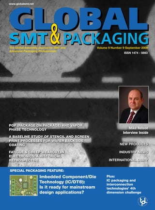
- 1. www.globalsmt.net The Global Assembly Journal for SMT and Volume 9 Number 9 September 2009 Advanced Packaging Professionals ISSN 1474 - 0893 PoP (Package on Package) and vaPor Phase technology Mike Nelson Interview Inside a baseline study of stencil and screen Print Processes for wafer backside coating NEW PRODUCTS fatigue & creeP wearout in INDUSTRY NEWS electronics: a historical retrosPective INTERNATIONAL DIARY sPecial Packaging feature: imbedded component/die Plus: ic packaging and technology (ic/dt®): interconnection is it ready for mainstream technologies’ 4th design applications? dimension challenge
- 2. PoP (package on package) and vapor phase technology PoP (package on package) and vapor phase technology by Dan Coada, EPIC Technologies LLC, Norwalk, Ohio, USA Increased use of PoP technology is driven technology are not significantly different The trend toward smaller, by continued product miniaturization. from individual BGAs. Following screen more densely populated Smaller products require increased printed printing, the first component is placed. electronic assemblies is circuit board assembly (PCBA) density. Then the second component is flux dipped driving increased use of Stacking memory is one way to achieve and placed. In some cases, up to two or both goals for enhanced functionality and more BGAs may be stacked. The only package-on-package (PoP) greater packaging density. significant line modification is purchasing technology ,and electronics PoP technology is not without manufac- a flux dip module for placement machines. manufacturing services (EMS) turing challenges. While the ball grid array Thermal profiling during reflow is the providers are developing viable (BGA) packages used are well understood, same as boards of similar thermal mass. manufacturing solutions. a poor quality process carries a far higher Quality needs to be carefully moni- cost in terms of rework or scrap, since two tored. Any distortion in the bottom com- or more BGAs are affected. ponent will be reflected in the components Placement requirements and process above it. Keywords: Package on Package, PoP, Vapor Phase Reflow, Solder Joint Formation Figure 1. A 2-D x-ray image of primary and secondary stacked BGAs pre-reflow indicated excellent placement accuracy. 10 – Global SMT & Packaging – September 2009 www.globalsmt.net
- 3. PoP (package on package) and vapor phase technology ! Excessive heat in convection reflow processes when lead-free components are used can be a concern because the top component is flux dipped; there is no addi- tional solder volume. The use of VP reflow is the only one that actually helps PoP technology by controlled peak temperature, no ΔT, and SVP (soft vapor phase) technol- ogy that gives an accurate control on ramp rates and reflow time. VP reflow technology is not a new process to the EMS industry. It is simply an alternative process for SMT reflow that has been in existence since the early 1970’s. Today’s VP reflow process makes use of the heat produced by an environ- mentally friendly boiling fluorinated fluid. !"!#$%&'#()*%# The vapor blanket is a uniform tempera- ture zone in which the PCBA solder is reflowed. Heat is transferred to the PCBA through condensation as it is immersed into the vapor area until the PCBA reaches temperature equilibrium with the boiling point of the fluid. The primary soldering benefits of VP, !"!#+%,'%-# in comparison to infrared (IR) or convec- tion, include an oxygen-free (inert) environ- ment without the need for nitrogen, fixed highest temperature exposure, and superior heat transfer on thermally challenging PCBAs. Vapor phase reflow offers two main advantages for PoP assembly: !"!#.)/0'#1)*%# • Better thermal transfer, which reduces the potential of “potato Figure 2. A micro-section image showed excellent ball collapse on primary and secondary packages after reflow. chipping” or cracking of the components that can occur if the proper thermal mass temperature is not achieved. • Reduced cost by avoiding a ni- trogen requirement for reflow. In our Reliability Laboratory at EPIC, we performed analysis on PoP assemblies reflowed using VP technology. The aim was to verify that solder joint formation between PoP BGAs and the PoP assembly and board pads conformed to IPC stan- dards. The test vehicle used a BGA305 and BGA128 assembly on a PCB200-12mmcad Practical Components testing board. Kester Tacky Flux RF743 was used for the flux dip operation and Henkel no-clean lead-free Multicore LF318 DAP88.5 for the solder paste. Five PoP BGA sets were placed and reflowed at 240˚C. Electrical testing, x-ray and cross sectioning were used to assess solder joint quality. In vapor phase reflow, heat is trans- ferred when the hot, saturated vapor condenses on the PCBA surface and gives up its latent heat of vaporization. The fluid boiling point is the governing factor in Figure 3. A darkened image of micro-section indicated excellent solderability, wetting, and ball collapse on peak temperature. The vapor encapsulates primary and secondary BGAs. Shown under a stereo (top) and metallurgical (bottom) microscope. the entire surface of the board, resulting in 12 – Global SMT & Packaging – September 2009 www.globalsmt.net
- 4. PoP (package on package) and vapor phase technology the smallest ΔT at short dwell times of the As a surface board in the condensing vapor. Thermal finish, ENIG transfer is independent of form, color, offered good solder- mass and mass distribution of the PCBA. ability, increasingly Detailed x-ray inspections were significant strength performed on each BGA group, looking and a considerably for evidence of solder bridges, voids and improved board Affordable, intelligently designed x-ray open connections. Voids were measured finish. using RINCON measuring software and Visual inspec- inspection systems since 1983. found compliant with IPC-7095 where tion under 40, 150, the accepted voiding area is less than 25% 600 and 1200X Patented real-time x-ray imaging (the percentage of joint cross-sectional area magnifications re- technology that creates high resolution, occupied by the void). Voiding was mainly sulted in 100% first compact systems. caused by flux out-gassing within molten pass yield (FPY) for solder joints. (These bubbles form and pop all BGAs that used open when they either grow too large or Multicore LF318M migrate to the edge of a joint; upon solidi- DAP solder paste fication, the bubbles become voids.) While under VP reflow. cross-sectioning was not perfectly centered All five BGAs on the BGA balls, the solder joints exhib- (U1, U5, U8, U11, ited in the analysis met all requirements and U15) were suc- of IPC-610 Revision D for component cessfully tested for alignment, voiding, solder ball spacing and continuity. connection (Figure 1). All criteria for Cross sections of the components that this process were used Multicore LF318M DAP solder paste satisfied with excel- together with VP reflow indicate adequate lent test results. solder volume and uniformity (Figures 2 and 3). The calculated solder volume used is within 5% of the solder volume that should normally occur on a production surface mount line. To learn more, go to: www.GlenbrookTech.com references: 1. Munroe, C., “Beating the RoHS Heat,” Circuits Assembly, March 2008. 2. Wooten, R., “Vapor Phase vs. Convection Re- flow Technology” SMT, July 2009 Dan Coada is a process/ manufacturing engineer with EPIC Technologies. He can be reached at coaddc@ epictech.com. Figure 4. Vapor Phase profile that has been used to reflow the boards. www.globalsmt.net Global SMT & Packaging – September 2009 – 13