SlideShare una empresa de Scribd logo
1 de 11
LOGIC GATES
module logic_gates(a,b,y1,y2,y3,y4,y5,y6,y7,y8);
   input a,b;
   output y1,y2,y3,y4,y5,y6,y7,y8;
    buf (y1,a);
   not (y2,a);
   or (y3,a,b);
   nor (y4,a,b);
   and (y5,a,b);
   nand (y6,a,b);
   xor (y7,a,b);
   xnor (y8,a,b);
endmodule


HALF ADDER & FULL ADDER
module half_adder(a,b,sum,carry);
  input a,b;
  output sum,carry;
   xor (sum,a,b);
   and (carry,a,b);
endmodule

module full_adder(a,b,c,sum,carry);
  input a,b,c;
  output sum,carry;
  assign sum = a^b^c;
  assign carry = (a&b)|(b&c)|(c&a);
endmodule


HALF SUBTRACTOR & FULL SUBTRACTOR
module half_subtractor (x,y,difference,borrow);
input x,y;
output difference,borrow ;
assign difference = (x^y),
        borrow =(~x&y);
endmodule

module full_subtractor (x,y,bin,d,bout);
input x,y,bin;
output d,bout;
assign d = (x^y^bin),
        bout =(~x&y)|(~x&bin)|(y&bin);
endmodule
PARALLEL ADDER
module parallel_adder(a,b,cin,sum,cout);
input [3:0] a,b;
input cin;
output [3:0] sum;
output cout;
assign {cout,sum}= a + b + cin;
endmodule

PARALLEL SUBTRACTOR
module parallel_subtractor(x,y,bin,difference,bout);
input [3:0] x,y;
input bin;
output [3:0] difference;
output bout;
assign {bout,difference}= x - y - bin;
endmodule

CARRY LOOK AHEAD ADDER
module CLA_adder (a,b,cin,sum,cout);
input [3:0]a,b;
input cin;
output[3:0]sum;
output cout;
wire po,p1,p2,p3,g0,g1,g2,g3;
wire c1,c2,c3,c4;
assign p0 = (a[0] ^ b[0]),
        p1 = (a[1] ^ b[1]),
        p2 = (a[2] ^ b[2]),
        p3 = (a[3] ^ b[3]);
assign g0 = (a[0] & b[0]),
        g1 = (a[1] & b[1]),
        g2 = (a[2] & b[2]),
        g3 = (a[3] & b[3]);
assign c0=cin,
       c1=g0 | (p0 & cin),
       c2 = g1 | (p0 & g0) | (p1 & p0 & cin),
       c3 = g2 | (p2 & g1) | (p2 & p1 & g0) | (p2 & p1 & p0 & cin),
       c4 = g3 | (p3 & g2) | (p3 & p2 & g1) | (p3 & p2 & p1 & g0) | (p3 & p2 & p1 & p0
& cin);
assign sum[0]=p0 ^ c0,
        sum[1]=p1 ^ c1,
        sum[2]=p2 ^ c2,
         sum[3]=p3 ^ c3;
assign cout = c4;
endmodule
PARALLEL ADDER & SUBTRACTOR
module parallel_add_sub( a3,a2,a1,a0,b3,b2,b1,b0,m,sum3,sum2,sum1,sum0,cout);
input a3,a2,a1,a0;
input b3,b2,b1,b0;
input m;
output sum3,sum2,sum1,sum0;
output cout;
wire cin,c0,c1,c2,d0,d1,d2,d3;
assign cin = m;
assign d0 = a0^m,
        d1=a1^m,
        d2=a2^m,
        d3=a3^m;
full_add ff0(b0,d0,cin,sum0,c0);
full_add ff1(b1,d1,c0,sum1,c1);
full_add ff2(b2,d2,c1,sum2,c2);
full_add ff3(b3,d3,c2,sum3,cout);
endmodule

module full_add(a,b,c,sum,carry);
  input a,b,c;
  output sum,carry;
  assign sum = a^b^c;
  assign carry = (a&b)|(b&c)|(c&a);
endmodule

8 :3 ENCODER & 3:8 DECODER
module encoder8_to_3(d0,d1,d2,d3,d4,d5,d6,d7,a,b,c);
   input d0,d1,d2,d3,d4,d5,d6,d7;
   output a,b,c;
   or (a,d4,d5,d6,d7);
   or(b,d2,d3,d6,d7);
   or (c,d1,d3,d5,d7);
endmodule

module decoder3_to_8(a,b,c,d0,d1,d2,d3,d4,d5,d6,d7);
   input a,b,c;
   output d0,d1,d2,d3,d4,d5,d6,d7 ;
   assign d0 = (~a & ~b&~c),
          d1 = (~a & ~b&c ),
          d2 = (~a & b&~c ),
          d3 = (~a & b&c ),
          d4 = (a & ~b&~c ),
          d5 = (a & ~b&c ),
          d6 = (a & b&~c ),
          d7 = (a &b&c );
endmodule
1 :8 DEMULTIPLEXER & 4:1 MULTIPLEXER

module demux1_to_8(i,s0,s1,s2,d0,d1,d2,d3,d4,d5,d6,d7);
      input i,s0,s1,s2;
      output d0,d1,d2,d3,d4,d5,d6,d7;
      assign d0 = (i & ~s2 & ~s1 & ~s0),
              d1 = (i & ~s2 & ~s1 & s0),
              d2 = (i & ~s2 & s1 & ~s0),
              d3 = (i & ~s2 & s1 & s0),
              d4 = (i & s2 & ~s1 & ~s0),
              d5 = (i & s2 & ~s1 & s0),
              d6 = (i & s2 & s1 & ~s0),
              d7 = (i & s2 & s1 & s0);
endmodule

module mux4_to_1(i0,i1,i2,i3,s0,s1,out);
      input i0,i1,i2,i3,s0,s1;
      output out;
      assign out = (i0 & ~s1 & ~s0)|(i1 & ~s1 & s0)|(i2 & s1 & ~s0)|(i3 & s1 & s0);
endmodule

8 BIT MULTIPLIER
module multiplier_8_bit (a,b,c);
      input [7:0]a;
      input [7:0]b;
      output [15:0]c;
      assign c[15:0] = a[7:0]*b[7:0];
endmodule

D FLIPFLOP
module D_FF (D,clk,reset,Q);
         input D,clk,reset;
         output Q;
         reg Q;
         always @ (posedge reset or negedge clk)
if (reset)
         Q = 1'b0;
else
         Q = D;
endmodule
T FLIPFLOP
module T_FF (T,clk,reset,Q);
      input T,clk,reset;
      output Q;
      wire w;
      assign w = T^Q;
      D_FF dff1(w,clk,reset,Q);
endmodule

module D_FF (D,clk,reset,Q);
         input D,clk,reset;
         output Q;
         reg Q;
         always @ (posedge reset or negedge clk)
if (reset)
         Q = 1'b0;
else
         Q = D;
endmodule


JK FLIPFLOP
module JK_FF (J,K,clk,reset,Q);
      input J,K,clk,reset;
      output Q;
      wire w;
      assign w = (J&~Q)|(~K&Q);
      D_FF dff1(w,clk,reset,Q);
endmodule

module D_FF (D,clk,reset,Q);
         input D,clk,reset;
         output Q;
         reg Q;
         always @ (posedge reset or negedge clk)
if (reset)
         Q = 1'b0;
else
         Q = D;
endmodule
SYNCHRONOUS UP-DOWN COUNTER
module updown_counter(up_down,clk,reset,count);
input [1:0]up_down;
input clk,reset;
output [2:0]count;
reg[2:0]count;
always @(posedge clk or posedge reset)
if (reset==1)count<=3'b000;
else
if(up_down==2'b00 ||up_down ==2'b11)
count<=count;
else
if(up_down==2'b01)
count<=count+1;
else
if(up_down==2'b10)
count<=count-1;
endmodule

UNIVERSAL SHIFT REGISTER
module unishft_reg(s1,s0,PIin,LFin,RTin,clk,reset,q3,q2,q1,q0);
input s1,s0;         // select inputs
input LFin,RTin;     // serial inputs
input clk,reset;
input[3:0]PIin;      // parallel input
output q3,q2,q1,q0; // register output
reg q3,q2,q1,q0;
always @ (posedge clk or posedge reset)
if (reset)
{q3,q2,q1,q0}=4'b0000;
else

case ({s1,s0})
        2'b00:{q3,q2,q1,q0}={q3,q2,q1,q0};         // No change
        2'b01:{q3,q2,q1,q0}={RTin,q3,q2,q1};       // Shift right
        2'b10:{q3,q2,q1,q0}={q2,q1,q0,LFin};       // Shift left
        2'b11:{q3,q2,q1,q0}=PIin;                  // Parallel load input
endcase
endmodule
CMOS INVERTER

module my_inv(in,out);
input in;
output out;
supply1 pwr;
supply0 gnd;
pmos ( out,pwr,in);
nmos (out,gnd,in);
endmodule

CMOS NOR GATE
module my_nor(a,b,out);
input a,b;
output out;
wire c;
supply1 pwr;
supply0 gnd;
pmos ( c,pwr,b);
pmos (out,c,a);
nmos(out,gnd,a);
nmos(out,gnd,b);
endmodule

CMOS NAND GATE
module my_nand(a,b,out);
input a,b;
output out;
wire c;
supply1 pwr;
supply0 gnd;
pmos ( out,pwr,a);
pmos (out,pwr,b);
nmos(out,c,a);
nmos(c,gnd,b);
endmodule
SR FLIPFLOP

module sr_flipflop(s,r,clk,q,qbar);
input s,r,clk;
output q,qbar;
reg q,qbar;
always@(posedge clk)
begin
   case ({s,r})
         2'b00:q=q;
         2'b01:q=1'b0;
         2'b10:q=1'b1;
         2'b11:q=1'bx;
   endcase
         qbar=~q;
 end
 endmodule


CMOS XOR GATE
module my_xor(a,b,out);
input a,b;
output out;
wire e,f,g;
supply1 pwr;
supply0 gnd;
assign c=~a;
assign d=~b;
pmos (e,pwr,c);
pmos (e,pwr,d);
pmos (out,e,a);
pmos (out,e,b);
nmos(out,f,a);
nmos(f,gnd,b);
nmos(out,g,c);
nmos(g,gnd,d);
endmodule
SERIAL ADDER

module serial_adder(count2,count1,count0,clk,a0,a1,a2,a3,a4,a5,a6,a7,a8,result,add);
input count2,count1,count0;
input clk;
input a0,a1,a2,a3,a4,a5,a6,a7,a8;
output [3:0]add ,result;
reg [3:0]result,add;
always @ (posedge clk )
case ({count2,count1,count0})

3'b000 :begin
add=a0+a1;
end

3'b001 :begin
add=add+a2;
end

3'b010 :begin
add=add+a3;
end

3'b011 :begin
add=add+a4;
end

3'b100 :begin
add=add+a5;
end

3'b101 :begin
add=add+a6;
end

3'b110 :begin
add=add+a7;
end

3'b111 :begin
result=add+a8;
end

endcase

endmodule
TRAFFIC LIGHT CONTROLLER

module tlc(state2,state1,state0,clk,r0,y0,g0,p0,r1,y1,g1,p1);
input state2,state1,state0;
input clk;
output r0,y0,g0,p0,r1,y1,g1,p1 ;
reg r0,y0,g0,p0,r1,y1,g1,p1;
always @ (posedge clk )
case ({state2,state1,state0})

3'b000 :begin
r0=1;
y0=0;
g0=0;
p0=1;
r1=1;
y1=0;
g1=0;
p1=1;
end

3'b001 :begin
r0=0;
y0=1;
g0=0;
p0=1;
r1=1;
y1=0;
g1=0;
p1=1;
end

3'b010 :begin
r0=0;
y0=0;
g0=1;
p0=0;
r1=1;
y1=0;
g1=0;
p1=0;
end
3'b011 :begin
r0=0;
y0=1;
g0=0;
p0=0;
r1=0;
y1=1;
g1=0;
p1=0;
end

3'b100 :begin
r0=1;
y0=0;
g0=0;
p0=0;
r1=0;
y1=0;
g1=1;
p1=0;
end

3'b101 :begin
r0=1;
y0=0;
g0=0;
p0=0;
r1=0;
y1=1;
g1=0;
p1=0;
end

default :begin
r0=0;
y0=0;
g0=0;
p0=0;
r1=0;
y1=0;
g1=0;
p1=0;
end

endcase
endmodule

Más contenido relacionado

La actualidad más candente

Verilog Tutorial - Verilog HDL Tutorial with Examples
Verilog Tutorial - Verilog HDL Tutorial with ExamplesVerilog Tutorial - Verilog HDL Tutorial with Examples
Verilog Tutorial - Verilog HDL Tutorial with ExamplesE2MATRIX
 
Lecture 2 verilog
Lecture 2   verilogLecture 2   verilog
Lecture 2 verilogvenravi10
 
Verilog full adder in dataflow & gate level modelling style.
Verilog full adder in dataflow  & gate level modelling style.Verilog full adder in dataflow  & gate level modelling style.
Verilog full adder in dataflow & gate level modelling style.Omkar Rane
 
VERILOG HDL :: Blocking & NON- Blocking assignments
VERILOG HDL :: Blocking & NON- Blocking assignments VERILOG HDL :: Blocking & NON- Blocking assignments
VERILOG HDL :: Blocking & NON- Blocking assignments Dr.YNM
 
Delays in verilog
Delays in verilogDelays in verilog
Delays in verilogJITU MISTRY
 
Programmable Peripheral Interface 8255
 Programmable Peripheral Interface   8255 Programmable Peripheral Interface   8255
Programmable Peripheral Interface 8255Dr.P.Parandaman
 
Introduction to FPGA, VHDL
Introduction to FPGA, VHDL  Introduction to FPGA, VHDL
Introduction to FPGA, VHDL Amr Rashed
 
Verilog Test Bench
Verilog Test BenchVerilog Test Bench
Verilog Test BenchDr.YNM
 
VHDL- gate level modelling
VHDL- gate level modellingVHDL- gate level modelling
VHDL- gate level modellingVandanaPagar1
 
Gate level design -For beginners
Gate level design -For beginnersGate level design -For beginners
Gate level design -For beginnersDr.YNM
 
Verilog presentation final
Verilog presentation finalVerilog presentation final
Verilog presentation finalAnkur Gupta
 
Timing Diagram of MVI Instruction of 8085 Microprocessor
Timing Diagram of MVI Instruction of 8085 MicroprocessorTiming Diagram of MVI Instruction of 8085 Microprocessor
Timing Diagram of MVI Instruction of 8085 MicroprocessorDhrumil Panchal
 
Verilog coding of mux 8 x1
Verilog coding of mux  8 x1Verilog coding of mux  8 x1
Verilog coding of mux 8 x1Rakesh kumar jha
 
VLSI Lab manual PDF
VLSI Lab manual PDFVLSI Lab manual PDF
VLSI Lab manual PDFUR11EC098
 
Verilog 語法教學
Verilog 語法教學 Verilog 語法教學
Verilog 語法教學 艾鍗科技
 

La actualidad más candente (20)

Verilog Tutorial - Verilog HDL Tutorial with Examples
Verilog Tutorial - Verilog HDL Tutorial with ExamplesVerilog Tutorial - Verilog HDL Tutorial with Examples
Verilog Tutorial - Verilog HDL Tutorial with Examples
 
Lecture 2 verilog
Lecture 2   verilogLecture 2   verilog
Lecture 2 verilog
 
Verilog full adder in dataflow & gate level modelling style.
Verilog full adder in dataflow  & gate level modelling style.Verilog full adder in dataflow  & gate level modelling style.
Verilog full adder in dataflow & gate level modelling style.
 
VERILOG HDL :: Blocking & NON- Blocking assignments
VERILOG HDL :: Blocking & NON- Blocking assignments VERILOG HDL :: Blocking & NON- Blocking assignments
VERILOG HDL :: Blocking & NON- Blocking assignments
 
Verilog tutorial
Verilog tutorialVerilog tutorial
Verilog tutorial
 
Delays in verilog
Delays in verilogDelays in verilog
Delays in verilog
 
Verilog hdl
Verilog hdlVerilog hdl
Verilog hdl
 
Programmable Peripheral Interface 8255
 Programmable Peripheral Interface   8255 Programmable Peripheral Interface   8255
Programmable Peripheral Interface 8255
 
Introduction to FPGA, VHDL
Introduction to FPGA, VHDL  Introduction to FPGA, VHDL
Introduction to FPGA, VHDL
 
Verilog Test Bench
Verilog Test BenchVerilog Test Bench
Verilog Test Bench
 
VHDL- gate level modelling
VHDL- gate level modellingVHDL- gate level modelling
VHDL- gate level modelling
 
Gate level design -For beginners
Gate level design -For beginnersGate level design -For beginners
Gate level design -For beginners
 
Verilog presentation final
Verilog presentation finalVerilog presentation final
Verilog presentation final
 
Timing Diagram of MVI Instruction of 8085 Microprocessor
Timing Diagram of MVI Instruction of 8085 MicroprocessorTiming Diagram of MVI Instruction of 8085 Microprocessor
Timing Diagram of MVI Instruction of 8085 Microprocessor
 
Verilog coding of mux 8 x1
Verilog coding of mux  8 x1Verilog coding of mux  8 x1
Verilog coding of mux 8 x1
 
Verilog
VerilogVerilog
Verilog
 
SPI Bus Protocol
SPI Bus ProtocolSPI Bus Protocol
SPI Bus Protocol
 
VLSI Lab manual PDF
VLSI Lab manual PDFVLSI Lab manual PDF
VLSI Lab manual PDF
 
verilog
verilogverilog
verilog
 
Verilog 語法教學
Verilog 語法教學 Verilog 語法教學
Verilog 語法教學
 

Destacado

Bit Serial multiplier using Verilog
Bit Serial multiplier using VerilogBit Serial multiplier using Verilog
Bit Serial multiplier using VerilogBhargavKatkam
 
The Multipliers Seminar
The Multipliers SeminarThe Multipliers Seminar
The Multipliers SeminarGreg McKeown
 
DESIGN AND SIMULATION OF DIFFERENT 8-BIT MULTIPLIERS USING VERILOG CODE BY SA...
DESIGN AND SIMULATION OF DIFFERENT 8-BIT MULTIPLIERS USING VERILOG CODE BY SA...DESIGN AND SIMULATION OF DIFFERENT 8-BIT MULTIPLIERS USING VERILOG CODE BY SA...
DESIGN AND SIMULATION OF DIFFERENT 8-BIT MULTIPLIERS USING VERILOG CODE BY SA...Saikiran Panjala
 

Destacado (9)

Bit Serial multiplier using Verilog
Bit Serial multiplier using VerilogBit Serial multiplier using Verilog
Bit Serial multiplier using Verilog
 
Mux based array mul ppt
Mux based array mul pptMux based array mul ppt
Mux based array mul ppt
 
Multipliers in VLSI
Multipliers in VLSIMultipliers in VLSI
Multipliers in VLSI
 
The Multipliers Seminar
The Multipliers SeminarThe Multipliers Seminar
The Multipliers Seminar
 
VERILOG CODE
VERILOG CODEVERILOG CODE
VERILOG CODE
 
DESIGN AND SIMULATION OF DIFFERENT 8-BIT MULTIPLIERS USING VERILOG CODE BY SA...
DESIGN AND SIMULATION OF DIFFERENT 8-BIT MULTIPLIERS USING VERILOG CODE BY SA...DESIGN AND SIMULATION OF DIFFERENT 8-BIT MULTIPLIERS USING VERILOG CODE BY SA...
DESIGN AND SIMULATION OF DIFFERENT 8-BIT MULTIPLIERS USING VERILOG CODE BY SA...
 
Array multiplier
Array multiplierArray multiplier
Array multiplier
 
Programs of VHDL
Programs of VHDLPrograms of VHDL
Programs of VHDL
 
Booth Multiplier
Booth MultiplierBooth Multiplier
Booth Multiplier
 

Similar a All VLSI programs

VLSI experiments II
VLSI experiments IIVLSI experiments II
VLSI experiments IIGouthaman V
 
Combinational circuits II outputs
Combinational circuits II outputsCombinational circuits II outputs
Combinational circuits II outputsGouthaman V
 
Graphics programs
Graphics programsGraphics programs
Graphics programsNAVYA RAO
 
Digital System Design-Synchronous Sequential Circuits
Digital System Design-Synchronous Sequential CircuitsDigital System Design-Synchronous Sequential Circuits
Digital System Design-Synchronous Sequential CircuitsIndira Priyadarshini
 
Sequential Circuits I VLSI 9th experiment
Sequential Circuits I VLSI 9th experimentSequential Circuits I VLSI 9th experiment
Sequential Circuits I VLSI 9th experimentGouthaman V
 
Paradigmas de Linguagens de Programacao - Aula #4
Paradigmas de Linguagens de Programacao - Aula #4Paradigmas de Linguagens de Programacao - Aula #4
Paradigmas de Linguagens de Programacao - Aula #4Ismar Silveira
 
Verilog code all
Verilog code allVerilog code all
Verilog code allMNIT jaipur
 
SICP勉強会について
SICP勉強会についてSICP勉強会について
SICP勉強会についてYusuke Sasaki
 
Как работает LLVM бэкенд в C#. Егор Богатов ➠ CoreHard Autumn 2019
Как работает LLVM бэкенд в C#. Егор Богатов ➠ CoreHard Autumn 2019Как работает LLVM бэкенд в C#. Егор Богатов ➠ CoreHard Autumn 2019
Как работает LLVM бэкенд в C#. Егор Богатов ➠ CoreHard Autumn 2019corehard_by
 
C programs Set 2
C programs Set 2C programs Set 2
C programs Set 2Koshy Geoji
 
HDL PROGRAMMING-3.pdf
HDL PROGRAMMING-3.pdfHDL PROGRAMMING-3.pdf
HDL PROGRAMMING-3.pdfkaarthikK6
 
Verilog programs for basic logic gates
Verilog programs for basic logic gatesVerilog programs for basic logic gates
Verilog programs for basic logic gatesSriSudharsnaRathinas
 
TOC(CS-501) (19-49).pdf
TOC(CS-501) (19-49).pdfTOC(CS-501) (19-49).pdf
TOC(CS-501) (19-49).pdfRajJain516913
 
Day4 順序控制的循序邏輯實現
Day4 順序控制的循序邏輯實現Day4 順序控制的循序邏輯實現
Day4 順序控制的循序邏輯實現Ron Liu
 
Computer graphics lab assignment
Computer graphics lab assignmentComputer graphics lab assignment
Computer graphics lab assignmentAbdullah Al Shiam
 

Similar a All VLSI programs (20)

VLSI experiments II
VLSI experiments IIVLSI experiments II
VLSI experiments II
 
Task i
Task iTask i
Task i
 
Combinational circuits II outputs
Combinational circuits II outputsCombinational circuits II outputs
Combinational circuits II outputs
 
mod-4.pptx
mod-4.pptxmod-4.pptx
mod-4.pptx
 
Graphics programs
Graphics programsGraphics programs
Graphics programs
 
Digital System Design-Synchronous Sequential Circuits
Digital System Design-Synchronous Sequential CircuitsDigital System Design-Synchronous Sequential Circuits
Digital System Design-Synchronous Sequential Circuits
 
Sequential Circuits I VLSI 9th experiment
Sequential Circuits I VLSI 9th experimentSequential Circuits I VLSI 9th experiment
Sequential Circuits I VLSI 9th experiment
 
VerilogHDL_Utkarsh_kulshrestha
VerilogHDL_Utkarsh_kulshresthaVerilogHDL_Utkarsh_kulshrestha
VerilogHDL_Utkarsh_kulshrestha
 
Paradigmas de Linguagens de Programacao - Aula #4
Paradigmas de Linguagens de Programacao - Aula #4Paradigmas de Linguagens de Programacao - Aula #4
Paradigmas de Linguagens de Programacao - Aula #4
 
Verilog code all
Verilog code allVerilog code all
Verilog code all
 
SICP勉強会について
SICP勉強会についてSICP勉強会について
SICP勉強会について
 
Как работает LLVM бэкенд в C#. Егор Богатов ➠ CoreHard Autumn 2019
Как работает LLVM бэкенд в C#. Егор Богатов ➠ CoreHard Autumn 2019Как работает LLVM бэкенд в C#. Егор Богатов ➠ CoreHard Autumn 2019
Как работает LLVM бэкенд в C#. Егор Богатов ➠ CoreHard Autumn 2019
 
C programs Set 2
C programs Set 2C programs Set 2
C programs Set 2
 
PRACTICAL COMPUTING
PRACTICAL COMPUTINGPRACTICAL COMPUTING
PRACTICAL COMPUTING
 
HDL PROGRAMMING-3.pdf
HDL PROGRAMMING-3.pdfHDL PROGRAMMING-3.pdf
HDL PROGRAMMING-3.pdf
 
Verilog programs for basic logic gates
Verilog programs for basic logic gatesVerilog programs for basic logic gates
Verilog programs for basic logic gates
 
TOC(CS-501) (19-49).pdf
TOC(CS-501) (19-49).pdfTOC(CS-501) (19-49).pdf
TOC(CS-501) (19-49).pdf
 
Vcs9
Vcs9Vcs9
Vcs9
 
Day4 順序控制的循序邏輯實現
Day4 順序控制的循序邏輯實現Day4 順序控制的循序邏輯實現
Day4 順序控制的循序邏輯實現
 
Computer graphics lab assignment
Computer graphics lab assignmentComputer graphics lab assignment
Computer graphics lab assignment
 

Más de Gouthaman V

Professional Ethics Assignment II
Professional Ethics Assignment IIProfessional Ethics Assignment II
Professional Ethics Assignment IIGouthaman V
 
Scholastic averages sheet-2
Scholastic averages sheet-2Scholastic averages sheet-2
Scholastic averages sheet-2Gouthaman V
 
Eligibility criteria and instructions for Infosys Placement
Eligibility criteria and instructions for Infosys PlacementEligibility criteria and instructions for Infosys Placement
Eligibility criteria and instructions for Infosys PlacementGouthaman V
 
Answers for 2 Marks Unit Test I (RMW)
Answers for 2 Marks Unit Test I (RMW)Answers for 2 Marks Unit Test I (RMW)
Answers for 2 Marks Unit Test I (RMW)Gouthaman V
 
Anwers for 2 marks - RMW
Anwers for 2 marks - RMWAnwers for 2 marks - RMW
Anwers for 2 marks - RMWGouthaman V
 
Rmw unit test question papers
Rmw unit test question papersRmw unit test question papers
Rmw unit test question papersGouthaman V
 
Circular and semicircular cavity resonator
Circular and semicircular cavity resonatorCircular and semicircular cavity resonator
Circular and semicircular cavity resonatorGouthaman V
 
VLSI Anna University Practical Examination
VLSI Anna University Practical ExaminationVLSI Anna University Practical Examination
VLSI Anna University Practical ExaminationGouthaman V
 
VLSI Sequential Circuits II
VLSI Sequential Circuits IIVLSI Sequential Circuits II
VLSI Sequential Circuits IIGouthaman V
 
VI Semester Examination Time Table
VI Semester Examination Time TableVI Semester Examination Time Table
VI Semester Examination Time TableGouthaman V
 
Antenna and Wave Propagation Assignment I
Antenna and Wave Propagation Assignment IAntenna and Wave Propagation Assignment I
Antenna and Wave Propagation Assignment IGouthaman V
 
Antenna and Wave Propagation Assignment I
Antenna and Wave Propagation Assignment IAntenna and Wave Propagation Assignment I
Antenna and Wave Propagation Assignment IGouthaman V
 
Computer Networks Unit Test II Questions
Computer Networks Unit Test II QuestionsComputer Networks Unit Test II Questions
Computer Networks Unit Test II QuestionsGouthaman V
 
Antenna Unit Test II Questions
Antenna Unit Test II QuestionsAntenna Unit Test II Questions
Antenna Unit Test II QuestionsGouthaman V
 
Antenna Unit Test II questions
Antenna Unit Test II questionsAntenna Unit Test II questions
Antenna Unit Test II questionsGouthaman V
 
POM Unit Test II - ECE B
POM Unit Test II - ECE BPOM Unit Test II - ECE B
POM Unit Test II - ECE BGouthaman V
 
VLSI Experiments I
VLSI Experiments IVLSI Experiments I
VLSI Experiments IGouthaman V
 

Más de Gouthaman V (20)

Professional Ethics Assignment II
Professional Ethics Assignment IIProfessional Ethics Assignment II
Professional Ethics Assignment II
 
Dip Unit Test-I
Dip Unit Test-IDip Unit Test-I
Dip Unit Test-I
 
Scholastic averages sheet-2
Scholastic averages sheet-2Scholastic averages sheet-2
Scholastic averages sheet-2
 
Eligibility criteria and instructions for Infosys Placement
Eligibility criteria and instructions for Infosys PlacementEligibility criteria and instructions for Infosys Placement
Eligibility criteria and instructions for Infosys Placement
 
Answers for 2 Marks Unit Test I (RMW)
Answers for 2 Marks Unit Test I (RMW)Answers for 2 Marks Unit Test I (RMW)
Answers for 2 Marks Unit Test I (RMW)
 
Anwers for 2 marks - RMW
Anwers for 2 marks - RMWAnwers for 2 marks - RMW
Anwers for 2 marks - RMW
 
Rmw unit test question papers
Rmw unit test question papersRmw unit test question papers
Rmw unit test question papers
 
Circular and semicircular cavity resonator
Circular and semicircular cavity resonatorCircular and semicircular cavity resonator
Circular and semicircular cavity resonator
 
VLSI Anna University Practical Examination
VLSI Anna University Practical ExaminationVLSI Anna University Practical Examination
VLSI Anna University Practical Examination
 
HCL IPT
HCL IPTHCL IPT
HCL IPT
 
VLSI Sequential Circuits II
VLSI Sequential Circuits IIVLSI Sequential Circuits II
VLSI Sequential Circuits II
 
VI Semester Examination Time Table
VI Semester Examination Time TableVI Semester Examination Time Table
VI Semester Examination Time Table
 
Email
EmailEmail
Email
 
Antenna and Wave Propagation Assignment I
Antenna and Wave Propagation Assignment IAntenna and Wave Propagation Assignment I
Antenna and Wave Propagation Assignment I
 
Antenna and Wave Propagation Assignment I
Antenna and Wave Propagation Assignment IAntenna and Wave Propagation Assignment I
Antenna and Wave Propagation Assignment I
 
Computer Networks Unit Test II Questions
Computer Networks Unit Test II QuestionsComputer Networks Unit Test II Questions
Computer Networks Unit Test II Questions
 
Antenna Unit Test II Questions
Antenna Unit Test II QuestionsAntenna Unit Test II Questions
Antenna Unit Test II Questions
 
Antenna Unit Test II questions
Antenna Unit Test II questionsAntenna Unit Test II questions
Antenna Unit Test II questions
 
POM Unit Test II - ECE B
POM Unit Test II - ECE BPOM Unit Test II - ECE B
POM Unit Test II - ECE B
 
VLSI Experiments I
VLSI Experiments IVLSI Experiments I
VLSI Experiments I
 

Último

Marketplace and Quality Assurance Presentation - Vincent Chirchir
Marketplace and Quality Assurance Presentation - Vincent ChirchirMarketplace and Quality Assurance Presentation - Vincent Chirchir
Marketplace and Quality Assurance Presentation - Vincent Chirchirictsugar
 
TriStar Gold Corporate Presentation - April 2024
TriStar Gold Corporate Presentation - April 2024TriStar Gold Corporate Presentation - April 2024
TriStar Gold Corporate Presentation - April 2024Adnet Communications
 
Unlocking the Future: Explore Web 3.0 Workshop to Start Earning Today!
Unlocking the Future: Explore Web 3.0 Workshop to Start Earning Today!Unlocking the Future: Explore Web 3.0 Workshop to Start Earning Today!
Unlocking the Future: Explore Web 3.0 Workshop to Start Earning Today!Doge Mining Website
 
Cybersecurity Awareness Training Presentation v2024.03
Cybersecurity Awareness Training Presentation v2024.03Cybersecurity Awareness Training Presentation v2024.03
Cybersecurity Awareness Training Presentation v2024.03DallasHaselhorst
 
International Business Environments and Operations 16th Global Edition test b...
International Business Environments and Operations 16th Global Edition test b...International Business Environments and Operations 16th Global Edition test b...
International Business Environments and Operations 16th Global Edition test b...ssuserf63bd7
 
8447779800, Low rate Call girls in Kotla Mubarakpur Delhi NCR
8447779800, Low rate Call girls in Kotla Mubarakpur Delhi NCR8447779800, Low rate Call girls in Kotla Mubarakpur Delhi NCR
8447779800, Low rate Call girls in Kotla Mubarakpur Delhi NCRashishs7044
 
Darshan Hiranandani [News About Next CEO].pdf
Darshan Hiranandani [News About Next CEO].pdfDarshan Hiranandani [News About Next CEO].pdf
Darshan Hiranandani [News About Next CEO].pdfShashank Mehta
 
Youth Involvement in an Innovative Coconut Value Chain by Mwalimu Menza
Youth Involvement in an Innovative Coconut Value Chain by Mwalimu MenzaYouth Involvement in an Innovative Coconut Value Chain by Mwalimu Menza
Youth Involvement in an Innovative Coconut Value Chain by Mwalimu Menzaictsugar
 
Memorándum de Entendimiento (MoU) entre Codelco y SQM
Memorándum de Entendimiento (MoU) entre Codelco y SQMMemorándum de Entendimiento (MoU) entre Codelco y SQM
Memorándum de Entendimiento (MoU) entre Codelco y SQMVoces Mineras
 
Innovation Conference 5th March 2024.pdf
Innovation Conference 5th March 2024.pdfInnovation Conference 5th March 2024.pdf
Innovation Conference 5th March 2024.pdfrichard876048
 
8447779800, Low rate Call girls in Uttam Nagar Delhi NCR
8447779800, Low rate Call girls in Uttam Nagar Delhi NCR8447779800, Low rate Call girls in Uttam Nagar Delhi NCR
8447779800, Low rate Call girls in Uttam Nagar Delhi NCRashishs7044
 
8447779800, Low rate Call girls in Saket Delhi NCR
8447779800, Low rate Call girls in Saket Delhi NCR8447779800, Low rate Call girls in Saket Delhi NCR
8447779800, Low rate Call girls in Saket Delhi NCRashishs7044
 
Independent Call Girls Andheri Nightlaila 9967584737
Independent Call Girls Andheri Nightlaila 9967584737Independent Call Girls Andheri Nightlaila 9967584737
Independent Call Girls Andheri Nightlaila 9967584737Riya Pathan
 
Market Sizes Sample Report - 2024 Edition
Market Sizes Sample Report - 2024 EditionMarket Sizes Sample Report - 2024 Edition
Market Sizes Sample Report - 2024 EditionMintel Group
 
Ten Organizational Design Models to align structure and operations to busines...
Ten Organizational Design Models to align structure and operations to busines...Ten Organizational Design Models to align structure and operations to busines...
Ten Organizational Design Models to align structure and operations to busines...Seta Wicaksana
 
Church Building Grants To Assist With New Construction, Additions, And Restor...
Church Building Grants To Assist With New Construction, Additions, And Restor...Church Building Grants To Assist With New Construction, Additions, And Restor...
Church Building Grants To Assist With New Construction, Additions, And Restor...Americas Got Grants
 
Global Scenario On Sustainable and Resilient Coconut Industry by Dr. Jelfina...
Global Scenario On Sustainable  and Resilient Coconut Industry by Dr. Jelfina...Global Scenario On Sustainable  and Resilient Coconut Industry by Dr. Jelfina...
Global Scenario On Sustainable and Resilient Coconut Industry by Dr. Jelfina...ictsugar
 
Pitch Deck Teardown: Geodesic.Life's $500k Pre-seed deck
Pitch Deck Teardown: Geodesic.Life's $500k Pre-seed deckPitch Deck Teardown: Geodesic.Life's $500k Pre-seed deck
Pitch Deck Teardown: Geodesic.Life's $500k Pre-seed deckHajeJanKamps
 

Último (20)

Marketplace and Quality Assurance Presentation - Vincent Chirchir
Marketplace and Quality Assurance Presentation - Vincent ChirchirMarketplace and Quality Assurance Presentation - Vincent Chirchir
Marketplace and Quality Assurance Presentation - Vincent Chirchir
 
TriStar Gold Corporate Presentation - April 2024
TriStar Gold Corporate Presentation - April 2024TriStar Gold Corporate Presentation - April 2024
TriStar Gold Corporate Presentation - April 2024
 
Unlocking the Future: Explore Web 3.0 Workshop to Start Earning Today!
Unlocking the Future: Explore Web 3.0 Workshop to Start Earning Today!Unlocking the Future: Explore Web 3.0 Workshop to Start Earning Today!
Unlocking the Future: Explore Web 3.0 Workshop to Start Earning Today!
 
Cybersecurity Awareness Training Presentation v2024.03
Cybersecurity Awareness Training Presentation v2024.03Cybersecurity Awareness Training Presentation v2024.03
Cybersecurity Awareness Training Presentation v2024.03
 
International Business Environments and Operations 16th Global Edition test b...
International Business Environments and Operations 16th Global Edition test b...International Business Environments and Operations 16th Global Edition test b...
International Business Environments and Operations 16th Global Edition test b...
 
Enjoy ➥8448380779▻ Call Girls In Sector 18 Noida Escorts Delhi NCR
Enjoy ➥8448380779▻ Call Girls In Sector 18 Noida Escorts Delhi NCREnjoy ➥8448380779▻ Call Girls In Sector 18 Noida Escorts Delhi NCR
Enjoy ➥8448380779▻ Call Girls In Sector 18 Noida Escorts Delhi NCR
 
8447779800, Low rate Call girls in Kotla Mubarakpur Delhi NCR
8447779800, Low rate Call girls in Kotla Mubarakpur Delhi NCR8447779800, Low rate Call girls in Kotla Mubarakpur Delhi NCR
8447779800, Low rate Call girls in Kotla Mubarakpur Delhi NCR
 
Darshan Hiranandani [News About Next CEO].pdf
Darshan Hiranandani [News About Next CEO].pdfDarshan Hiranandani [News About Next CEO].pdf
Darshan Hiranandani [News About Next CEO].pdf
 
Youth Involvement in an Innovative Coconut Value Chain by Mwalimu Menza
Youth Involvement in an Innovative Coconut Value Chain by Mwalimu MenzaYouth Involvement in an Innovative Coconut Value Chain by Mwalimu Menza
Youth Involvement in an Innovative Coconut Value Chain by Mwalimu Menza
 
Memorándum de Entendimiento (MoU) entre Codelco y SQM
Memorándum de Entendimiento (MoU) entre Codelco y SQMMemorándum de Entendimiento (MoU) entre Codelco y SQM
Memorándum de Entendimiento (MoU) entre Codelco y SQM
 
Innovation Conference 5th March 2024.pdf
Innovation Conference 5th March 2024.pdfInnovation Conference 5th March 2024.pdf
Innovation Conference 5th March 2024.pdf
 
8447779800, Low rate Call girls in Uttam Nagar Delhi NCR
8447779800, Low rate Call girls in Uttam Nagar Delhi NCR8447779800, Low rate Call girls in Uttam Nagar Delhi NCR
8447779800, Low rate Call girls in Uttam Nagar Delhi NCR
 
8447779800, Low rate Call girls in Saket Delhi NCR
8447779800, Low rate Call girls in Saket Delhi NCR8447779800, Low rate Call girls in Saket Delhi NCR
8447779800, Low rate Call girls in Saket Delhi NCR
 
Independent Call Girls Andheri Nightlaila 9967584737
Independent Call Girls Andheri Nightlaila 9967584737Independent Call Girls Andheri Nightlaila 9967584737
Independent Call Girls Andheri Nightlaila 9967584737
 
Corporate Profile 47Billion Information Technology
Corporate Profile 47Billion Information TechnologyCorporate Profile 47Billion Information Technology
Corporate Profile 47Billion Information Technology
 
Market Sizes Sample Report - 2024 Edition
Market Sizes Sample Report - 2024 EditionMarket Sizes Sample Report - 2024 Edition
Market Sizes Sample Report - 2024 Edition
 
Ten Organizational Design Models to align structure and operations to busines...
Ten Organizational Design Models to align structure and operations to busines...Ten Organizational Design Models to align structure and operations to busines...
Ten Organizational Design Models to align structure and operations to busines...
 
Church Building Grants To Assist With New Construction, Additions, And Restor...
Church Building Grants To Assist With New Construction, Additions, And Restor...Church Building Grants To Assist With New Construction, Additions, And Restor...
Church Building Grants To Assist With New Construction, Additions, And Restor...
 
Global Scenario On Sustainable and Resilient Coconut Industry by Dr. Jelfina...
Global Scenario On Sustainable  and Resilient Coconut Industry by Dr. Jelfina...Global Scenario On Sustainable  and Resilient Coconut Industry by Dr. Jelfina...
Global Scenario On Sustainable and Resilient Coconut Industry by Dr. Jelfina...
 
Pitch Deck Teardown: Geodesic.Life's $500k Pre-seed deck
Pitch Deck Teardown: Geodesic.Life's $500k Pre-seed deckPitch Deck Teardown: Geodesic.Life's $500k Pre-seed deck
Pitch Deck Teardown: Geodesic.Life's $500k Pre-seed deck
 

All VLSI programs

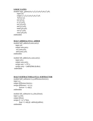
  • 1. LOGIC GATES module logic_gates(a,b,y1,y2,y3,y4,y5,y6,y7,y8); input a,b; output y1,y2,y3,y4,y5,y6,y7,y8; buf (y1,a); not (y2,a); or (y3,a,b); nor (y4,a,b); and (y5,a,b); nand (y6,a,b); xor (y7,a,b); xnor (y8,a,b); endmodule HALF ADDER & FULL ADDER module half_adder(a,b,sum,carry); input a,b; output sum,carry; xor (sum,a,b); and (carry,a,b); endmodule module full_adder(a,b,c,sum,carry); input a,b,c; output sum,carry; assign sum = a^b^c; assign carry = (a&b)|(b&c)|(c&a); endmodule HALF SUBTRACTOR & FULL SUBTRACTOR module half_subtractor (x,y,difference,borrow); input x,y; output difference,borrow ; assign difference = (x^y), borrow =(~x&y); endmodule module full_subtractor (x,y,bin,d,bout); input x,y,bin; output d,bout; assign d = (x^y^bin), bout =(~x&y)|(~x&bin)|(y&bin); endmodule
  • 2. PARALLEL ADDER module parallel_adder(a,b,cin,sum,cout); input [3:0] a,b; input cin; output [3:0] sum; output cout; assign {cout,sum}= a + b + cin; endmodule PARALLEL SUBTRACTOR module parallel_subtractor(x,y,bin,difference,bout); input [3:0] x,y; input bin; output [3:0] difference; output bout; assign {bout,difference}= x - y - bin; endmodule CARRY LOOK AHEAD ADDER module CLA_adder (a,b,cin,sum,cout); input [3:0]a,b; input cin; output[3:0]sum; output cout; wire po,p1,p2,p3,g0,g1,g2,g3; wire c1,c2,c3,c4; assign p0 = (a[0] ^ b[0]), p1 = (a[1] ^ b[1]), p2 = (a[2] ^ b[2]), p3 = (a[3] ^ b[3]); assign g0 = (a[0] & b[0]), g1 = (a[1] & b[1]), g2 = (a[2] & b[2]), g3 = (a[3] & b[3]); assign c0=cin, c1=g0 | (p0 & cin), c2 = g1 | (p0 & g0) | (p1 & p0 & cin), c3 = g2 | (p2 & g1) | (p2 & p1 & g0) | (p2 & p1 & p0 & cin), c4 = g3 | (p3 & g2) | (p3 & p2 & g1) | (p3 & p2 & p1 & g0) | (p3 & p2 & p1 & p0 & cin); assign sum[0]=p0 ^ c0, sum[1]=p1 ^ c1, sum[2]=p2 ^ c2, sum[3]=p3 ^ c3; assign cout = c4; endmodule
  • 3. PARALLEL ADDER & SUBTRACTOR module parallel_add_sub( a3,a2,a1,a0,b3,b2,b1,b0,m,sum3,sum2,sum1,sum0,cout); input a3,a2,a1,a0; input b3,b2,b1,b0; input m; output sum3,sum2,sum1,sum0; output cout; wire cin,c0,c1,c2,d0,d1,d2,d3; assign cin = m; assign d0 = a0^m, d1=a1^m, d2=a2^m, d3=a3^m; full_add ff0(b0,d0,cin,sum0,c0); full_add ff1(b1,d1,c0,sum1,c1); full_add ff2(b2,d2,c1,sum2,c2); full_add ff3(b3,d3,c2,sum3,cout); endmodule module full_add(a,b,c,sum,carry); input a,b,c; output sum,carry; assign sum = a^b^c; assign carry = (a&b)|(b&c)|(c&a); endmodule 8 :3 ENCODER & 3:8 DECODER module encoder8_to_3(d0,d1,d2,d3,d4,d5,d6,d7,a,b,c); input d0,d1,d2,d3,d4,d5,d6,d7; output a,b,c; or (a,d4,d5,d6,d7); or(b,d2,d3,d6,d7); or (c,d1,d3,d5,d7); endmodule module decoder3_to_8(a,b,c,d0,d1,d2,d3,d4,d5,d6,d7); input a,b,c; output d0,d1,d2,d3,d4,d5,d6,d7 ; assign d0 = (~a & ~b&~c), d1 = (~a & ~b&c ), d2 = (~a & b&~c ), d3 = (~a & b&c ), d4 = (a & ~b&~c ), d5 = (a & ~b&c ), d6 = (a & b&~c ), d7 = (a &b&c ); endmodule
  • 4. 1 :8 DEMULTIPLEXER & 4:1 MULTIPLEXER module demux1_to_8(i,s0,s1,s2,d0,d1,d2,d3,d4,d5,d6,d7); input i,s0,s1,s2; output d0,d1,d2,d3,d4,d5,d6,d7; assign d0 = (i & ~s2 & ~s1 & ~s0), d1 = (i & ~s2 & ~s1 & s0), d2 = (i & ~s2 & s1 & ~s0), d3 = (i & ~s2 & s1 & s0), d4 = (i & s2 & ~s1 & ~s0), d5 = (i & s2 & ~s1 & s0), d6 = (i & s2 & s1 & ~s0), d7 = (i & s2 & s1 & s0); endmodule module mux4_to_1(i0,i1,i2,i3,s0,s1,out); input i0,i1,i2,i3,s0,s1; output out; assign out = (i0 & ~s1 & ~s0)|(i1 & ~s1 & s0)|(i2 & s1 & ~s0)|(i3 & s1 & s0); endmodule 8 BIT MULTIPLIER module multiplier_8_bit (a,b,c); input [7:0]a; input [7:0]b; output [15:0]c; assign c[15:0] = a[7:0]*b[7:0]; endmodule D FLIPFLOP module D_FF (D,clk,reset,Q); input D,clk,reset; output Q; reg Q; always @ (posedge reset or negedge clk) if (reset) Q = 1'b0; else Q = D; endmodule
  • 5. T FLIPFLOP module T_FF (T,clk,reset,Q); input T,clk,reset; output Q; wire w; assign w = T^Q; D_FF dff1(w,clk,reset,Q); endmodule module D_FF (D,clk,reset,Q); input D,clk,reset; output Q; reg Q; always @ (posedge reset or negedge clk) if (reset) Q = 1'b0; else Q = D; endmodule JK FLIPFLOP module JK_FF (J,K,clk,reset,Q); input J,K,clk,reset; output Q; wire w; assign w = (J&~Q)|(~K&Q); D_FF dff1(w,clk,reset,Q); endmodule module D_FF (D,clk,reset,Q); input D,clk,reset; output Q; reg Q; always @ (posedge reset or negedge clk) if (reset) Q = 1'b0; else Q = D; endmodule
  • 6. SYNCHRONOUS UP-DOWN COUNTER module updown_counter(up_down,clk,reset,count); input [1:0]up_down; input clk,reset; output [2:0]count; reg[2:0]count; always @(posedge clk or posedge reset) if (reset==1)count<=3'b000; else if(up_down==2'b00 ||up_down ==2'b11) count<=count; else if(up_down==2'b01) count<=count+1; else if(up_down==2'b10) count<=count-1; endmodule UNIVERSAL SHIFT REGISTER module unishft_reg(s1,s0,PIin,LFin,RTin,clk,reset,q3,q2,q1,q0); input s1,s0; // select inputs input LFin,RTin; // serial inputs input clk,reset; input[3:0]PIin; // parallel input output q3,q2,q1,q0; // register output reg q3,q2,q1,q0; always @ (posedge clk or posedge reset) if (reset) {q3,q2,q1,q0}=4'b0000; else case ({s1,s0}) 2'b00:{q3,q2,q1,q0}={q3,q2,q1,q0}; // No change 2'b01:{q3,q2,q1,q0}={RTin,q3,q2,q1}; // Shift right 2'b10:{q3,q2,q1,q0}={q2,q1,q0,LFin}; // Shift left 2'b11:{q3,q2,q1,q0}=PIin; // Parallel load input endcase endmodule
  • 7. CMOS INVERTER module my_inv(in,out); input in; output out; supply1 pwr; supply0 gnd; pmos ( out,pwr,in); nmos (out,gnd,in); endmodule CMOS NOR GATE module my_nor(a,b,out); input a,b; output out; wire c; supply1 pwr; supply0 gnd; pmos ( c,pwr,b); pmos (out,c,a); nmos(out,gnd,a); nmos(out,gnd,b); endmodule CMOS NAND GATE module my_nand(a,b,out); input a,b; output out; wire c; supply1 pwr; supply0 gnd; pmos ( out,pwr,a); pmos (out,pwr,b); nmos(out,c,a); nmos(c,gnd,b); endmodule
  • 8. SR FLIPFLOP module sr_flipflop(s,r,clk,q,qbar); input s,r,clk; output q,qbar; reg q,qbar; always@(posedge clk) begin case ({s,r}) 2'b00:q=q; 2'b01:q=1'b0; 2'b10:q=1'b1; 2'b11:q=1'bx; endcase qbar=~q; end endmodule CMOS XOR GATE module my_xor(a,b,out); input a,b; output out; wire e,f,g; supply1 pwr; supply0 gnd; assign c=~a; assign d=~b; pmos (e,pwr,c); pmos (e,pwr,d); pmos (out,e,a); pmos (out,e,b); nmos(out,f,a); nmos(f,gnd,b); nmos(out,g,c); nmos(g,gnd,d); endmodule
  • 9. SERIAL ADDER module serial_adder(count2,count1,count0,clk,a0,a1,a2,a3,a4,a5,a6,a7,a8,result,add); input count2,count1,count0; input clk; input a0,a1,a2,a3,a4,a5,a6,a7,a8; output [3:0]add ,result; reg [3:0]result,add; always @ (posedge clk ) case ({count2,count1,count0}) 3'b000 :begin add=a0+a1; end 3'b001 :begin add=add+a2; end 3'b010 :begin add=add+a3; end 3'b011 :begin add=add+a4; end 3'b100 :begin add=add+a5; end 3'b101 :begin add=add+a6; end 3'b110 :begin add=add+a7; end 3'b111 :begin result=add+a8; end endcase endmodule
  • 10. TRAFFIC LIGHT CONTROLLER module tlc(state2,state1,state0,clk,r0,y0,g0,p0,r1,y1,g1,p1); input state2,state1,state0; input clk; output r0,y0,g0,p0,r1,y1,g1,p1 ; reg r0,y0,g0,p0,r1,y1,g1,p1; always @ (posedge clk ) case ({state2,state1,state0}) 3'b000 :begin r0=1; y0=0; g0=0; p0=1; r1=1; y1=0; g1=0; p1=1; end 3'b001 :begin r0=0; y0=1; g0=0; p0=1; r1=1; y1=0; g1=0; p1=1; end 3'b010 :begin r0=0; y0=0; g0=1; p0=0; r1=1; y1=0; g1=0; p1=0; end
  • 11. 3'b011 :begin r0=0; y0=1; g0=0; p0=0; r1=0; y1=1; g1=0; p1=0; end 3'b100 :begin r0=1; y0=0; g0=0; p0=0; r1=0; y1=0; g1=1; p1=0; end 3'b101 :begin r0=1; y0=0; g0=0; p0=0; r1=0; y1=1; g1=0; p1=0; end default :begin r0=0; y0=0; g0=0; p0=0; r1=0; y1=0; g1=0; p1=0; end endcase endmodule