1. The document discusses the PCI (Peripheral Component Interconnect) local bus standard, which was developed in the early 1990s as a high-speed expansion bus for personal computers and workstations.
2. PCI supports transfer rates of up to 133 MB/s for a 32-bit bus and 266 MB/s for a 64-bit bus through the use of burst transfers. It connects the processor to various expansion cards through a PCI bridge.
3. The PCI bridge plays an important role in decoupling the processor memory subsystem from the PCI bus. It can independently combine multiple single read/write operations into burst transfers to better utilize the bandwidth of the PCI bus.
1. 32 Bits and More - The PCI Local Bus 587
24 32 iSfs and M@m - TSie PCB L@caS for example (the Alpha version 21066 already includes a PCI interface on the processor chip).
Currently, 266 Mbytes/s appears to be an enormous transfer rate. One should, however, not
For many PC owners, Chapters 22 and 23 must have been a great disappointment - even EISA forget that not so long ago (almost 15 years) 640 kbytes of memory was considered as entirely
bus and microchannel, as high-end solutions for the personal computer, run in a 50 MHz i486 sufficient and satisfactory for the next ten years. The consequences of this erroneous evaluation
with only a miserable 8 MHz and 10 MHz, respectively. This is far too slow for quick screen can now be found In their millions, including, perhaps, on your desk.
rewrites in a graphic oriented operating system or system interface such as Windows. Even a
small dialogue window with 512 * 384 points, which only covers a quarter of the screen surface Today, PCI represents a high-end solution for powerful personal computers and workstations.
in a high resolution mode, consists of 192k pixels. Thus, in 256 colour mode, 192 points on the As an Introduction, I would like to list a few characteristics of this Intel-initiated bus system:
screen must first be saved and then rewritten, corresponding to 384 kbytes of screen data.
- coupling of the processor and expansion bus by means of a bridge,
However, the screen memory can only be rewritten if the graphic control chip on the graphic
- 32-bit standard bus width with a maximum transfer rate of 133 Mbytes /s,
adapter is not performing a read access. This is usually only the case during horizontal and
- expansion to 64 bits with a maximum transfer rate of 266 Mbytes /s,
vertical returns; the 384 kbytes must, therefore, be transferred in the relatively short return time
window. In a VGA card, a complete line scan including a horizontal return takes about 25 ps, - supporting of multi-processor systems,
the horizontal return itself approximately 4 us. This means that the line return takes approxi- - burst transfers with arbitrary length,
mately a seventh of the time required by a horizontal scan. The transfer of the 384 kbytes in a - supporting of 5 V and 3.3 V power supplies,
16-bit ISA system, therefore, realistically requires approximately a third of a second. This is - ' write posting and read prefetching,
clearly noticeable by the user. The refresh time of the screen memory Is not even included in - multimaster capabilities,
the calculation. - operating frequencies from 0 MHz to a maximum of 33 MHz,
- multiplexing of address and data bus reducing the number of pins,
- supporting of ISA/EISA/MCA,
One solution to this problem Is offered by graphic adapters containing a graphics processor,
- configuration through software and registers,
such as the TIGA or 8514/A. Another similar solution - especially when you consider the
- processor Independent specification.
substantially higher clock frequencies of processors in comparison to bus clock speeds - is to
drive the graphic system bus at the same frequency as the CPU. The local bus attempts to do
just that. The first local buses located on motherboards were, therefore, nothing more than a fast
interface to the display memory, so that the CPU data could be transferred far quicker than in 24.1 PCI Bus
a normal system with a standard expansion bus. Naturally, the concept can also be applied to
other equipment requiring higher transfer rates. One such example would be a fast hard disk An essential characteristic of the PCI concept is the strict decoupling of the processor's main
with an Integrated cache memory. This leads to another problem: host adapters or controllers memory subsystems and the standard expansion bus. You can see the structure of the PCI bus
for hard disks are usually constructed as plug-in cards which are inserted into a bus slot. To in Figure 24.1.
begin with there was no standard, so for this reason the local bus slot can differ greatly from The PCI bridge represents the connection between the subsystems of the processor's main memory
motherboard to motherboard. To rectify this Incompatibility problem, Intel developed the PCI and the PCI bus. For the user, bridges are generally an invisible interface between two bus
(Peripheral Component Interconnect) bus and the VESA committee has developed the VL bus. They systems (and also networks). All of the PCI units (also known as PCI agents) are connected to
have been Introduced independently of one another as local bus standards. the PCI bus, for example, an SCSI host adapter, a LAN adapter, an I/O unit and a graphic
adapter (see Figure 24.1). Contrary to the VL bus, these units should, as far as possible, be
I would also like to mention that EISA and microchannel have recognized the threat that local
integrated onto the motherboard, but they are mostly constructed as adapters. In total, a maxi-
bus systems represent. For this reason, the EISA specification has been extended to include the
mum of three slots are provided for PCI units; for example, two slots can be used for an audio
EMB (Enhanced Master Burst) cycle with a data bus width of 64 bits (EMB-66) and, additionally,
and motion video unit. Motion video concerns moving pictures, which require a staggering
the effective bus frequency has been doubled to a maximum of 162/3MHz (EMB-133). Even
number of complicated calculations. For this reason, the corresponding PCI unit Is often very
microchannel has been Improved, with a 64-bit streaming data procedure and a doubled clock
large, making integration impossible. The audio/video extensions should make the PCI bus
cycle of 20 MHz, giving a maximum transfer rate of 160 Mbytes /s - the same as the 64-bit VL
most suitable for future multimedia applications. The Interface to the expansion bus Is a third
bus at 50 MHz. Whether these extensions actually represent a threat to local bus systems, or
type of PCI unit. This means that the standard expansion bus - whether ISA, EISA, microchannel
only Increase the number of possible bus systems available, remains to be seen. Nevertheless,
or another bus system - can be considered here as a PCI unit. In this way, In principle, every
PCI can reach a transfer rate of 266 Mbytes/s which, of course, can only be achieved in perfect
bus system can be integrated, enabling the PCI bus to be connected at a later date. In total, it
conditions. In the 80x86 processor family, only the Pentium achieves a similar or higher rate.
is possible to connect the PCI bus with up to ten PCI units. In Figure 24.2 you can see a typical
However, PCI, as a processor independent bus system, should also serve the Alpha from DEC,
layout of a PCI bridge.
586
3. 591
590 Chapter 24 32 Bits and More - The PCI Local Bus
but was developed mainly for the reloading or writing back of cache lines in an L2-cache; the Thus, TRDY's function corresponds to the READY and BREADY signals known from the 80x86
PCI bus was not taken into consideration. CPUs. In addition, the initiator must also indicate Its readiness to the PCI bridge, namely
through an active IRDY signal (initiator ready). An active IRDY during a write access Indicates
In addition to the memory and I/O address areas already known from the 80x86 CPUs, PCI also that the initiator has sent the write data on the lines AD31-ADQ or A63-AQ, respectively. In a
includes a third area, namely the configuration address area. It is used for accessing the con-
read access, IRDY Indicates that It takes the addressed data from the lines AD31-AD0 or A63-
figuration register and the configuration memory of each PCI unit. A configuration memory of
256 bytes is provided for each unit. AO, respectively.
The PCI bridge can, In this way, almost function as a fast buffer between the Initiator and the
The decoupling of processor memory subsystems and the PCI bus through the PCI bridge is target, thus synchronizing the two PCI units. Only In this way Is it possible for the bridge to
strong enough to allow the bridge and CPU to operate in parallel, providing that the CPU is not convert CPU single accesses Into a PCI burst. With the help of IRDY and TRDY, the PCI bridge
currently addressing a PCI unit. In this way, for example, it is possible to exchange data be- can also perform write posting and read prefetching. During write posting, the CPU first writes
tween two PCI units via the PCI bridge, while the CPU is only addressing the applicable the data at a much higher speed (faster than the PCI bus can currently pass it on) to a buffer.
memory to perform a program. The READY signal Is essential for this transfer in the 80x86. The posting buffer then transfers
the data to the addressed PCI unit. For this, IRDY and TRDY are necessary. If, for whatever
reason, the PCI bus can pass on the data faster than the CPU can supply it, the PCI bridge
deactivates the IRDY signal to inform the target that the transfer has not yet finished, and that
the bridge is waiting for the CPU. During read prefetching, the PCI bridge reads data from the
The PCI bridge is considerably more intelligent than an ISA/EISA or MCA bus controller, it target faster than necessary and stores it in a prefetch buffer; It then passes the data on to the
switches CPU accesses through to the addressed PCI unit, or «filters» such accesses to address CPU later. If the prefetch buffer is full because the data has not been collected quickly enough,
the unit optimally (through the PCI bridge). PCI currently recognizes 12 types of access which are then the bridge must deactivate the IRDY signal to inform the target that it should not deliver
differentiated by the four command signals C/BE3-C/BE0 (the command and byte-enable sig-
any more data. Naturally, IRDY and TRDY can also be used to exchange data between two
nals are multiplexed). The transfer types are (the level of the command signals C/BE3-C/BEG are
PCI units without affecting the CPU (for example, if data from a hard disk with a PCI adapter
shown in parentheses):
has to be written directly to the video RAM on a different PCI graphics card to recreate a
- INTA sequence (0000), window).
- special cycle (0001), The initiator ends or interrupts the transfer by deactivating FRAME. The target can also stop the
- I/O read access (0010), transfer by activation of. the STOP signal; this leads to a so-called target abort. I would briefly
- I/O write access (0011), like to discuss the bus transfer types in the following section.
- memory read access (0110),
- memory write access (0111), INTA sequence
- configuration read access (1010),
During an INTA, an interrupt controller is Implicitly addressed, that is, without explicitly send-
- configuration write access (1011),
- memory multiple read access (1100), ing out an I/O or memory address (the applicable controller recognizes the INTA sequence
- dual addressing cycle (1101), independently and automatically reacts to it). In the data phase, it transfers the interrupt vector
- line memory read access (1110), through the ADx lines.
- memory write access with invalidation (1111).
Special cycle
Every transfer begins with an address phase, during which the address/data pins ADx transfer A special cycle can be used to transfer information to all PCI agents, for example, on the
the address and the C/BEx pins transfer the instruction code. One or more data phases follow
operating condition of the processor. The least significant ADx word AD15-AD0 delivers an
this phase, during which the same address/data pins ADx transfer data and the C/BEx pins
information code corresponding to Table 24.1. The x86 specific codes correspond to the codes
transfer the byte-enable signals. In a burst cycle, multiple data phases can follow a single ad-
for the I486 and Pentium special cycles such as Flush, INTA, etc., and are sent out with the least
dress phase. In PCI terminology, the requesting PCI unit is known as the initiator (ISA/EISA/
MCA: busmaster), the addressed PCI unit as the target (ISA/EISA/MCA: slave). Every transfer ADx word AD31-AD16.
starts with the activation of the FRAME signal. The target indicates its readiness with an active
I/O read access
TRDY signal (target ready). An active TRDY during a write access indicates that the target can
take the data from the lines AD31-AD0 (32 bits) or A63-A0 (64 bits) respectively, in a read This access reads data from a PCI unit in the I/O address area. The addresses ADx define a
access, that the addressed data has been sent on the lines AD31-AD0 or A63-A0, respectively. byte address, that is, ADI and ADO must also be decoded because, In the PCI address area, both
4. 592 Chapter 24
32 Bits and More - The PCI Local Bus 593
AD15-AD0 Information
Memory multiple access
OOOOh processor shutdown
0001 h processor halt This access represents an extension to the line memory read access (and therefore, naturally, of
0002h x86 specific code the normal memory read access) and Indicates to the target that the initiator (busmaster) wishes
0003h to ffffh reserved to read more than a complete cache line, or a correspondingly sized data block, from the
Table 24.1: Information codes for the PCI special cycle
memory without caching. The access Is mainly beneficial for long sequential memory accesses,
for example, If a large part of the video RAM corresponding to a window is to be saved. Thus,
the access consists of one address phase and multiple^ data phases until FRAME is deactivated
8-bit and 16-bit ports could be available. The access usually consists of an address and a data by the Initiator.
phase.
Dual addressing cycle
I/O write access
This cycle is used to transfer a 64-bit address to a PCI unit, which only contains a 32-bit
This access transfers data to a PCI agent in the I/O address area. Here also, the addresses ADx address/data path. Normally, the 64-bit address would be transferred through the 64-bit ad-
define a byte address. The access most often consists of an address and a data phase. dress/data path In a single clock cycle. However, if only a 32-bit address/data path is available,
the 64-bit address must be split Into a least significant 32-bit address (first addressing cycle) and
Memory read access a most significant 32-bit address (second addressing cycle). The dual addressing cycle serves for
this purpose. In the first addressing cycle, the PCI bridge initiates a dual addressing cycle and
The memory read access addresses a PCI unit in the memory address area and reads data from
transfers the least significant 32-bit address, In the second addressing cycle it initiates another
this agent. A read prefetch buffer is useful in supporting the read access and can increase its
cycle and transfers the most significant 32-bit address. The target then joins the 64-bit address
speed. The addresses ADx define a double word address, that is, ADI and ADO need not be
back together. Thus, only In the second addressing cycle Is It determined whether the access Is
decoded. Instead, the byte-enable signals BEx indicate which groups of the 32-bit or 64-bit data
a simple read access or an I/O access etc. Note that even PCI agents which support the 64-bit
bus contain valid values. The access usually encompasses an address and a data phase.
PCI data bus AD63-AD0 need not necessarily also handle 64-bit addresses (as an example, the
Pentium contains a 64-bit data bus, but only has a 32-bit address area). On the other hand, a PCI
Memory write access
unit may support 64-bit addressing, but may only contain a 32-bit data bus (such as a memory
This access addresses a PCI agent In the memory address area and transfers data to It. Write mapped register).
posting usually increases the speed of the write operation considerably, because the initiator
only has to wait for a return signal from the posting buffer and not from the target. As In the Line memory read access
memory read access, the addresses ADx define a double word address, that Is, ADI and ADO
need not be decoded, but the byte-enable signals BEx must. The access usually consists of an This access represents an extension to the normal memory read access, but does not contain as
address and a data phase. many data transfers as the memory multiple access. The instruction informs the target that the
initiator wishes to read more than two 32-bit data blocks from the memory, typically to the end
Configuration read access of a cache line. This access is also mainly beneficial for long sequential memory accesses. Thus,
the access consists of one address phase and multiple data phases until FRAME is deactivated
PCI uses this access to address the configuration address area of the respective PCI unit. Here, by the Initiator.
IDSEL is activated to select the unit. Address bits AD7-AD2 indicate the addresses of the double
words to be read In the configuration address area of the unit; ADI and ADO are equal to 0.
Memory write access with invalidation
AD10-AD8 are also used for selecting the addressed unit In a multifunction unit. All other
ADxs have no significance. The access most often consists of an address and a data phase. This access represents the counterpart to a line memory read access or a memory read access.
Through a memory write access with Invalidation, the initiator indicates that a minimum of one
. Configuration write access complete cache line should be transferred. In this way, the content of the main memory is then
This access is the counterpart to the configuration read access, the only difference being that the automatically more up to date than the content of the cache, so that the applicable line can also
initiator writes data Into the configuration address area of the target. The addressing Is accom- be invalidated; thus, a write-back is bypassed. The cache line size is defined in a configuration
plished as In the configuration read access. The access usually encompasses an address and a register of the master that sent out the cache line write-back. If a value of a subsequent cache
data phase. line is to be written with this access, the complete cache line must be transferred, or a simple
Memory write access must be performed.
5. Chapter 24 32 Bits and More - The PCI Local Bus 595
594
The PCI specification recommends the use of different read access modes to the memory in
accordance with Table 24.2, depending on whether or not a register for the cache line size is
implemented in the busmaster.
With register for cache line size
quantity of data to be transferred mode
half cache line or less memory read access
half to three cache lines line memory read access
more than three cache lines memory multiple access
Without register for cache line size
quantity of data to be transferred mode DEVSEL
two transfers or less memory read access
three to twelve data transfers line memory read access
more than twelve data transfers memory multiple access
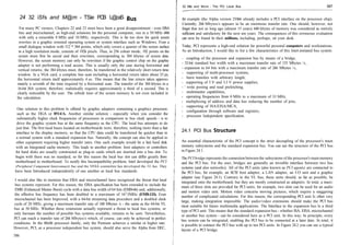
Table 24.2: Use of the PCI block access modes Figure 243: The PCI read transfer burst. Contrary to the optimum 3 - 2 - 2 - 2 - . . . burst, a 3-1-2-2 burst is
shown, whereby in the first instance an inactive TRDY, and in the second instance an inactive IRDY, requests a
wait state. The addressed PCI unit reacts with an active DEVSEL signal, if it has identified itself as the target of
For extensive sequential write accesses, the memory write access with invalidation should be the PCI transfer. The transfer (3-1-2-2 burst) is ended by the deactivation of FRAME.
used as far as possible. However, a register for the cache line size is required for this in the
initiator.
Note that for memory accesses, address bits ADI and ADO are not decoded for the addressing.
PCI always addresses double words; the active bytes within a double word are then given by
BEx. ADI and ADO, however, are not without purpose; they are very important for setting the
addressing sequence. For all burst accesses, PCI makes a distinction between linear and toggle
incrementations of the addresses: linear incrementation (ADI = ADO = 0) means that all ad-
dresses follow one another sequentially; toggle incrementation (ADI = 0, ADO = 1) means that
the addresses follow in the style of a cache line fill, for instance they are interleaved as in the
Pentium, and thus do not follow one another sequentially.
In Figure 243 you can see the flow of the most important signals for a typical PCI read access.
Note that the first clock cycle after the address phase is used to switch the transfer direction DEVSEL
of the multiplexed PCI address/data bus. During the address phase, the ADx pins deliver a
value (the address), while during the data phase they receive a value (read data). As in the
8086/83, with its multiplexed address/data bus, a dummy cycle is required for the change
in direction. Thus, the first value can be transferred in the third PCI clock cycle at the earliest.
Figure 24.4: The PCI write transfer burst. Contrary to the optimum 2 - 2 - 2 - 2 - . . . burst, a 2-1-2-2 burst is
The PCI read transfer burst is, therefore, most economically performed (not wait states) as a shown, whereby in the first instance an inactive TRDY, and in the second instance an inactive IRDY, requests a
3-1-1-1- . . . burst. wait cycle. The addressed PCI unit reacts with an active DEVSEL signal, if it has identified itself as the target of
the PCI transfer. The transfer (2-1-2-2 burst) is ended by the deactivation of FRAME.
A typical PCI write access is performed in a similar way. It is also initiated by the activation of
FRAME. In Figure 24.4, the flow of the most important signals is shown. Here, contrary to a read
access, the multiplexed PCI address/data bus need not be switched. The data phase can follow
immediately after the address phase, without the need for a dummy cycle. Thus, the first value
can be transferred in the second PCI clock cycle. The PCI read transfer burst is most economic-
ally performed (no wait cycles) as a 2-1-1-1-. . . burst.
6. 596 32 Bits and More - The PCI Local Bus 597
Chapter 24
243 Bus external busmaster located on the adapter Is a form of DMA controller which quickly exchanges
data between the main memory and the adapter. The busmaster concept is, therefore, more
PCI bus arbitration Is performed separately for each access, that is, a busmaster cannot hold up generally understood than the Direct Memory Access, but DMA Is only part of the busmaster
the PCI bus between two accesses. This may occur with EISA and MCA. For this reason, a PCI concept.
burst, which In the sense of bus arbitration represents a single access, can extend over any
number of transfer cycles. However, this single arbitration does not impair the transfer band-
width of the PCI bus because the arbitration Is «hidden» behind the active bus; a hidden arbitra-
tion takes place. This means that the arbitration is already being performed if the active bus
access is still running. In this way, no PCI bus cycles are required for the arbitration. Only optional interrupts are Included In the PCI specification; they should be level-triggered
and active-low. One Interrupt line, INTA, is assigned to each PCI unit. Only multifunctional
PCI includes two control signals for arbitration: REQ and GNT. Each busmaster has Its own
units can also use the other three Interrupt lines INTB, INTC and INTD. The PCI Interrupts are
request and grant signals, which are intercepted and used by a central arbitration logic. How-
formed in the CPU PCI bridge like the interrupt requests IRQx of the AT architecture. This
ever, the PCI specification does not lay down a model for the arbitration; this Is a task for the
usually occurs In a flexible way with help from the setup in the computer BIOS. Depending on
system designer. Usually, a model corresponding to the CACP from microchannel, or the bus
which slot a PCI IDE hard disk adapter is installed in, the corresponding Interrupt INTA for
arbitrators from EISA are used. The PCI specification only requires that a PCI busmaster must
this slot must be set to the IRQ14 of the AT architecture. The INTA of a different slot (with, for
activate the REQ signal to Indicate a request for the PCI bus, and the arbitration logic must
example, a LAN adapter) can then be set to a different AT IRQx, for instance, IRQ11. Thus, for
activate the GNT signal so that the requesting master can gain control of the bus. The busmaster
a single function PCI unit, only one interrupt (namely INTA) is available for each slot; whereas
must then begin a bus transfer within 16 CLK cycles, otherwise a time overrun error occurs.
for a multifunction agent, one to four are available (INTA to INTD). The actual IRQ activated
by the PCI Interrupt Is set by software configuration. In this way, the Inflexible setting of the
IRQs, as in the AT architecture and also EISA /MCA, is no longer applicable. In addition, fewer
24.4 DMA contacts are needed - ISA /EISA /MCA slots contain 11 contacts without an increase in function-
ality. In a typical ISA/EISA/MCA adapter, ten contacts are not utilized; in a typical PCI adapter
If you look at the layout of the PCI slots (Section 24.9) and the specific PCI signals (Section only three are not used (with which the adapter activates more than just an IRQ).
24.11), you can see that contrary to ISA/EISA and microchannel, no Direct Memory Access
(DMA) is implemented. The «normal» DREQx and DACKx signals known from the PC are
missing. At first, this may appear as a backward step because, above all In EISA and MCA PCs, is Space
the transfer of large quantities of data from peripheral devices to the main memory, and vice
versa, can be performed very quickly via a DMA (even though PC manufacturers very rarely
According to its specification, the PCI bus supports a 32-bit and also a 64-bit I/O address area.
use this channel). The busmaster concept (not only In PCI, but also in EISA and microchannel)
However, this only applies to true PCI units. You cannot reach an address greater than 64k with
actually makes direct memory accesses superfluous. The DMA controller Is usually located on
an 80x86 CPU because these processors can only produce 16-bit I/O addresses. The ports In a
the motherboard, but typically controls an I/O unit located on an adapter (such as the hard disk
personal computer with a PCI bus are all located below 64k; the usage and address of each port
controller). In this way, the data transfer is triggered, for example, by the DREQ signal (single
have not changed when compared to ISA/EISA and MCA, depending on whether your PC is
transfer mode). However, the necessary bus control signals (such as IOW, MEMR, etc.) are
based on the AT, EISA or PS/2 architecture, or a standard expansion bus with either ISA/EISA
produced by the DMA controller (as busmaster) itself, that is, the CPU is not Involved with the
or microchannel. ISA/EISA/MCA and PCI can, and should, be available alongside each other
data transfer. Stated another way, you could regard the combined efforts of the (busmaster)
as PCI and the expansion bridge make this possible. You will find all of the valid I/O addresses
DMA controller and of the trigger signal DREQ as a busmaster function of the adapter, where
and their corresponding usage in Chapters 21 (ISA), 22 (EISA) and 23 (MCA).
the busmaster chip is generally located on the motherboard where the bus control signals are
produced, while the adapter uses this second busmaster In addition to the CPU through its PCI stores two PCI registers in an I/O address area, which in EISA are reserved for the
DREQ signal. A single busmaster chip on the adapter Itself makes this somewhat complicated motherboard. These two 32~bit registers CONFIG_ADDRESS and CONFIG_DATA are used for
procedure superfluous. The adapter busmaster can now produce all of the bus control signals accessing the configuration address area and are located at the addresses 0cf8h (ADDRESS) and
itself and, thus, can address the I/O and memory address area In any number of ways. How- Ocfch (DATA). If you wish to read or write a double word in the configuration area of a PCI
ever, this requires bus arbitration by means of the expansion bus (or the slots), because with unit, you must transfer the corresponding address to the CONFIG_ADDRESS register first. A
the DMA, only the arbitration between the CPU and the DMA controller is performed on write to the CONFIG_DATA. register transfers the value to the specified location in the configur-
the motherboard. Thus, the use of an external busmaster is more flexible and efficient than the ation address area of the addressed unit; a read transfers the value from this location. You can
DMA, but makes a more complicated arbitration necessary. It Is, of course, possible that the see the layout of the address registers In Figure 24.5.
7. 593 Chapter 24 32 Bits and More - The PCI Local Bus 599
2 1 0 CSE Register (Port 0cf8h) Forward Register (Port Ocfah)
E 7 4 3 10 7 0
^SCE
! I I I I Pi I I I I I I I U
Key Function PCI Bus 1
Lhdblc GCi !< _l i
-i 011FIC_DA i io, n J ited 1 =C0NFIG_DAT A register activated
I/O Address
01 =CONFIG_ADDRESS value copy to ADx
31 16 15 12 11 8 7 2 10
I I I I I I I I I I I I I I I I I I I
Figure 245: The CONFIG_ADDRESS register. 0 0 0 0 0 0 0 0 0 0 0 0 0 0 0 0 1 1 0 0 PCI Unit Register Index 0 0 u
Key: 0000=Normal mode 0001 ..1111 =Configuration area activated
If you set the ECD bit, the bridge carries out a configuration cycle for the I/O address Ocfch SCE: Special cycle activation (Special Cycle Enable)
(corresponding to CONFIGJDATA). If the ECD bit Is not set, a normal I/O cycle is performed 0=Configuration cycle 1 =Special cycle
which does not reach the configuration address area; It Is switched through to the normal I/O
address area. The bus entry stores the number of the PCI bus in a hierarchically structured Figure 24.6: Activation register, forward register and I/O address for the configuration area.
system containing a maximum of 256 PCI buses. Such a hierarchically structured PCI bus sys~
tern can be Implemented by PCI-PCI bridges. Unit selects one of 32 possible PCI agents, function
one of a maximum of eight functions within a PCI multifunction unit. Then, register addresses ignored (It is better to set them to 00), address bits AD31-AD12 are equal to OOOOch or 0000 0000
one of 64 possible dword entries in a specified configuration address area. Type is used to inform 0000 0000 1100.
the bridge whether It is connected to the addressed unit (type = 0), and that after decoding of
In addition to these direct accesses to the configuration area of a PCI unit through the I/O ports,
the unit and function entries it should send out a configuration cycle. If type equals 01b, then
personal computers with a PCI bus, in general, also have an Interface available through the
the unit Is connected to the bridge and the bridge copies the contents of CONF1G_ADDRESS,
BIOS interrupt lah. Its standardized functions are detailed In Section 24.9. First, however, we
unchanged, to the address/data bus. An access to the configuration address area through the
shall look at the layout of the configuration address area.
two registers CONFIG_ADDRESS and CONFIGJDATA Is known as configuration mechanism #1
In this way you can also instruct a PCI bridge to send out a special cycle In which the PCI bridge
Is specified In the address register for the bus entry, the entries for unit and function are written
with a series of Is and the register entry Is written with a series of 0s. The next access to the data
24.7 Configuration Address Space
register then Initiates a special cycle, where AD31-AD0 transfer the data register value.
A configuration area of 256 bytes is provided for every PCI unit (and every separate function
In addition, there Is also a configuration mechanism #2, but this is only provided for PC systems in a multifunction unit), thus there are 64 registers for each 32 bits. A fixed header of 64 bytes is
(as a processor-Independent bus system, PCI can also be used in the Alpha or PowerPC, for located at the start, which is predefined for each unit with this structure. The use of the remain-
example). Here, the PCI configuration area of a PCI unit Is mapped Into a 4k I/O address range ing 192 bytes depends upon each individual PCI unit. The configuration software for such a unit
between cOOOh and cfffh. This is achieved by using the activation register CSE (Configuration then recognizes the use of this range. Figure 24.7 shows the layout of the configuration area and
Space Enable) for the configuration area at the port address OcfSh; you can see the structure in that of the header.
Figure 24.6, together with the layout of the forward register.
Authentic values for unit ID are between O O h and fffeh; the value ffffh indicates that a PCI
OO
A value other than zero for key activates the mapping of the configuration area, that is, all I/O unit is not installed. In this way, the start routine of the PCI BIOS can Identify all of the PCI
accesses with an address between cOOOh and cfffh initiate a configuration cycle. Otherwise, units. The entries In the configuration area follow the little-endian format. The header itself is
the I/O accesses to the 4k range between cOOOh and cfffh would be performed as normal I/O divided into two sections: the first 16 bytes (OOh to Ofh) are the same for all PCI units; the layout
cycles. The PCI bus entry In the forward register at the port address Ocfah indicates the PCI bus of the subsequent 48 bytes can vary for different PCI units. These layouts are differentiated by
for which the configuration cycle should be performed. A value of OOh means, for example, the the header entry (offset Oeh). Currently, only a single header type is defined (header = OOh),
bus Immediately after the host bridge. Now, If you write a value to the 4k I/O range between namely that you can see in the figure between offsets lOh and 3fh. The most significant header
cOOOh and cfffh, the address bits AD11-AD8 give the I/O address of the PCI unit, the function bit 7 indicates whether the unit Is multifunctional (bit 7 = 1) or single function (bit 7 = 0). Note
entry In the CSE register gives the function number within this PCI unit (If It represents a that the PCI specification only requires that the manufacturer ID, unit ID, command and status
multifunction unit), and the address bits AD7-AD2 give the I/O address of the register index entries are available. The manufacturer ID is allocated by PCI SIG (the governing body that
(or the dword register offset). The two address bits ADI and AiDO of the I/O address are produced the PCI standard). However, unit ID and revision are inserted by each manufacturer.
8. 600 601
Chapter 24 32 Bits and More - The PCI Local Bus
256 Byte Configuration Space 64 Byte Header Basic Meaning Subcode
31 16 15
code
Oh
O Unit was produced before the OOh All previous
class code definition was units except VGA
defined 01h VGA
O1h Controller for mass storage OOh SCSI controller
01h IDE controller
192 Bytes Available 02h Floppy controller
for PCI Unit 03h IPI controller
80h Other controller
02h Network controller OOh Ethernet
01h Token ring
02h FDD!
80h Other controller
03h Video controller OOh VGA
01h XGA
Figure 24.7: 256-byte configuration area and 64-byte header. 80h Other controller
O4h Multimedia unit OOh Video
01h Audio
The class code indicates the type of PCI unit. For this, the field is subdivided into three 1-byte 80h Other unit
sections. The most significant byte (at the offset Obh) indicates the basic class code, the middle 05h Memory controller OOh RAM
byte (at the offset Oah) indicates the subclass code, and the least significant byte (at the offset 01 h Flash memory
uO9h) delivers a programming interface for the applicable unit. The authentic basic and subclass 80h Other controller
06h Bridge OOh Host
codes are shown in Table 243.
01h ISA
02h EISA
For many previously defined basic and subclass codes, clearly defined programming interfaces
03h MCA
already exist (such as VGA or SCSI), so that here no programming interface through the least 04h PCi-PCl
significant byte (at the offset 09h) of the class code entry is required. For all other units, no such 05h PCMCIA
programming interface has been defined. For this reason, all detailed classes have the entry O h O 80h Other bridge
in the programming interface field. The instruction entry in the header makes it possible to 07h-eh Reserved
control the unit, that is, how it reacts to PCI cycles. Figure 24.8 shows the structure of this entry. ffh Unit does not belong to any none
class OOh-feh
If you write the value O O h to the instruction register, you deactivate the applicable PCI unit;
OO
then, it will only react to a configuration cycle. Table 243: Basic and subclass codes
A set BBE bit enables so-called fast «back-to-back» cycles for different targets. In this way, fewer
dummy cycles are required between two PCU bus transactions. The SEE bit activates (SEE = 1)
• or deactivates (SEE = 0) the driver for the SERR signal. Should the system control also be in- accordingly to them. If a unit should operate as a busmaster,you must set the BM,bit. When
formed of address parity errors, both SEE and PER must be set. The WC bit must be set for PCI MAR is set, the unit will react to an access of the memory address area, with a set IOR bit, It
units which perform address/data stepping. Address/data stepping means that not all neces- will react to I/O cycles. In addition to the instruction register, a status register Is also provided;
sary address/data signals are activated at one time. To reduce the load on the infernal driver it indicates the status of the applicable unit for a PCI operation. The layout of the register Is
during activation of the lines, they are gradually set to a high level by means of blocks over a given in Figure 24.9.
number of clock cycles. With this, the PCI units must wait a short time until all of the potentials If the unit discovers a parity error it sets the PER bit. The SER bit Is set if the unit activates the
have stabilized. If the PER bit is set, the PCI unit will react to a parity error; with a reset PER SERR signal If a unit operating as a busmaster stops a transaction, it must set the MAB bit. This
bit, all parity errors are Ignored. By setting the VPS bit, you instruct a VGA compatible PCI unit is similar for TAB, except that here, the target has stopped the operation. MAB and TAB are set
to ignore all accesses to the palette register. If VPS = 0, the unit will react normally. A set MWI by the busmaster. STAf on the other hand, Is set by a unit operating as the target if It has
bit permits the unit to send out a memory write access with invalidation; If MWI is reset, it initiated a target abort. The two DEVTIM bits set the time characteristic for the DEVSEL signal
must use a normal memory write access Instead. By resetting SCf you can Instruct the unit to The DP bit is only implemented for the busmaster, and Is set if PERR Is activated, the unit Is
Ignore all special cycles; If SC = 1, then the unit will also recognize special cycles, and will react operating as a busmaster, and the PER bit is set in the instruction register. Finally, the FBB bit
9. 602 Chapter 24 32 Bits and More - The PCI Local Bus 603
10 9 8 / 6 b
implemented for targets indicates whether the target supports fast back-to-back cycles (FBB = 1)
15 4 3 2 1 0
or not (FBB = 0).
i
| we
(PER
(SEE
I i I I I
SdAl
BBE
O£
Reserved CD O
The header entry CIS (cache line size) defines the cache line size of the system in units of 32
BBE:Fast back-to-back cycles (Back-to-Back Enable)
bytes. It is necessary, for example, for the memory write access.with invalidation instruction.
0=deactivate 1 =activate The latency entry indicates how long a PCI bus operation can take: the effective time span
SEE: SERR Enable amounts to the latency+8 PCI clock cycles. The most significant bit in the BIST (Built-in Self-
0=deactivate 1 =activate Test) register indicates whether the unit can carry out a self-test (bit 7 = 1). If that is the case, you
WC: Wait cycle control
can issue BIST by writing the value 1 to bit 6. BIST then returns a termination code to the four
0=no address/data stepping 1 =address/data stepping possible
PER: Parity error (Parity Error Response)
least significant BIST bits 3-0. Any value other than zero indicates an error. The header entry
0=ignore 1=perform INT-line in an AT PC indicates which hardware interrupt line IRQx is connected to the interrupt
VPS: VGA palette snoop pin of the unit or function. The values 0-15, corresponding to IRQ0-IRQ15, are valid. The
0=normal reaction 1 =no reaction interrupt routing logic of the PCI bridge then activates the corresponding input of the PIC.
MWI: Memory write access with invalidation
Which interrupt pin the unit or function actually uses is defined by the INT pin: a value of 1
0=deactivate 1 =activate
SC: Special cycle
means INT A, a value of 2 INTB, etc. If the unit does not use interrupts, you must enter the
0=ignore 1=include value 0. The two read-only registers MinGNT and MaxLat give the minimum and maximum
BM: Busmaster latency values required by the manufacturer of the PCI unit, so that the unit can optimally use
0=no 1=yes the PCI bus. Adapter and PCI units frequently contain an I/O or memory area, which they use,
MAR: Memory address area
for example, for storing data, program execution, etc. With the help of the base address register(s),
0=deactivate 1 =activate
lOR: I/O address area
PCI now allows these I/O and memory areas to be arranged in any I/O or memory address
0=deactivate 1 =activate area. In Figure 24.10, you can see the structure of the base address register for a 32/64-bit
memory base and a 32-bit I/O base. The memory address area can contain 32 or 64 bits, depending
Figure 24.8: Instruction register.
Base Address Register for Memory Address Space
63 32 31 16 15 4 3 2 1 0
15 14 13 12 11 10 9 I I I I I I I I I I I I I ! I I i I I I I I ! ! I I ! I
(PRF
Base Address Type 0
PER: Parity error Base Address Register for I/O Address Space
0=no parity error 1 =parity error found 31 16 15 2 1 0
SER: System error " 1 1 I 1 I I [ i | | | p IT li
Base Address 0 1
0=no system error 1 =system error signalled
MAB: Master abort
0=no master abort 1 =master abort received
TAB: Target abort Base Address Register for Expansion ROM
0=no target abort 1 =target abort received 31 16 15 11 10 2 1 0
I I I I I I T
STA: Target abort i I IT I IT I i I I i I i I I i i i r
0=no target abort 1 =target abort signalled
DEVTIM: DEVSEL timing
00=fast 01=medium 10=slow 11=reserved PRF: Prefetching
DP: Data parity error O=not possible 1 =prefetching possible
0=no parity error 1 =parity error found Type: Positioning type
FBB: Fast back-to-back cycles 00=any 32-bit address 01 =!ess than 1M
O=not supported 1 =supported 10=any 64-bit address 11 =reserved
AD: Address decoding and expansion ROM
Figure 24.9: Status register. 0=deactiva!ed 1 =activated
figure 24.10: Base address register for memory and I/O ports, and also expansion ROM base address.
10. 604
Chapter 24 32 Bits and More - The PCI Local Bus 605
on the implementation; the I/O address area, however, always has only 32 bits (of which the _ PCI BIOS available?
80x36 CPUs still only use the least significant address word AD15-AD0).
Bit 0 differentiates a memory base address (bit 0 = 0) from an I/O base address (bit 0 = 1). The function determines whether or not a PCI BIOS Is available.
Depending on the size of address, three to six base addresses are possible, the corresponding
entry in the header contains 24 bytes. First I would like to explain the entry for a memory base. Register Call value Return value
To be able to perform a remapping of an address area, the POST routine must naturally know
AH b1h 00h=available, O1h-ffh=not available1)
how large the area to be formed should be. For this purpose, all bits in the applicable base 01h Configuration mechanism, special cycles2)
AL
register which, in practice, represent an offset within the address area to be formed, are hard- BH Version (main level)
wired with the value 0. The POST routine can then simply determine the size of the area, BL Version (sub level)
whereby it writes the base address with a series of Is and then reads back the base address CL Number of the last PCI bus in the system
EX
D String "PCI" ('P' in DL, 'C in DH etc.)
value. All bits which return the value 0 are located within the address area to be formed; all bits
Carry Status: 1=no PCI BI0S1)
set to 1 should be affected by the remapping, if, for example, bits 15 to 4 return the value 0 and
the bits 31 (or 63) to 16 return the value 1, the area to be mapped encompasses 64 kbytes, 1)
PCI BIOS only available, if EDX also equals "PCI"
because the 16 least significant bits can address 216 bytes = 64 kbytes (the four least significant 2)
Bit 0=1: configuration mechanism #1, bit 1=1: configuration mechanism #2, bit 4=1: special cycle through configuration
mechanism #1, bit 5=1: special cycle through configuration mechanism #2
bits 3-0 cannot be changed, but are included for determining the size of the area). The remapping
is performed, whereby the POST routine overwrites the address bits which returned the value
1 with the required base address. As you can see, the remapping is performed in blocks of
- PCI unit search
16 bytes, 32 bytes, 64 bytes,. . ., 1 kbyte, 2 kbytes, etc. As the base address entry in the header
can include a number of base addresses, it also enables a fragmented remapping to be realized. The function determines, by means of the unit and manufacturer identification, and also an
If the PRF bit is set, the unit permits prefetching, that is, the bridge can read data in advance from index N, the PCI address of the unit, that is, bus number, unit number and function number of
the unit into a buffer without disturbing the unit or causing detrimental side-effects to occur. the Nth unit which fulfils the search criteria.
The 2-bit type entry indicates the address area where the mapping can be performed. The value
00b means that a 32-bit register can be mapped anywhere in the 32-bit address area; the value
Register Call value Return value
10b has a similar meaning, only here the register and the address area each contain 64 bits. The
AH b1h Result code in accordance with Table 24.4
value 01b is provided for 32-bit registers which must be formed in a 20-bit address below 1M.
AL 02h
The remapping for I/O addresses is achieved in a similar way, except that here only the two BH Bus number
least significant bits 1 and 0 remain unchanged (bit 0 = 1 indicates that mapping In an I/O BL Bits 7.3: unit, bits 2..0: function
address area will be carried out). Thus, I/O address areas can be mapped in units of 2 bytes, CX Unit
4 bytes, etc. A remapping of 2 bytes usually means that a single 32-bit I/O port will be placed DX Manufacturer
SI Index
in a suitable position in the I/O address area. Carry 1=error, 0=o.k.
As the last entry In the header, you will also find the expansion ROM base address. With this, you
can shift a ROM expansion to any position In a 32-bit memory address area. The remapping is
achieved In exactly the same way as for a 32-bit base address, only here the 21 most significant ~ PCI class code search
bits are provided for the remapping. Thus, ROMs can occur and be remapped in units of The function determines, by means of a specific class code, the PCI address of the Nth unit
2 kbytes, 4 kbytes, etc. By setting ADf you activate the expansion ROM, that Is, addresses are which contains this class code.
decoded; the value zero deactivates the ROM expansion. In this way, a PCI unit can operate
with or without a ROM expansion selected. Only if AD Is set does the remapping address in bits
32-11 have any significance. Register Call value Return value
AH b1h Result code in accordance with Table 24.4
AL 03h
BH Bus number
BL Bits 7.3: unit, bits 2..0: function
ECX Class code
You can comfortably access the configuration address area with ten functions of the BIOS SI Index
interrupt lah. They are listed in the following section along with brief explanations. Carry 1=error, 0=o.k.
11. 606
32 Bits and More - The PCI Local Bus 607
- Initiate special cycle
All functions return a result code In register AH. The five possible PCI BIOS result codes are
The function sends out a special cycle to a specific PCI bus in the system. The 32~bit value listed in Table 24.4.
EDX is sent on the address/data bus ADx during the data phase.
Code Meaning
Register Call value Return value OOh Successful completion
AH b1h 81 h Function not supported
Result code in accordance with Table 24.4
AL 06h 83h Invalid manufacturer identification
BH Bus number 86h Unit not found
EDX Data 87h Invalid register number
Carry 1=error, 0=o.k.
24.4: PCI BIOS result codes
- Configuration byte/word/double word read
24.9 PCI Slots : •
PCI frees itself not only from ISA - as microchannel did a few years previously - but with its
slot geometry and contact layout, it is entirely Independent from all existing bus systems. Only
Register the dimensions of the slots bring microchannel to mind. PCI is laid out for an address and data,
Call value Return value
bus width of 32 bits without compromise; you are wasting your time looking for 8-bit and 16-
AH b1h Result code in accordance bit segments. Instead, an expansion increase to 64 bits is planned. You can see the construction
with Table 24.4 and signal layout of a PCI slot In Figure 24.11. The multiplexing scheme for the data and
AL 08h (byte), 09h (word),
Oah (dword) address bits can clearly be seen. In total, a maximum of three PCI slots can be available. How-
BH Bus number ever, as each slot can be filled by a PCI adapter containing a number of functional units and,
BL Bits 7.3: unit, in addition, PCI units can also be included on the motherboard, the quantity of possible PCI
bits 2..0: function devices is not restricted to three. With a PCI clock speed of 33 MHz and the high current driving
CL/CX/ECX Read byte, word, dword
D! Register number
capabilities which adapters request compared to on-board units, more than three external adapters
Carry 1=error, 0=o.k. would overload the PCI components, or would become too error-prone.
The 32-bit section contains 124 contacts, of which, however, only 120 are actually used. The
- Configuration byte/word/double word write remaining four contacts are blocked by a code bridge. Owing to the different slots, PCI takes
into account the technical developments initiated for the 3.3 V technology used in power saving
The three functions write a byte (8 bits), word (16 bits) or double word (32 bits) Into the configur- notebooks or green PCs. In this way, the power consumption in a CMOS circuit can be halved.
ation area of a PCI unit. This is because the power consumption is proportional to the square of the supply voltage.
Some highly integrated circuits go one stage further, and can no longer even tolerate the normal
Register Call value
5 V supply, because their internal structure (above all, the channel width of the MOSFETs)
Return value
would burn. A further PCI demand with respect to lower power consumption is that every PCI
AH b1h Result code in accordance unit must operate with a clock between 0 MHz and 33 MHz. In this way, for example, the clock
with Table 24.4 signal can be switched off (0 MHz) to reduce the power consumption by more than 99.9%.
AL Obh (byte), Och (word),
Odh (dword)
BH Bus number The two present contacts PRSNT1 and PRSNT2 are individually, or jointly, connected to ground
BL Bits 7.3: unit, or left open by an installed PCI adapter, in order to indicate that an adapter is installed and
bits 2..0: function what its power consumption is. If no adapter Is installed, then both contacts naturally remain
CL/CX/ECX Write byte/word/dword open. The possible configurations are shown in Table 24.5.
D! Register number
Carry 1=error, 0=o.k. The pins identified as I/O represent special supply pins for a universal adapter, which can be
operated with both 5 V and 3.3 V. Such adapters can be Inserted Into any slot. Note that In