

Recomendados
Más contenido relacionado
La actualidad más candente
La actualidad más candente (20)
Similar a quantum dots
Similar a quantum dots (20)
Más de Hoang Tien
Más de Hoang Tien (17)
Último
Último (20)
quantum dots
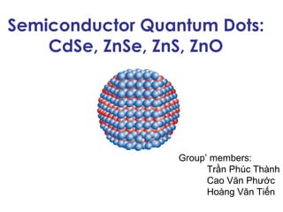
- 1. Semiconductor Quantum Dots: CdSe, ZnSe, ZnS, ZnO Group’ members: Trần Phúc Thành Cao Văn Phước Hoàng Văn Tiến
- 2. Outline • Introduction – What is semiconductor quantum dots – Why quantum dots – Properties • Synthesis • Applications, challenges, and potentials • Conclusions
- 3. Introduction: Image courtesy of Dr. D. Talapin, University of Hamburg
- 4. What is Quantumdots? • Quantum dots are semiconductor nanocrystals. • They are made of many of the same materials as ordinary semiconductors (mainly combinations of transition metals and/or metalloids). • Unlike ordinary bulk semiconductors, which are generally macroscopic objects, quantum dots are extremely small, on the order of a few nanometers. They are very nearly zero- dimensional.
- 5. Exciton Bohr Diameter • Material Dependent Parameter – The same size dot of different materials may not both be quantum dots • The Bohr Diameter determines the type of confinement – 3-10 time Bohr Diameter: Weak Confinement – Smaller than 3 Bohr Diameter: Strong Confinement
- 6. Experimental Observation of Confinement • Just imaging a small dot is not enough to say it is confined • Optical data allows insight into confinement – Optical Absorption – Raman Vibration Spectroscopy – Photoluminescence Spectroscopy
- 7. Optical Absorption • Optical Absorption is a technique that allows one to directly probe the band gap • The band gap edge of a material should be blue shifted if the material is confined • Bukowski et al. present the optical absorption of Ge quantum dots in a SiO2 matrix. • As the dot decreases in size there is a systematic shift of the band gap edge toward shorter wavelengths
- 8. Raman Vibrational Spectroscopy • Raman vibrational spectroscopy probes the vibrational modes of a sample using a laser • As the nanocrystal becomes more confined the peak will broaden and shrink • Here we see a peak shift toward the laser line • Various Ge dots of different sizes on an Alumina film
- 9. Direction of Raman Shift • Here we see the same broadening and shrinking of the Raman Peak • We see a peak shift away from the laser line • No systematic shift of the Raman line – Shifts toward the laser line are due to confinement – Shifts away from the line are due to lattice tension due to film miss-match
- 10. Photoluminescence Spectroscopy • Photoluminescence spectroscopy is a technique to probe the quantum levels of quantum dots • Here we see dots of various size in a quantum well – (a) is quantum well spectrum – (d) is smallest particles 80 nm
- 11. Properties of Quantum Dots Compared to Organic Fluorphores? High quantum yield; often 20 times brighter Narrower and more symmetric emission spectra 100-1000 times more stable to photobleaching High resistance to photo-/chemical degradation Tunable wave length range 400-4000 nm CdSe CdTe http://www.sussex.ac.uk/Users/kaf18/QDSpectra.jpg J. Am. Chem. Soc. 2001, 123, 183-184
- 12. Why
- 13. Excitation in a Semiconductor The excitation of an electron from the valance band to the conduction band creates an electron hole pair E ECB hυ E =g − ( ) + ) h↔ BhV υ e C+ ( B Creation of an electron hole pair where hν is the photon energy EVB semiconductor Band Gap optical detector (energy barrier) E=hυ exciton: bound electron and hole pair usually associated with an electron trapped in a localized state in the band gap
- 14. Recombination of Electron Hole Pairs Recombination can happen two ways: radiative and non-radiative E ECB recombination processes EVB E band-to-band recom bination recom bination atinterband trap states ECB (e.g. dopants, impurities) E = hυ radiative recombination → photon EVB non-radiative recombination → phonon (lattice vibrations) − ) + ) υ ra d ia tive n o n -ra d ia tive re co m b in a tio n re c o m b in a tio n e C+ ( B h ( BhV→
- 15. Effective Mass Model Developed in 1985 By Louis Brus Relates the band gap to particle size of a spherical quantum dot Band gap of spherical particles The average particle size in suspension can be obtained from the absorption onset using the effective mass model where the band gap E* (in eV) can be approximated by: − π .e 1 h2 1 1 1 03 1 1 2 8 .42e 1 E + + = − − + *b u l k E 2 m hπ h 2 ε 0 h m ε ( 0m m ) m ε 4 2e m g 0 2 e e r 0 m 04 r π ε m0 Egbulk - bulk band gap (eV), h - Plank’s constant (h=6.626x10⁻³⁴ J·s) r - particle radius e - charge on the electron (1.602x10⁻¹⁹ C) me - electron effective mass ε - relative permittivity mh - hole effective mass ε0 - permittivity of free space (8.854 x10⁻¹⁴ F cm-1) m0 - free electron mass (9.110x10⁻³¹ kg) Brus, L. E. J. Phys. Chem. 1986, 90, 2555
- 16. Term 1 The second term on the rhs is consistent with the particle in a box quantum confinement model Adds the quantum localization energy of effective mass me High Electron confinement due to small size alters the effective mass of an electron compared to a bulk material Consider a particle of mass m confined P oten tia l E nergy in a potential well of length L. n = 1, 2, … For a 3D box: n2 = nx2 + ny2 + nz2 2 π n h2 2 n h 22 E= n 2 = x 2 L 8 L m m2 0 L − h 1 1 1e . 2 0 2e 1 1 2 1 8 . 44 1 E = g lk+ 2 * Eu b + − − + r m 0 m 0 4 ε 0 h ( ε 0 2 e 0 m 0 8 em hm πεr 2 2ε ) m m hm Brus, L. E. J. Phys. Chem. 1986, 90, 2555
- 17. Term 2 The Coulombic attraction between electrons and holes lowers the energy Accounts for the interaction of a positive hole me+ and a negative electron me- Electrostatic force (N) between two charges (Coulomb’s Law): qq F= 1 2 2 Work, w = ∫F·dr εε 4π 0r Consider an electron (q=e-) and a hole (q=e+) The decrease in energy on bringing a positive r charge to distance r from a negative charge is: 2 2 e e ∆ =∫ E d= r − 4 ε0 πε r2 4 ε0 πε r − h 1 1 1e . 2 0 2e 1 1 2 1 8 . 44 1 E = g l + 2 * Euk b + − − + r m 0 m 0 4 ε 0 h ( ε 0 2 e 0 m 0 8 em hm πεr 2 2ε ) m m hm Brus, L. E. J. Phys. Chem. 1986, 90, 2555
- 18. Term Influences The last term is negligibly small Term one, as expected, dominates as the radius is decreased Energy (eV ) Modulus 1 term 1 term 2 term 3 0 0 5 10 d (nm) Conclusion: Control over the particle’s fluorescence is possible by adjusting the radius of the particle
- 19. Quantum Confinement of ZnO ZnO has small effective masses quantum effects can be observed for relatively large particle sizes Confinement effects are observed for particle sizes <~8 nm ZnO CdSe ZnO λbulk = 365 nm λbulk = 709 nm ε = 8.66 ε = 10.6 Eg (eV) 4 me* = 0.24 me* = 0.13 mh* = 0.59 mh* = 0.45 3 400 λ onset (nm) 350 300 250 0 5 10 d (nm)
- 20. Fabrication Methods • Goal: to engineer potential energy barriers to confine electrons in 3 dimensions • 3 primary methods – Lithography – Colloidal chemistry – Epitaxy
- 21. 2. Fabrication of Quantum Dots How to Make Quantum Dots • There are three main ways to confine excitons in semiconductors: – Lithography – Colloidal synthesis – Epitaxy: » Patterned Growth » Self-Organized Growth 21
- 22. 2. Fabrication of Quantum Dots Lithography • Quantum wells are covered with a polymer mask and exposed to an electron or ion beam. • The surface is covered with a thin layer of metal, then cleaned and only the exposed areas keep the metal layer. • Pillars are etched into the entire surface. • Multiple layers are applied this way to build up the properties and size wanted. • Disadvantages: slow, contamination, low density, defect formation. Resulting quantum dot etched in GaAs/AlGaAs superlattice. 22 L. Jacak, P. Hawrylak, A. Wojs. Quantum dots fig. 2.2.
- 23. 2. Fabrication of Quantum Dots Colloidal Synthesis • Immersion of semiconductor microcrystals in glass dielectric matrices. • Taking a silicate glass with 1% semiconducting phase (CdS, CuCl, CdSe, or CuBr). • Heating for several hours at high temperature. ⇒ Formation of microcrystals of nearly equal size. • Typically group II-VI materials (e.g. CdS, CdSe) • Size variations (“size dispersion”). 23
- 24. 2. Fabrication of Quantum Dots Epitaxy: Patterned Growth • Semiconducting compounds with a smaller bandgap (GaAs) are grown on the surface of a compoundwith a larger bandgap (AlGaAs). • Growth is restricted by coating it with a masking compound (SiO2) and etching that mask with the shape of the required crystal cell wall shape. • Disadvantage: density of quantum dots limited by mask pattern. L. Jacak, P. Hawrylak, A. Wojs. Quantum dots 24 fig 2.7.
- 25. 2. Fabrication of Quantum Dots Epitaxy: Self-Organized Growth • Uses a large difference in the lattice constants of the substrate and the crystallizing material. • When the crystallized layer is thicker than the critical thickness, there is a strong strain on the layers. • The breakdown results in randomly distributed islets of regular shape and size. • Disadvantages: size and shape fluctuations, ordering. Schematic drawing of lens-shaped self- organized quantum dot. L. Jacak, P. Hawrylak, A. Wojs. Quantum dots 25 fig 8.1.
- 26. Lithography • Etch pillars in quantum well heterostructures – Quantum well heterostructures give 1D confinement • Mismatch of bandgaps ⇒ potential energy well – Pillars provide confinement in the other 2 dimensions • Electron beam lithography • Disadvantages: Slow, contamination, low density, defect formation A. Scherer and H.G. Craighead. Fabrication of small laterally patterned multiple quantum wells. Appl. Phys. Lett., Nov 1986.
- 27. Colloidal Particles • Engineer reactions to precipitate quantum dots from solutions or a host material (e.g. polymer) • In some cases, need to “cap” the surface so the dot remains chemically stable (i.e. bond other molecules on the surface) • Can form “core-shell” structures • Typically group II-VI materials (e.g. CdS, CdSe) • Size variations ( “size dispersion”) CdSe core with ZnS shell QDs Red: bigger dots! Blue: smaller dots! Evident Technologies: http://www.evidenttech.com/products/core_shell_evidots/overview.php Sample papers: Steigerwald et al. Surface derivation and isolation of semiconductor cluster molecules. J. Am. Chem. Soc., 1988.
- 28. Epitaxy: Patterned Growth • Growth on patterned substrates – Grow QDs in pyramid-shaped recesses – Recesses formed by selective ion etching – Disadvantage: density of QDs limited by mask pattern T. Fukui et al. GaAs tetrahedral quantum dot structures fabricated using selective area metal organic chemical vapor deposition. Appl. Phys. Lett. May, 1991
- 29. Epitaxy: Self-Organized Growth • Self-organized QDs through epitaxial growth strains – Stranski-Krastanov growth mode (use MBE, MOCVD) • Islands formed on wetting layer due to lattice mismatch (size ~10s nm) – Disadvantage: size and shape fluctuations, ordering – Control island initiation • Induce local strain, grow on dislocation, vary growth conditions, combine with patterning AFM images of islands epitaxiall grown on GaAs substrate. (a) InAs islands randomly nucleate. (b) Random distribution of InxGa1xAs ringshaped islands. (c) A 2D lattice of InAs islands on a GaAs substrate. P. Petroff, A. Lorke, and A. Imamoglu. Epitaxially self-assembled quantum dots. Physics Today, May 2001.
- 30. APPLICATIONS
- 31. Quantum computing A quantum computer is a computer design which uses the principles of quantum physi to increase the computational power beyond what is attainable by a traditional compute
- 32. The tiny seven-atom quantum dot created by scientists (left), with a close-up of that dot forming an atomic-scale transistor (right) essential for the creation of semiconductorbased quantum computers, which could be faster and provide more memory than conventional technology.
- 33. Rules: -By applying small voltages to the leads, the flow of electrons through the quantum dot can be controlled and thereby precise measurements of the spin and other properties therein can be made. -With several entangled quantum dots, or qubits , plus a way of performing operations, quantum calculations and the computers that would perform them might be possible. Bits :a bit can be defined as a variable or computed quantity that can have only two possible values : 0/1 or on/off… Qubits: -quantum mechanics allows the qubit to be in a superposition of both states at the same time, a property which is fundamental to quantum computing. - a qubit can be 0, 1, or a superposition of both.
- 34. Quantum-dot light-emmiting diodes ( QDLED)
- 35. -The spectrum of photon emission is narrow, characterized by its full width at half the maximum value -pure and saturated emission colors with narrow bandwidth - emission wavelength is easily tuned by changing the size of the quantum dots
- 36. • Advantages : – Low power consumption – Ranger and accuracy color – Brightness: 50~100 times brighter than CRT and LCD displays ~40,000 cd/m2 – QLED screens are said to be twice as power efficient as OLED screens, and offer 30 to 40% improved brightness. • Disadvantages : – Less saturated blue – expensive
- 37. Quantum dot solar cell • Quantum dots have bandgaps that are tunable across a wide range of energy levels by changing the quantum dot size.
- 38. 5–20 layer QD-enhanced solar cells show a net increase in external quantum efficiency (EQE) at IR wavelengths compared to the baseline GaAs
- 39. How Can Quantum Dots Improve the Efficiency? • Quantum dots can generate multiple exciton (electron- hole pairs) after collision with one photon. 39 39
- 40. Spincast quantum dot solar cell roll-to-roll solar cell fabrication. • Results: – -conversion efficiencies up to a record-breaking 7 percent efficiency. – The efficiency of solar cells could be increased to more than 60% from the current limit of just 30%...
- 41. Another applications • Photodetector devices • Quantum dots laser • Colloidal quantum dots • Uses in biology:use of QDs as passive labels in sensor applications, gene technology, pathogen and toxin detection…
- 42. Challenges and potentials • Potentials : – The composition and very small size of quantum dots (5–8 nm) gives them unique and very stable fluorescent optical properties that are readily tunable by changing their physical composition or size. – Their broad absorption spectra but very narrow emission spectra allows multiplexing of many quantum dots of different colors in the same sample. – quantum dots can be made from many different elements, and come in many different shapes and sizes, • Challenges : – Hard to control the side of dots. – Cytotoxic Effect – Environmental toxicity: • Phytotoxicity • Marine toxicity
- 43. conclusion • Quantum dot are the new and inovative perspective on the traditional semiconductor • Quantum dot can be synthesized to be essentially any size, and therefore produce essentially any wavelength of light • Application of Quantum Dots that they are useful in many conditions due to their physiochemical properties Quantum Dots may used in different fields by altering their surface property, internal structures, preparation techniques, coating material etc. • The future looks bright and exciting on all the possible applications of quantum dots
- 44. references 1, http://en.wikipedia.org/wiki/Quantum_dot 2. http://nature.com 3. http://google.com 4. Y. Masumoto and T. Takagahara. Semiconductor Quantum Dots: Physics, Spectroscopy, and Applications. New York: Springer-Verlag, 2002. 5. Synthesis and Applications of Nanoparticles and Quantum Dots-Richard D. Tilley 6. http://www.nanowerk.com 7. http://led-professional.com 8. http://quantumdotstech.com/ 9. http://youtube.com ………
Notas del editor
- Quantum dots created on the surface of GaAs in selective MOCVD growth ( metallorganic vapor phase epitaxy) ; width of the electron localization area at the top of the pyramid is about 100 nm.
- A quantum computer is a computer design which uses the principles of quantum physics to increase the computational power beyond what is attainable by a traditional computer. Conventional computers are built from silicon chips that contain millions or billions of miniature transistors. Each of these can be turned "on" or "off" to represent a value of either "1" or "0". Conventional computers subsequently store and process data using "binary digits" or "bits". In contrast, quantum computers work with "quantum bits" or " qubits ". These are represented in hardware using quantum mechanical states rather than transistors that are turned "on" or "off". For example, quantum computers may use the spin direction of a single atom to represent each qubit, or alternatively the spin direction of a single electron or the polarization orientation of a photon. Yet other quantum computing designs supercool rare metals to allow qubits to be represented by the quantum spin of a tiny magnetic field. Due to the peculiar laws of quantum mechanics, individual qubits can represent a value of "1", "0" or both numbers simultaneously. This is because the sub-atomic particles used as qubits can exist in more than one state -- or "superposition" -- at exactly the same point in time. By attaching a probability to each of these states, a single qubit can therefore process a wide range of values. In turn, this allows quantum computers to be orders of magnitude more powerful than their conventional, purely digital counterparts. The fact that qubits are more "smears of probability" than definitive, black-and-white certainties is exceptionally weird. Flip a coin and it cannot come up both heads and tails simultaneously, and yet the quantum state of a qubit can in some senses do just that. It is therefore hardly surprising that renowned nuclear physicist Niels Bohr once stated that "anyone who is not shocked by quantum theory has not understood it!" Another very bizarre thing is that the process of directly observing a qubit will actually cause its state to "collapse" to one or other of its superpositions. In practice this means that, when data is read from a qubit, the result will be either a "1" or a "0". When used to store potentially infinite amounts of "hidden" quantum data, qubits can therefore never be directly measured. This means that quantum computers need to use some of their qubits as "quantum gates" that will in turn manipulate the information stored and processed in other hidden qubits that are never directly measured or otherwise observed. Because qubits can be used to store and process not just the digital values of "1" and "0", but also many shades of grey in between, quantum computers have the potential to perform massively parallel processing. This means that quantum computers will be very effective at performing tasks -- like vision recognition, medical diagnosis, and other forms of artificial intelligence processing -- that can depend on very complex pattern matching activities way beyond the capabilities of both traditional computers and most human beings.
- Today's computers work by representing information as a series of ones and zeros, or binary digits called "bits.“ This code is relayed by transistors, which are minute switches that can either be on or off, representing a one or a zero, respectively. Quantum computers would take advantage of a strange phenomenon described by quantum theory: Objects, such as atoms or electrons, can be in two places at the same time, or they can exist in two states at the same time. That means computers based on quantum physics would have quantum bits, or "qubits," that exist in both the on and off states simultaneously, making it possible for them to process information much faster than conventional computers. Each quantum dot, like each transistor in a conventional computer, is like a switch that defines a single qubit. Because electrons are said to have a "spin" of either up or down, the direction of spin can be used instead of the on or off positions of a conventional computer circuit.
- An applied electric field causes electrons and holes to move into the nanocrystal layer, where they are captured in the quantum dots and recombine, emitting photons.
- This property makes quantum dots attractive for multi-junction solar cells, where a variety of different energy levels are used to extract more power from the solar spectrum.
- Energy conversion efficiency (η) is the ratio between the useful output of an energy conversion machine and the input, in energy terms.
- Energy conversion efficiency (η) is the ratio between the useful output of an energy conversion machine and the input, in energy terms.