SlideShare una empresa de Scribd logo
1 de 19
Descargar para leer sin conexión
November 2008 Rev 4 1/19
1
STV8172A
Vertical deflection booster for
3 App TV/monitor applications with 70 V flyback generator
Features
■ Power amplifier
■ Flyback generator
■ Stand-by control
■ Output current up to 3.0 App
■ Thermal protection
Description
Designed for monitors and high performance TVs,
the STV8172A vertical deflection booster delivers
flyback voltages up to 70V.
The STV8172A operates with supplies up to 35V
and provides up to 3 APP output current to drive
the yoke.
The STV8172A is offered in a Heptawatt plastic
package.
In double-supply applications, a stand-by state
will be reached by stopping the (+) supply alone.
Figure 1. Heptawatt package
Figure 2. STV8172A pin detail
Heptawatt
(Plastic Package)
ORDER CODE: STV8172A
7
6
5
4
3
2
1
Tab connected
Input (Non Inverting)
Output Stage Supply
Output
Ground
Flyback Generator
Supply Voltage
Input (Inverting)
to pin 4
7
Thermal
Protection
6
4
3
5
STV8172A
+
-
Power
Amplifier
1
Flyback
Generator
Non-Inverting
Inverting
Input
Input
Ground or Negative Supply
Output
Flyback
Generator
Output Stage Supply
VoltageSupply
2
www.st.com
Obsolete Product(s) - Obsolete Product(s)
Contents STV8172A
2/19
Contents
1 Absolute maximum ratings . . . . . . . . . . . . . . . . . . . . . . . . . . . . . . . . . . . 3
2 Thermal data . . . . . . . . . . . . . . . . . . . . . . . . . . . . . . . . . . . . . . . . . . . . . . . 4
3 Electrical characteristics . . . . . . . . . . . . . . . . . . . . . . . . . . . . . . . . . . . . . 5
4 Application hints . . . . . . . . . . . . . . . . . . . . . . . . . . . . . . . . . . . . . . . . . . . . 7
4.1 DC-coupled application . . . . . . . . . . . . . . . . . . . . . . . . . . . . . . . . . . . . . . . 7
4.1.1 Application hints . . . . . . . . . . . . . . . . . . . . . . . . . . . . . . . . . . . . . . . . . . . . 8
4.1.2 Ripple rejection . . . . . . . . . . . . . . . . . . . . . . . . . . . . . . . . . . . . . . . . . . . . 9
4.2 AC-coupled applications . . . . . . . . . . . . . . . . . . . . . . . . . . . . . . . . . . . . . . 10
4.2.1 Application hints . . . . . . . . . . . . . . . . . . . . . . . . . . . . . . . . . . . . . . . . . . . 10
4.3 Application with differential-output drivers . . . . . . . . . . . . . . . . . . . . . . . . 11
4.3.1 Centering . . . . . . . . . . . . . . . . . . . . . . . . . . . . . . . . . . . . . . . . . . . . . . . . 12
4.3.2 Peak current . . . . . . . . . . . . . . . . . . . . . . . . . . . . . . . . . . . . . . . . . . . . . . 12
4.3.3 Ripple rejection . . . . . . . . . . . . . . . . . . . . . . . . . . . . . . . . . . . . . . . . . . . 12
4.3.4 Secondary breakdown diagrams . . . . . . . . . . . . . . . . . . . . . . . . . . . . . . 13
5 Mounting instructions . . . . . . . . . . . . . . . . . . . . . . . . . . . . . . . . . . . . . . . 14
6 Pin configuration . . . . . . . . . . . . . . . . . . . . . . . . . . . . . . . . . . . . . . . . . . . 15
7 Package mechanical data . . . . . . . . . . . . . . . . . . . . . . . . . . . . . . . . . . . . 16
7.1 Lead-free packaging . . . . . . . . . . . . . . . . . . . . . . . . . . . . . . . . . . . . . . . . . 17
8 Revision history . . . . . . . . . . . . . . . . . . . . . . . . . . . . . . . . . . . . . . . . . . . 18
Obsolete Product(s) - Obsolete Product(s)
STV8172A Absolute maximum ratings
3/19
1 Absolute maximum ratings
Note: 1 Usually the flyback voltage is slightly more than 2 x VS. This must be taken into
consideration when setting VS.
2 Versus pin 4
3 V3 is higher than VS during the first half of the flyback pulse.
4 Such repetitive output peak currents are usually observed just before and after the flyback
pulse.
5 This non-repetitive output peak current can be observed, for example, during the Switch-
On/Switch-Off phases. This peak current is acceptable providing the SOA is respected
(Figure 10 and Figure 11).
6 All pins have a reverse diode towards pin 4, these diodes should never be forward-biased.
7 Input voltages must not exceed the lower value of either VS + 2 or 40 volts.
Table 1. Absolute maximum ratings
Symbol Parameter Value Unit
Voltage
VS Supply voltage (pin 2) - Note 1 and Note 2 40 V
V5, V6 Flyback peak voltage - Note 2 70 V
V3 Voltage at Pin 3 - Note 2, Note 3 and Note 6 -0.4 to (VS + 3) V
V1, V7 Amplifier input voltage - Note 2, Note 6 and Note 7 - 0.4 to (VS + 2) or +40 V
Current
I0 (1) Output peak current at f = 50 to 200 Hz, t ≤10µs - Note 4 ±5 A
I0 (2) Output peak current non-repetitive - Note 5 ±2 A
I3 Sink Sink current, t<1ms - Note 3 2 A
I3 Source Source current, t < 1ms 2 A
I3 Flyback pulse current at f=50 to 200 Hz, t≤10μs - Note 4 ±5 A
ESD Susceptibility
ESD1 Human body model (100 pF discharged through 1.5 kΩ) 2 kV
ESD2 EIAJ standard (200 pF discharged through 0 Ω) 300 V
Temperature
Ts Storage temperature -40 to 150 °C
Tj Junction temperature +150 °C
Obsolete Product(s) - Obsolete Product(s)
Thermal data STV8172A
4/19
2 Thermal data
Table 2. Thermal data
Symbol Parameter Value Unit
RthJC Junction-to-case thermal resistance 3 °C/W
TT Temperature for thermal shutdown 150 °C
TJ Recommended max. junction temperature 120 °C
Obsolete Product(s) - Obsolete Product(s)
STV8172A Electrical characteristics
5/19
3 Electrical characteristics
VS = 34 V, TAMB = 25°C, unless otherwise specified.
Table 3. Electrical characteristics
Symbol Parameter Test Conditions Min. Typ. Max. Unit Figure
Supply
VS
Operating supply voltage
range (V2-V4)
See note below(1)
10 35 V
I2 Pin 2 quiescent current I3 = 0, I5 = 0 5 20 mA Figure 3
I6 Pin 6 quiescent current
I3 = 0, I5 = 0, V6
=35v
8 19 50 mA Figure 3
Input
I1 Input bias current V1 = 1 V, V7 = 2.2 V - 0.6 -1.5 µA Figure 3
I7 Input bias current V1 = 2.2 V, V7 = 1 V - 0.6 -1.5 µA
VIR Operating input voltage range 0 VS - 2 V
VI0 Offset voltage 2 mV
ΔVI0/dt
Offset drift versus
temperature
10 µV/°C
Output
I0 Operating peak output current 0o
<Tcase<125o
C ±1.25 A
V5L
Output saturation voltage to
pin 4
I5 = 1.25 A 0.9 1.6 V Figure 5
V5H
Output saturation voltage to
pin 6
I5 = -1.25 A 1.5 2.2 V Figure 4
Standby
V5STBY Output voltage in standby V1 = V7 = Vs = 0(2)
Figure 6
Miscellaneous
G Voltage gain 80 dB
VD5-6
Diode forward voltage
between pins 5-6
I5 = 1.25 A 1.5 2.1 V
VD3-2
Diode forward voltage
between pins 3-2
I3 = 1.25 A 1.5 2.1 V
V3SL Saturation voltage on pin 3 I3 = 20 mA 0.4 1 V Figure 5
V3SH
Saturation voltage to pin 2
(2nd part of flyback)
I3 = -1.25 A 1.8 2.6 V
1. In normal applications, the peak flyback voltage is slightly greater than 2 x (VS - V4). Therefore, (VS - V4) = 35 V is not
allowed without special circuitry.
2. Refer to Figure 6, standby condition.
Obsolete Product(s) - Obsolete Product(s)
Electrical characteristics STV8172A
6/19
Figure 3. Measurement of I1, I2 and I6
Figure 4. Measurement of V5H
Figure 5. Measurement of V3L and V5L
1V
(a)
39kΩ
5
1 (b)
I1
(a): I2 and I6 measurement
(b): I1 measurement
S
+Vs
2 6
I2 I6
4
7
2.2V
STV8172A
5.6kΩ
- I5
5
1V
7
2.2V
1
4
+Vs
2 6
V5H
STV8172A
+Vs
I3 or I5
3
5
V5L
V3L
(a)(b)
(a): V5L measurement
(b): V3L measurement
STV8172A
1V
7
4
2 6
2.2V
1
Obsolete Product(s) - Obsolete Product(s)
STV8172A Application hints
7/19
4 Application hints
The yoke can be coupled either in AC or DC.
4.1 DC-coupled application
When DC coupled (see Figure 6), the display vertical position can be adjusted with input
bias. On the other hand, 2 supply sources (VS and -VEE) are required.
A standby state will be reached by switching OFF the positive supply alone. In this state,
where both inputs are the same voltage as pin 2 or higher, the output will sink negligible
current from the deviation coil.
Figure 6. DC-coupled application
R3
+Vs
R2
R1
Rd(*)
Yoke
Ly
Vertical Position
Adjustment
-VEE
Vref
(*) recommended:
Ly
50μs
------------- Rd
Ly
20μs
-------------<<
0.1µF
0.1µF
CF (47 to 100µF)
Power
Amplifier
Flyback
Generator
Thermal
Safety
470µF
470µF
Output
Current
Output
Voltage
Ip
7
3 2
5
6
1
4
VM
Vm
+
-
0.22µF
1.5Ω
Obsolete Product(s) - Obsolete Product(s)
Application hints STV8172A
8/19
4.1.1 Application hints
For calculations, treat the IC as an op-amp, where the feedback loop maintains V1 = V7.
Centering
Display will be centered (null mean current in yoke) when voltage on pin 7 is (R1 is
negligible):
Peak current
Example: for Vm = 2 V, VM = 5 V and IP = 1 A
Choose R1 in the1 Ω range, for instance R1=1 Ω
From equation of peak current:
Then choose R2 or R3. For instance, if R2 = 10 kΩ, then R3 = 15 kΩ
Finally, the bias voltage on pin 7 should be:
V7
V
M
V
m
+
2
------------------------
R
2
R2 R3+
----------------------
⎝ ⎠
⎜ ⎟
⎛ ⎞
×=
I
P
V
M
V
m
–( )
2
-----------------------------
R
2
R1xR3
-------------------×=
R2
R3
-------
2 IP R1××
VM Vm–
------------------------------- 2
3
---==
V7
VM Vm+
2
------------------------
1
1
R3
R
2
-------+
-----------------×
7
2
----
1
2.5
--------× 1.4V===
Obsolete Product(s) - Obsolete Product(s)
STV8172A Application hints
9/19
4.1.2 Ripple rejection
When both ramp signal and bias are provided by the same driver IC, you can gain natural
rejection of any ripple caused by a voltage drop in the ground (see Figure 7), if you manage
to apply the same fraction of ripple voltage to both booster inputs. For that purpose, arrange
an intermediate point in the bias resistor bridge, such that (R8 / R7) = (R3 / R2), and connect
the bias filtering capacitor between the intermediate point and the local driver ground. Of
course, R7 should be connected to the booster reference point, which is the ground side of
R1.
Figure 7. Ripple rejection
R3
R2
R1
Rd Yoke
Ly
Power
Amplifier
Flyback
Generator
Thermal
Safety
7
3 2
5
6
1
4
+
-
R7
R8R9
Reference
Voltage
Ramp
Signal
Driver
Ground Source of Ripple
Obsolete Product(s) - Obsolete Product(s)
Application hints STV8172A
10/19
4.2 AC-coupled applications
In AC-coupled applications (see Figure 8), only one supply (VS) is needed. The vertical
position of the scanning cannot be adjusted with input bias (for that purpose, usually some
current is injected or sunk with a resistor in the low side of the yoke).
Figure 8. AC-coupled application
4.2.1 Application hints
Gain is defined as in the previous case:
Choose R1 then either R2 or R3. For good output centering, V7 must fulfill the following
equation:
R3
+Vs
R2
R1
Rd(*)
Yoke
Ly
(*) recommended:
Ly
50μs
------------- Rd
Ly
20μs
-------------<<
0.1µF CF (47 to 100µF)
Power
Amplifier
Flyback
Generator
Thermal
Safety
470µF
Output
Current
Output
Voltage
Ip
7
3 2
5
6
1
4
VM
Vm
+
-
Cs
R4
CL
R5
0.22µF
1.5Ω
I
p
VM Vm–
2
------------------------
R2
R1 R3×
-----------------------×=
VS
2
-------- V7–
R4 R5+
----------------------
V7
VM Vm+
2
------------------------–
R3
--------------------------------------
V
7
R2
-------+=
Obsolete Product(s) - Obsolete Product(s)
STV8172A Application hints
11/19
or
CS performs an integration of the parabolic signal on CL, therefore the amount of S
correction is set by the combination of CL and Cs.
4.3 Application with differential-output drivers
Certain driver ICs provide the ramp signal in differential form, as two current sources i+ and
i−with opposite variations.
Figure 9. Using a differential-output driver
Some definitions:
● icm is the common-mode current:
● at peak of signal, i+ = icm + ip and i−= icm - ip, therefore the peak differential signal is
ip - (-ip) = 2 ip, and the peak-peak differential signal, 4ip.
The application is described in Figure 9 with DC yoke coupling. The calculations still rely on
the fact that V1 remains equal to V7.
V7
1
R3
-------
⎝
⎛ 1
R2
-------+×
1
R4 R5+
----------------------
⎠
⎞
VS
2 R4 R5+( )
------------------------------
VM Vm+
2 R3×
------------------------+
⎝ ⎠
⎜ ⎟
⎛ ⎞
=+
+Vs
R2
R1
Rd(*)
Yoke
Ly
-VEE
0.22µF
(*) recommended: Ly
50μs
------------- Rd
Ly
20μs
-------------<<
0.1µF
0.1µF
CF (47 to 100µF)
Power
Amplifier
Flyback
Generator
Thermal
Safety
+
-
470µF
470µF
Output
Current
Output
Voltage
Ip
7
3 2
5
6
1
4
R7
+
-
Differential output
driver IC
ip
icm
-ipicm
1.5Ω
icm
1
2
--- i+ i-+( )=
Obsolete Product(s) - Obsolete Product(s)
Application hints STV8172A
12/19
4.3.1 Centering
When idle, both driver outputs provide icm and the yoke current should be null (R1 is
negligible), hence:
4.3.2 Peak current
Scanning current should be IP when positive and negative driver outputs provide
respectively icm - ip and icm + ip, therefore
Choose R1 in the 1Ω range, the value of R2 = R7 follows. Remember that i is one-quarter of
driver peak-peak differential signal! Also check that the voltages on the driver outputs
remain inside allowed range.
Example:
for icm = 0.4mA, i = 0.2mA (corresponding to 0.8mA of peak-peak differential current),
Ip = 1A
Choose R1 = 0.75Ω, it follows R2 = R7 = 1.875kΩ.
4.3.3 Ripple rejection
Make sure to connect R7 directly to the ground side of R1.
icm R7⋅ icm R2 therefore R7 R2=⋅=
icm i–( ) R7⋅ Ip R1⋅ icm i+( ) R2⋅+=
Ip
i
-----
2R7
R1
-----------–=
and since R7 = R2
Obsolete Product(s) - Obsolete Product(s)
STV8172A Application hints
13/19
4.3.4 Secondary breakdown diagrams
Figure 10. Output transistor safe operating area (SOA) for secondary breakdown
The diagram has been arbitrarily limited to max I0 (2A).
Figure 11. Secondary breakdown temperature derating curve (ISB = secondary
breakdown current)
Obsolete Product(s) - Obsolete Product(s)
Mounting instructions STV8172A
14/19
5 Mounting instructions
The power dissipated in the circuit is removed by adding an external heatsink. With the
Heptawatt package, the heatsink is simply attached with a screw or a compression spring
(clip).
A layer of silicon grease inserted between heatsink and package optimizes thermal contact.
In DC-coupled applications we recommend to use a silicone tape between the device tab
and the heatsink to electrically isolate the tab.
Figure 12. Mounting examples
Obsolete Product(s) - Obsolete Product(s)
STV8172A Pin configuration
15/19
6 Pin configuration
Figure 13. Pins 1 and 7
Figure 14. Pins 3, 5 and 6
1 7
2
3
2
6
5
4
2
Obsolete Product(s) - Obsolete Product(s)
Package mechanical data STV8172A
16/19
7 Package mechanical data
Figure 15. 7-pin Heptawatt package
A
L
L1
C
D1
L5
L2
L3
D
E
M1
M
H3
Dia.
L7
L11
L10
L6
H2
F
G G1 G2
E1
F
E
L9
V4
L4
H2
Table 4. Heptawatt package
Dim. mm inches
Min. Typ. Max. Min. Typ. Max.
A 4.8 0.189
C 1.37 0.054
D 2.40 2.80 0.094 0.110
D1 1.20 1.35 0.047 0.053
E 0.35 0.55 0.014 0.022
E1 0.70 0.97 0.028 0.038
F 0.60 0.80 0.024 0.031
Obsolete Product(s) - Obsolete Product(s)
STV8172A Package mechanical data
17/19
7.1 Lead-free packaging
To meet environmental requirements, ST offers these devices in ECOPACK® packages.
These packages have a lead-free second level interconnect. The category of second level
interconnect is marked on the package and on the inner box label, in compliance with
JEDEC Standard JESD97. The maximum ratings related to soldering conditions are also
marked on the inner box label.
ECOPACK is an ST trademark. ECOPACK specifications are available at: www.st.com.
G 2.34 2.54 2.74 0.095 0.100 0.105
G1 4.88 5.08 5.28 0.193 0.200 0.205
G2 7.42 7.62 7.82 0.295 0.300 0.307
H2 10.40 0.409
H3 10.05 10.40 0.396 0.409
L 16.70 16.90 17.10 0.657 0.668 0.673
L1 14.92 0.587
L2 21.24 21.54 21.84 0.386 0.848 0.860
L3 22.27 22.52 22.77 0.877 0.891 0.896
L4 1.29 0.051
L5 2.60 2.80 3.00 0.102 0.110 0.118
L6 15.10 15.50 15.80 0.594 0.610 0.622
L7 6.00 6.35 6.60 0.0236 0.250 0.260
L9 0.20 0.008
L10 2.10 2.70 0.082 0.106
L11 4.30 4.80 0.169 0.190
M 2.55 2.80 3.05 0.100 0.110 0.120
M1 4.83 5.08 5.33 0.190 0.200 0.210
V4 40 (Typ.)
Dia. 3.65 3.85 0.144 0.152
Table 4. Heptawatt package (continued)
Dim. mm inches
Obsolete Product(s) - Obsolete Product(s)
Revision history STV8172A
18/19
8 Revision history
Table 5. Document revision history
Date Revision Changes
August 2003 1 First issue.
November 2003 1.1 Datasheet status changed to preliminary data.
December 2003 1.2 Modification to Figure 13.
June 2004 1.3 Datasheet status changed to datasheet.
February 2005 2 Updated Figure 9.
March 2005 3 Status changed to datasheet.
13-Nov-2008 4 Section 7.1 added, new template applied.
Obsolete Product(s) - Obsolete Product(s)
STV8172A
19/19
Please Read Carefully:
Information in this document is provided solely in connection with ST products. STMicroelectronics NV and its subsidiaries (“ST”) reserve the
right to make changes, corrections, modifications or improvements, to this document, and the products and services described herein at any
time, without notice.
All ST products are sold pursuant to ST’s terms and conditions of sale.
Purchasers are solely responsible for the choice, selection and use of the ST products and services described herein, and ST assumes no
liability whatsoever relating to the choice, selection or use of the ST products and services described herein.
No license, express or implied, by estoppel or otherwise, to any intellectual property rights is granted under this document. If any part of this
document refers to any third party products or services it shall not be deemed a license grant by ST for the use of such third party products
or services, or any intellectual property contained therein or considered as a warranty covering the use in any manner whatsoever of such
third party products or services or any intellectual property contained therein.
UNLESS OTHERWISE SET FORTH IN ST’S TERMS AND CONDITIONS OF SALE ST DISCLAIMS ANY EXPRESS OR IMPLIED
WARRANTY WITH RESPECT TO THE USE AND/OR SALE OF ST PRODUCTS INCLUDING WITHOUT LIMITATION IMPLIED
WARRANTIES OF MERCHANTABILITY, FITNESS FOR A PARTICULAR PURPOSE (AND THEIR EQUIVALENTS UNDER THE LAWS
OF ANY JURISDICTION), OR INFRINGEMENT OF ANY PATENT, COPYRIGHT OR OTHER INTELLECTUAL PROPERTY RIGHT.
UNLESS EXPRESSLY APPROVED IN WRITING BY AN AUTHORIZED ST REPRESENTATIVE, ST PRODUCTS ARE NOT
RECOMMENDED, AUTHORIZED OR WARRANTED FOR USE IN MILITARY, AIR CRAFT, SPACE, LIFE SAVING, OR LIFE SUSTAINING
APPLICATIONS, NOR IN PRODUCTS OR SYSTEMS WHERE FAILURE OR MALFUNCTION MAY RESULT IN PERSONAL INJURY,
DEATH, OR SEVERE PROPERTY OR ENVIRONMENTAL DAMAGE. ST PRODUCTS WHICH ARE NOT SPECIFIED AS "AUTOMOTIVE
GRADE" MAY ONLY BE USED IN AUTOMOTIVE APPLICATIONS AT USER’S OWN RISK.
Resale of ST products with provisions different from the statements and/or technical features set forth in this document shall immediately void
any warranty granted by ST for the ST product or service described herein and shall not create or extend in any manner whatsoever, any
liability of ST.
ST and the ST logo are trademarks or registered trademarks of ST in various countries.
Information in this document supersedes and replaces all information previously supplied.
The ST logo is a registered trademark of STMicroelectronics. All other names are the property of their respective owners.
© 2008 STMicroelectronics - All rights reserved
STMicroelectronics group of companies
Australia - Belgium - Brazil - Canada - China - Czech Republic - Finland - France - Germany - Hong Kong - India - Israel - Italy - Japan -
Malaysia - Malta - Morocco - Singapore - Spain - Sweden - Switzerland - United Kingdom - United States of America
www.st.com
Obsolete Product(s) - Obsolete Product(s)

Más contenido relacionado

La actualidad más candente

Original Power Factor Correction IC UCC28061DR 28061 SOP-16 New Texas Instrum...
Original Power Factor Correction IC UCC28061DR 28061 SOP-16 New Texas Instrum...Original Power Factor Correction IC UCC28061DR 28061 SOP-16 New Texas Instrum...
Original Power Factor Correction IC UCC28061DR 28061 SOP-16 New Texas Instrum...AUTHELECTRONIC
 
Original IGBT STGP6NC60HD 6N60 600V 15A TO-220 New STMicroelectronics
Original IGBT STGP6NC60HD 6N60 600V 15A TO-220 New STMicroelectronicsOriginal IGBT STGP6NC60HD 6N60 600V 15A TO-220 New STMicroelectronics
Original IGBT STGP6NC60HD 6N60 600V 15A TO-220 New STMicroelectronicsauthelectroniccom
 
Original IGBT STGP6NC60HD GP6NC60 6N60 600V 15A TO-220 New STMicroelectronics
Original IGBT STGP6NC60HD GP6NC60 6N60 600V 15A TO-220 New STMicroelectronicsOriginal IGBT STGP6NC60HD GP6NC60 6N60 600V 15A TO-220 New STMicroelectronics
Original IGBT STGP6NC60HD GP6NC60 6N60 600V 15A TO-220 New STMicroelectronicsAUTHELECTRONIC
 
M a 723 datasheet
M a 723 datasheetM a 723 datasheet
M a 723 datasheetAndy Medina
 
Original N-CHANNEL Mosfet STP20NK50Z 20NK50 20A 500V TO-220 New STMicroelectr...
Original N-CHANNEL Mosfet STP20NK50Z 20NK50 20A 500V TO-220 New STMicroelectr...Original N-CHANNEL Mosfet STP20NK50Z 20NK50 20A 500V TO-220 New STMicroelectr...
Original N-CHANNEL Mosfet STP20NK50Z 20NK50 20A 500V TO-220 New STMicroelectr...AUTHELECTRONIC
 
Uc3842 b d fuente 24vdc stacotec
Uc3842 b d  fuente 24vdc stacotecUc3842 b d  fuente 24vdc stacotec
Uc3842 b d fuente 24vdc stacotectavobecker
 
Rekoser Inverters Catalog
Rekoser Inverters CatalogRekoser Inverters Catalog
Rekoser Inverters CatalogRekoser
 
Original transistor PNP MJE253 MJE253G JE253G 253G TO 225 New
Original transistor PNP MJE253 MJE253G JE253G 253G TO 225 NewOriginal transistor PNP MJE253 MJE253G JE253G 253G TO 225 New
Original transistor PNP MJE253 MJE253G JE253G 253G TO 225 NewAUTHELECTRONIC
 
Control & Isolation 5
Control & Isolation 5Control & Isolation 5
Control & Isolation 5Andy Birdsall
 
Original IGBT N-Channel FGA25N120 25N120 ANTD 25A 1200V New
Original IGBT N-Channel FGA25N120 25N120 ANTD 25A 1200V NewOriginal IGBT N-Channel FGA25N120 25N120 ANTD 25A 1200V New
Original IGBT N-Channel FGA25N120 25N120 ANTD 25A 1200V Newauthelectroniccom
 
Product: UPS: UniStar V
Product: UPS: UniStar VProduct: UPS: UniStar V
Product: UPS: UniStar VStaco Energy
 
PC Board Relays - 26 Series
PC Board Relays - 26 SeriesPC Board Relays - 26 Series
PC Board Relays - 26 SeriesWerner Electric
 
Original MOSFET N-Channel STGF10NC60KD GF10NC60KD 10NC60 10N60 10A 600V New
Original MOSFET N-Channel STGF10NC60KD GF10NC60KD 10NC60 10N60 10A 600V NewOriginal MOSFET N-Channel STGF10NC60KD GF10NC60KD 10NC60 10N60 10A 600V New
Original MOSFET N-Channel STGF10NC60KD GF10NC60KD 10NC60 10N60 10A 600V NewAUTHELECTRONIC
 
Abb trip ckt supervision relay
Abb trip ckt supervision relayAbb trip ckt supervision relay
Abb trip ckt supervision relaySaurabh Singh
 

La actualidad más candente (20)

Original Power Factor Correction IC UCC28061DR 28061 SOP-16 New Texas Instrum...
Original Power Factor Correction IC UCC28061DR 28061 SOP-16 New Texas Instrum...Original Power Factor Correction IC UCC28061DR 28061 SOP-16 New Texas Instrum...
Original Power Factor Correction IC UCC28061DR 28061 SOP-16 New Texas Instrum...
 
Original IGBT STGP6NC60HD 6N60 600V 15A TO-220 New STMicroelectronics
Original IGBT STGP6NC60HD 6N60 600V 15A TO-220 New STMicroelectronicsOriginal IGBT STGP6NC60HD 6N60 600V 15A TO-220 New STMicroelectronics
Original IGBT STGP6NC60HD 6N60 600V 15A TO-220 New STMicroelectronics
 
Original IGBT STGP6NC60HD GP6NC60 6N60 600V 15A TO-220 New STMicroelectronics
Original IGBT STGP6NC60HD GP6NC60 6N60 600V 15A TO-220 New STMicroelectronicsOriginal IGBT STGP6NC60HD GP6NC60 6N60 600V 15A TO-220 New STMicroelectronics
Original IGBT STGP6NC60HD GP6NC60 6N60 600V 15A TO-220 New STMicroelectronics
 
M a 723 datasheet
M a 723 datasheetM a 723 datasheet
M a 723 datasheet
 
Original N-CHANNEL Mosfet STP20NK50Z 20NK50 20A 500V TO-220 New STMicroelectr...
Original N-CHANNEL Mosfet STP20NK50Z 20NK50 20A 500V TO-220 New STMicroelectr...Original N-CHANNEL Mosfet STP20NK50Z 20NK50 20A 500V TO-220 New STMicroelectr...
Original N-CHANNEL Mosfet STP20NK50Z 20NK50 20A 500V TO-220 New STMicroelectr...
 
Uc3842 b d fuente 24vdc stacotec
Uc3842 b d  fuente 24vdc stacotecUc3842 b d  fuente 24vdc stacotec
Uc3842 b d fuente 24vdc stacotec
 
Ds1307 datasheet
Ds1307 datasheetDs1307 datasheet
Ds1307 datasheet
 
St v9379 fa
St v9379 faSt v9379 fa
St v9379 fa
 
Rekoser Inverters Catalog
Rekoser Inverters CatalogRekoser Inverters Catalog
Rekoser Inverters Catalog
 
Bt151 datasheet
Bt151 datasheetBt151 datasheet
Bt151 datasheet
 
Original transistor PNP MJE253 MJE253G JE253G 253G TO 225 New
Original transistor PNP MJE253 MJE253G JE253G 253G TO 225 NewOriginal transistor PNP MJE253 MJE253G JE253G 253G TO 225 New
Original transistor PNP MJE253 MJE253G JE253G 253G TO 225 New
 
Easy pacttvs catalogues lc1e
Easy pacttvs catalogues lc1eEasy pacttvs catalogues lc1e
Easy pacttvs catalogues lc1e
 
Control & Isolation 5
Control & Isolation 5Control & Isolation 5
Control & Isolation 5
 
Electrical Machines
Electrical MachinesElectrical Machines
Electrical Machines
 
Lm324
Lm324Lm324
Lm324
 
Original IGBT N-Channel FGA25N120 25N120 ANTD 25A 1200V New
Original IGBT N-Channel FGA25N120 25N120 ANTD 25A 1200V NewOriginal IGBT N-Channel FGA25N120 25N120 ANTD 25A 1200V New
Original IGBT N-Channel FGA25N120 25N120 ANTD 25A 1200V New
 
Product: UPS: UniStar V
Product: UPS: UniStar VProduct: UPS: UniStar V
Product: UPS: UniStar V
 
PC Board Relays - 26 Series
PC Board Relays - 26 SeriesPC Board Relays - 26 Series
PC Board Relays - 26 Series
 
Original MOSFET N-Channel STGF10NC60KD GF10NC60KD 10NC60 10N60 10A 600V New
Original MOSFET N-Channel STGF10NC60KD GF10NC60KD 10NC60 10N60 10A 600V NewOriginal MOSFET N-Channel STGF10NC60KD GF10NC60KD 10NC60 10N60 10A 600V New
Original MOSFET N-Channel STGF10NC60KD GF10NC60KD 10NC60 10N60 10A 600V New
 
Abb trip ckt supervision relay
Abb trip ckt supervision relayAbb trip ckt supervision relay
Abb trip ckt supervision relay
 

Similar a Cd00003612

Ldr1833 - datasheet - st microelectronics
Ldr1833 -  datasheet - st microelectronicsLdr1833 -  datasheet - st microelectronics
Ldr1833 - datasheet - st microelectronicsMarioFarias18
 
Original Audio Amplifier IC TDA7850 7850 SIP-25 New ST Microelectronics
Original Audio Amplifier IC TDA7850 7850 SIP-25 New ST MicroelectronicsOriginal Audio Amplifier IC TDA7850 7850 SIP-25 New ST Microelectronics
Original Audio Amplifier IC TDA7850 7850 SIP-25 New ST MicroelectronicsAUTHELECTRONIC
 
Ct2000 ev manual_english_version 1.1
Ct2000 ev manual_english_version 1.1Ct2000 ev manual_english_version 1.1
Ct2000 ev manual_english_version 1.1Toàn Huỳnh
 
Original Mosfet N-channel IPAW60R600 60S600CE 600V 6A TO-220F New
Original Mosfet N-channel IPAW60R600 60S600CE 600V 6A TO-220F NewOriginal Mosfet N-channel IPAW60R600 60S600CE 600V 6A TO-220F New
Original Mosfet N-channel IPAW60R600 60S600CE 600V 6A TO-220F NewAUTHELECTRONIC
 
Original Logic IC SN74LVC14A SN54LVC14A 74LVC14A 54LVC14A SOP-14 New Texas In...
Original Logic IC SN74LVC14A SN54LVC14A 74LVC14A 54LVC14A SOP-14 New Texas In...Original Logic IC SN74LVC14A SN54LVC14A 74LVC14A 54LVC14A SOP-14 New Texas In...
Original Logic IC SN74LVC14A SN54LVC14A 74LVC14A 54LVC14A SOP-14 New Texas In...AUTHELECTRONIC
 
Original IGBT STGF20H60DF GF20H60DF 20H60 600V 20A TO-220F New STMicroelectro...
Original IGBT STGF20H60DF GF20H60DF 20H60 600V 20A TO-220F New STMicroelectro...Original IGBT STGF20H60DF GF20H60DF 20H60 600V 20A TO-220F New STMicroelectro...
Original IGBT STGF20H60DF GF20H60DF 20H60 600V 20A TO-220F New STMicroelectro...AUTHELECTRONIC
 
Original MOSFET P20NM60 20NM60 20N60C3 20N60 New
Original MOSFET P20NM60 20NM60 20N60C3 20N60 NewOriginal MOSFET P20NM60 20NM60 20N60C3 20N60 New
Original MOSFET P20NM60 20NM60 20N60C3 20N60 NewAUTHELECTRONIC
 
F4 s c_instruction manual
F4 s c_instruction manualF4 s c_instruction manual
F4 s c_instruction manualToàn Huỳnh
 
Max232
Max232Max232
Max232____
 
Hoja de datos lm 555 y configuraciones
Hoja de datos lm 555 y configuraciones Hoja de datos lm 555 y configuraciones
Hoja de datos lm 555 y configuraciones Marlon Torres
 
Cataloge ge 3.control and_automation-27_vat300_e_c7_rev_c
Cataloge ge 3.control and_automation-27_vat300_e_c7_rev_cCataloge ge 3.control and_automation-27_vat300_e_c7_rev_c
Cataloge ge 3.control and_automation-27_vat300_e_c7_rev_cThuan Kieu
 
Original N-CHANNEL MOSFET STF40NF20 40NF20 40N20 40A 200V TO-220 New ST
Original N-CHANNEL MOSFET STF40NF20 40NF20 40N20 40A 200V TO-220 New STOriginal N-CHANNEL MOSFET STF40NF20 40NF20 40N20 40A 200V TO-220 New ST
Original N-CHANNEL MOSFET STF40NF20 40NF20 40N20 40A 200V TO-220 New STAUTHELECTRONIC
 
Original N-Channel Mosfet STF9NK90Z F9NK90Z 8A 900V TO-220F New STMicroelectr...
Original N-Channel Mosfet STF9NK90Z F9NK90Z 8A 900V TO-220F New STMicroelectr...Original N-Channel Mosfet STF9NK90Z F9NK90Z 8A 900V TO-220F New STMicroelectr...
Original N-Channel Mosfet STF9NK90Z F9NK90Z 8A 900V TO-220F New STMicroelectr...AUTHELECTRONIC
 
Original N-Channel Mosfet STP55NF06LFP STB55NF06L-1 B55NF06L 60V 55A TO-252 N...
Original N-Channel Mosfet STP55NF06LFP STB55NF06L-1 B55NF06L 60V 55A TO-252 N...Original N-Channel Mosfet STP55NF06LFP STB55NF06L-1 B55NF06L 60V 55A TO-252 N...
Original N-Channel Mosfet STP55NF06LFP STB55NF06L-1 B55NF06L 60V 55A TO-252 N...AUTHELECTRONIC
 
Original IGBT N-CHANNEL STGP7NC60HD GP7NC60HD 7NC60 14A 600V TO-220 New
Original IGBT N-CHANNEL STGP7NC60HD GP7NC60HD 7NC60 14A 600V TO-220 NewOriginal IGBT N-CHANNEL STGP7NC60HD GP7NC60HD 7NC60 14A 600V TO-220 New
Original IGBT N-CHANNEL STGP7NC60HD GP7NC60HD 7NC60 14A 600V TO-220 Newauthelectroniccom
 

Similar a Cd00003612 (20)

tsx561
tsx561tsx561
tsx561
 
Ldr1833 - datasheet - st microelectronics
Ldr1833 -  datasheet - st microelectronicsLdr1833 -  datasheet - st microelectronics
Ldr1833 - datasheet - st microelectronics
 
Original Audio Amplifier IC TDA7850 7850 SIP-25 New ST Microelectronics
Original Audio Amplifier IC TDA7850 7850 SIP-25 New ST MicroelectronicsOriginal Audio Amplifier IC TDA7850 7850 SIP-25 New ST Microelectronics
Original Audio Amplifier IC TDA7850 7850 SIP-25 New ST Microelectronics
 
Ct2000 ev manual_english_version 1.1
Ct2000 ev manual_english_version 1.1Ct2000 ev manual_english_version 1.1
Ct2000 ev manual_english_version 1.1
 
Original Mosfet N-channel IPAW60R600 60S600CE 600V 6A TO-220F New
Original Mosfet N-channel IPAW60R600 60S600CE 600V 6A TO-220F NewOriginal Mosfet N-channel IPAW60R600 60S600CE 600V 6A TO-220F New
Original Mosfet N-channel IPAW60R600 60S600CE 600V 6A TO-220F New
 
Original Logic IC SN74LVC14A SN54LVC14A 74LVC14A 54LVC14A SOP-14 New Texas In...
Original Logic IC SN74LVC14A SN54LVC14A 74LVC14A 54LVC14A SOP-14 New Texas In...Original Logic IC SN74LVC14A SN54LVC14A 74LVC14A 54LVC14A SOP-14 New Texas In...
Original Logic IC SN74LVC14A SN54LVC14A 74LVC14A 54LVC14A SOP-14 New Texas In...
 
Sn5414 7414
Sn5414 7414Sn5414 7414
Sn5414 7414
 
Original IGBT STGF20H60DF GF20H60DF 20H60 600V 20A TO-220F New STMicroelectro...
Original IGBT STGF20H60DF GF20H60DF 20H60 600V 20A TO-220F New STMicroelectro...Original IGBT STGF20H60DF GF20H60DF 20H60 600V 20A TO-220F New STMicroelectro...
Original IGBT STGF20H60DF GF20H60DF 20H60 600V 20A TO-220F New STMicroelectro...
 
Original MOSFET P20NM60 20NM60 20N60C3 20N60 New
Original MOSFET P20NM60 20NM60 20N60C3 20N60 NewOriginal MOSFET P20NM60 20NM60 20N60C3 20N60 New
Original MOSFET P20NM60 20NM60 20N60C3 20N60 New
 
lm555.pdf
lm555.pdflm555.pdf
lm555.pdf
 
F4 s c_instruction manual
F4 s c_instruction manualF4 s c_instruction manual
F4 s c_instruction manual
 
Max232
Max232Max232
Max232
 
Max232
Max232Max232
Max232
 
Max 232
Max 232Max 232
Max 232
 
Hoja de datos lm 555 y configuraciones
Hoja de datos lm 555 y configuraciones Hoja de datos lm 555 y configuraciones
Hoja de datos lm 555 y configuraciones
 
Cataloge ge 3.control and_automation-27_vat300_e_c7_rev_c
Cataloge ge 3.control and_automation-27_vat300_e_c7_rev_cCataloge ge 3.control and_automation-27_vat300_e_c7_rev_c
Cataloge ge 3.control and_automation-27_vat300_e_c7_rev_c
 
Original N-CHANNEL MOSFET STF40NF20 40NF20 40N20 40A 200V TO-220 New ST
Original N-CHANNEL MOSFET STF40NF20 40NF20 40N20 40A 200V TO-220 New STOriginal N-CHANNEL MOSFET STF40NF20 40NF20 40N20 40A 200V TO-220 New ST
Original N-CHANNEL MOSFET STF40NF20 40NF20 40N20 40A 200V TO-220 New ST
 
Original N-Channel Mosfet STF9NK90Z F9NK90Z 8A 900V TO-220F New STMicroelectr...
Original N-Channel Mosfet STF9NK90Z F9NK90Z 8A 900V TO-220F New STMicroelectr...Original N-Channel Mosfet STF9NK90Z F9NK90Z 8A 900V TO-220F New STMicroelectr...
Original N-Channel Mosfet STF9NK90Z F9NK90Z 8A 900V TO-220F New STMicroelectr...
 
Original N-Channel Mosfet STP55NF06LFP STB55NF06L-1 B55NF06L 60V 55A TO-252 N...
Original N-Channel Mosfet STP55NF06LFP STB55NF06L-1 B55NF06L 60V 55A TO-252 N...Original N-Channel Mosfet STP55NF06LFP STB55NF06L-1 B55NF06L 60V 55A TO-252 N...
Original N-Channel Mosfet STP55NF06LFP STB55NF06L-1 B55NF06L 60V 55A TO-252 N...
 
Original IGBT N-CHANNEL STGP7NC60HD GP7NC60HD 7NC60 14A 600V TO-220 New
Original IGBT N-CHANNEL STGP7NC60HD GP7NC60HD 7NC60 14A 600V TO-220 NewOriginal IGBT N-CHANNEL STGP7NC60HD GP7NC60HD 7NC60 14A 600V TO-220 New
Original IGBT N-CHANNEL STGP7NC60HD GP7NC60HD 7NC60 14A 600V TO-220 New
 

Cd00003612

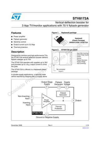
  • 1. November 2008 Rev 4 1/19 1 STV8172A Vertical deflection booster for 3 App TV/monitor applications with 70 V flyback generator Features ■ Power amplifier ■ Flyback generator ■ Stand-by control ■ Output current up to 3.0 App ■ Thermal protection Description Designed for monitors and high performance TVs, the STV8172A vertical deflection booster delivers flyback voltages up to 70V. The STV8172A operates with supplies up to 35V and provides up to 3 APP output current to drive the yoke. The STV8172A is offered in a Heptawatt plastic package. In double-supply applications, a stand-by state will be reached by stopping the (+) supply alone. Figure 1. Heptawatt package Figure 2. STV8172A pin detail Heptawatt (Plastic Package) ORDER CODE: STV8172A 7 6 5 4 3 2 1 Tab connected Input (Non Inverting) Output Stage Supply Output Ground Flyback Generator Supply Voltage Input (Inverting) to pin 4 7 Thermal Protection 6 4 3 5 STV8172A + - Power Amplifier 1 Flyback Generator Non-Inverting Inverting Input Input Ground or Negative Supply Output Flyback Generator Output Stage Supply VoltageSupply 2 www.st.com Obsolete Product(s) - Obsolete Product(s)
  • 2. Contents STV8172A 2/19 Contents 1 Absolute maximum ratings . . . . . . . . . . . . . . . . . . . . . . . . . . . . . . . . . . . 3 2 Thermal data . . . . . . . . . . . . . . . . . . . . . . . . . . . . . . . . . . . . . . . . . . . . . . . 4 3 Electrical characteristics . . . . . . . . . . . . . . . . . . . . . . . . . . . . . . . . . . . . . 5 4 Application hints . . . . . . . . . . . . . . . . . . . . . . . . . . . . . . . . . . . . . . . . . . . . 7 4.1 DC-coupled application . . . . . . . . . . . . . . . . . . . . . . . . . . . . . . . . . . . . . . . 7 4.1.1 Application hints . . . . . . . . . . . . . . . . . . . . . . . . . . . . . . . . . . . . . . . . . . . . 8 4.1.2 Ripple rejection . . . . . . . . . . . . . . . . . . . . . . . . . . . . . . . . . . . . . . . . . . . . 9 4.2 AC-coupled applications . . . . . . . . . . . . . . . . . . . . . . . . . . . . . . . . . . . . . . 10 4.2.1 Application hints . . . . . . . . . . . . . . . . . . . . . . . . . . . . . . . . . . . . . . . . . . . 10 4.3 Application with differential-output drivers . . . . . . . . . . . . . . . . . . . . . . . . 11 4.3.1 Centering . . . . . . . . . . . . . . . . . . . . . . . . . . . . . . . . . . . . . . . . . . . . . . . . 12 4.3.2 Peak current . . . . . . . . . . . . . . . . . . . . . . . . . . . . . . . . . . . . . . . . . . . . . . 12 4.3.3 Ripple rejection . . . . . . . . . . . . . . . . . . . . . . . . . . . . . . . . . . . . . . . . . . . 12 4.3.4 Secondary breakdown diagrams . . . . . . . . . . . . . . . . . . . . . . . . . . . . . . 13 5 Mounting instructions . . . . . . . . . . . . . . . . . . . . . . . . . . . . . . . . . . . . . . . 14 6 Pin configuration . . . . . . . . . . . . . . . . . . . . . . . . . . . . . . . . . . . . . . . . . . . 15 7 Package mechanical data . . . . . . . . . . . . . . . . . . . . . . . . . . . . . . . . . . . . 16 7.1 Lead-free packaging . . . . . . . . . . . . . . . . . . . . . . . . . . . . . . . . . . . . . . . . . 17 8 Revision history . . . . . . . . . . . . . . . . . . . . . . . . . . . . . . . . . . . . . . . . . . . 18 Obsolete Product(s) - Obsolete Product(s)
  • 3. STV8172A Absolute maximum ratings 3/19 1 Absolute maximum ratings Note: 1 Usually the flyback voltage is slightly more than 2 x VS. This must be taken into consideration when setting VS. 2 Versus pin 4 3 V3 is higher than VS during the first half of the flyback pulse. 4 Such repetitive output peak currents are usually observed just before and after the flyback pulse. 5 This non-repetitive output peak current can be observed, for example, during the Switch- On/Switch-Off phases. This peak current is acceptable providing the SOA is respected (Figure 10 and Figure 11). 6 All pins have a reverse diode towards pin 4, these diodes should never be forward-biased. 7 Input voltages must not exceed the lower value of either VS + 2 or 40 volts. Table 1. Absolute maximum ratings Symbol Parameter Value Unit Voltage VS Supply voltage (pin 2) - Note 1 and Note 2 40 V V5, V6 Flyback peak voltage - Note 2 70 V V3 Voltage at Pin 3 - Note 2, Note 3 and Note 6 -0.4 to (VS + 3) V V1, V7 Amplifier input voltage - Note 2, Note 6 and Note 7 - 0.4 to (VS + 2) or +40 V Current I0 (1) Output peak current at f = 50 to 200 Hz, t ≤10µs - Note 4 ±5 A I0 (2) Output peak current non-repetitive - Note 5 ±2 A I3 Sink Sink current, t<1ms - Note 3 2 A I3 Source Source current, t < 1ms 2 A I3 Flyback pulse current at f=50 to 200 Hz, t≤10μs - Note 4 ±5 A ESD Susceptibility ESD1 Human body model (100 pF discharged through 1.5 kΩ) 2 kV ESD2 EIAJ standard (200 pF discharged through 0 Ω) 300 V Temperature Ts Storage temperature -40 to 150 °C Tj Junction temperature +150 °C Obsolete Product(s) - Obsolete Product(s)
  • 4. Thermal data STV8172A 4/19 2 Thermal data Table 2. Thermal data Symbol Parameter Value Unit RthJC Junction-to-case thermal resistance 3 °C/W TT Temperature for thermal shutdown 150 °C TJ Recommended max. junction temperature 120 °C Obsolete Product(s) - Obsolete Product(s)
  • 5. STV8172A Electrical characteristics 5/19 3 Electrical characteristics VS = 34 V, TAMB = 25°C, unless otherwise specified. Table 3. Electrical characteristics Symbol Parameter Test Conditions Min. Typ. Max. Unit Figure Supply VS Operating supply voltage range (V2-V4) See note below(1) 10 35 V I2 Pin 2 quiescent current I3 = 0, I5 = 0 5 20 mA Figure 3 I6 Pin 6 quiescent current I3 = 0, I5 = 0, V6 =35v 8 19 50 mA Figure 3 Input I1 Input bias current V1 = 1 V, V7 = 2.2 V - 0.6 -1.5 µA Figure 3 I7 Input bias current V1 = 2.2 V, V7 = 1 V - 0.6 -1.5 µA VIR Operating input voltage range 0 VS - 2 V VI0 Offset voltage 2 mV ΔVI0/dt Offset drift versus temperature 10 µV/°C Output I0 Operating peak output current 0o <Tcase<125o C ±1.25 A V5L Output saturation voltage to pin 4 I5 = 1.25 A 0.9 1.6 V Figure 5 V5H Output saturation voltage to pin 6 I5 = -1.25 A 1.5 2.2 V Figure 4 Standby V5STBY Output voltage in standby V1 = V7 = Vs = 0(2) Figure 6 Miscellaneous G Voltage gain 80 dB VD5-6 Diode forward voltage between pins 5-6 I5 = 1.25 A 1.5 2.1 V VD3-2 Diode forward voltage between pins 3-2 I3 = 1.25 A 1.5 2.1 V V3SL Saturation voltage on pin 3 I3 = 20 mA 0.4 1 V Figure 5 V3SH Saturation voltage to pin 2 (2nd part of flyback) I3 = -1.25 A 1.8 2.6 V 1. In normal applications, the peak flyback voltage is slightly greater than 2 x (VS - V4). Therefore, (VS - V4) = 35 V is not allowed without special circuitry. 2. Refer to Figure 6, standby condition. Obsolete Product(s) - Obsolete Product(s)
  • 6. Electrical characteristics STV8172A 6/19 Figure 3. Measurement of I1, I2 and I6 Figure 4. Measurement of V5H Figure 5. Measurement of V3L and V5L 1V (a) 39kΩ 5 1 (b) I1 (a): I2 and I6 measurement (b): I1 measurement S +Vs 2 6 I2 I6 4 7 2.2V STV8172A 5.6kΩ - I5 5 1V 7 2.2V 1 4 +Vs 2 6 V5H STV8172A +Vs I3 or I5 3 5 V5L V3L (a)(b) (a): V5L measurement (b): V3L measurement STV8172A 1V 7 4 2 6 2.2V 1 Obsolete Product(s) - Obsolete Product(s)
  • 7. STV8172A Application hints 7/19 4 Application hints The yoke can be coupled either in AC or DC. 4.1 DC-coupled application When DC coupled (see Figure 6), the display vertical position can be adjusted with input bias. On the other hand, 2 supply sources (VS and -VEE) are required. A standby state will be reached by switching OFF the positive supply alone. In this state, where both inputs are the same voltage as pin 2 or higher, the output will sink negligible current from the deviation coil. Figure 6. DC-coupled application R3 +Vs R2 R1 Rd(*) Yoke Ly Vertical Position Adjustment -VEE Vref (*) recommended: Ly 50μs ------------- Rd Ly 20μs -------------<< 0.1µF 0.1µF CF (47 to 100µF) Power Amplifier Flyback Generator Thermal Safety 470µF 470µF Output Current Output Voltage Ip 7 3 2 5 6 1 4 VM Vm + - 0.22µF 1.5Ω Obsolete Product(s) - Obsolete Product(s)
  • 8. Application hints STV8172A 8/19 4.1.1 Application hints For calculations, treat the IC as an op-amp, where the feedback loop maintains V1 = V7. Centering Display will be centered (null mean current in yoke) when voltage on pin 7 is (R1 is negligible): Peak current Example: for Vm = 2 V, VM = 5 V and IP = 1 A Choose R1 in the1 Ω range, for instance R1=1 Ω From equation of peak current: Then choose R2 or R3. For instance, if R2 = 10 kΩ, then R3 = 15 kΩ Finally, the bias voltage on pin 7 should be: V7 V M V m + 2 ------------------------ R 2 R2 R3+ ---------------------- ⎝ ⎠ ⎜ ⎟ ⎛ ⎞ ×= I P V M V m –( ) 2 ----------------------------- R 2 R1xR3 -------------------×= R2 R3 ------- 2 IP R1×× VM Vm– ------------------------------- 2 3 ---== V7 VM Vm+ 2 ------------------------ 1 1 R3 R 2 -------+ -----------------× 7 2 ---- 1 2.5 --------× 1.4V=== Obsolete Product(s) - Obsolete Product(s)
  • 9. STV8172A Application hints 9/19 4.1.2 Ripple rejection When both ramp signal and bias are provided by the same driver IC, you can gain natural rejection of any ripple caused by a voltage drop in the ground (see Figure 7), if you manage to apply the same fraction of ripple voltage to both booster inputs. For that purpose, arrange an intermediate point in the bias resistor bridge, such that (R8 / R7) = (R3 / R2), and connect the bias filtering capacitor between the intermediate point and the local driver ground. Of course, R7 should be connected to the booster reference point, which is the ground side of R1. Figure 7. Ripple rejection R3 R2 R1 Rd Yoke Ly Power Amplifier Flyback Generator Thermal Safety 7 3 2 5 6 1 4 + - R7 R8R9 Reference Voltage Ramp Signal Driver Ground Source of Ripple Obsolete Product(s) - Obsolete Product(s)
  • 10. Application hints STV8172A 10/19 4.2 AC-coupled applications In AC-coupled applications (see Figure 8), only one supply (VS) is needed. The vertical position of the scanning cannot be adjusted with input bias (for that purpose, usually some current is injected or sunk with a resistor in the low side of the yoke). Figure 8. AC-coupled application 4.2.1 Application hints Gain is defined as in the previous case: Choose R1 then either R2 or R3. For good output centering, V7 must fulfill the following equation: R3 +Vs R2 R1 Rd(*) Yoke Ly (*) recommended: Ly 50μs ------------- Rd Ly 20μs -------------<< 0.1µF CF (47 to 100µF) Power Amplifier Flyback Generator Thermal Safety 470µF Output Current Output Voltage Ip 7 3 2 5 6 1 4 VM Vm + - Cs R4 CL R5 0.22µF 1.5Ω I p VM Vm– 2 ------------------------ R2 R1 R3× -----------------------×= VS 2 -------- V7– R4 R5+ ---------------------- V7 VM Vm+ 2 ------------------------– R3 -------------------------------------- V 7 R2 -------+= Obsolete Product(s) - Obsolete Product(s)
  • 11. STV8172A Application hints 11/19 or CS performs an integration of the parabolic signal on CL, therefore the amount of S correction is set by the combination of CL and Cs. 4.3 Application with differential-output drivers Certain driver ICs provide the ramp signal in differential form, as two current sources i+ and i−with opposite variations. Figure 9. Using a differential-output driver Some definitions: ● icm is the common-mode current: ● at peak of signal, i+ = icm + ip and i−= icm - ip, therefore the peak differential signal is ip - (-ip) = 2 ip, and the peak-peak differential signal, 4ip. The application is described in Figure 9 with DC yoke coupling. The calculations still rely on the fact that V1 remains equal to V7. V7 1 R3 ------- ⎝ ⎛ 1 R2 -------+× 1 R4 R5+ ---------------------- ⎠ ⎞ VS 2 R4 R5+( ) ------------------------------ VM Vm+ 2 R3× ------------------------+ ⎝ ⎠ ⎜ ⎟ ⎛ ⎞ =+ +Vs R2 R1 Rd(*) Yoke Ly -VEE 0.22µF (*) recommended: Ly 50μs ------------- Rd Ly 20μs -------------<< 0.1µF 0.1µF CF (47 to 100µF) Power Amplifier Flyback Generator Thermal Safety + - 470µF 470µF Output Current Output Voltage Ip 7 3 2 5 6 1 4 R7 + - Differential output driver IC ip icm -ipicm 1.5Ω icm 1 2 --- i+ i-+( )= Obsolete Product(s) - Obsolete Product(s)
  • 12. Application hints STV8172A 12/19 4.3.1 Centering When idle, both driver outputs provide icm and the yoke current should be null (R1 is negligible), hence: 4.3.2 Peak current Scanning current should be IP when positive and negative driver outputs provide respectively icm - ip and icm + ip, therefore Choose R1 in the 1Ω range, the value of R2 = R7 follows. Remember that i is one-quarter of driver peak-peak differential signal! Also check that the voltages on the driver outputs remain inside allowed range. Example: for icm = 0.4mA, i = 0.2mA (corresponding to 0.8mA of peak-peak differential current), Ip = 1A Choose R1 = 0.75Ω, it follows R2 = R7 = 1.875kΩ. 4.3.3 Ripple rejection Make sure to connect R7 directly to the ground side of R1. icm R7⋅ icm R2 therefore R7 R2=⋅= icm i–( ) R7⋅ Ip R1⋅ icm i+( ) R2⋅+= Ip i ----- 2R7 R1 -----------–= and since R7 = R2 Obsolete Product(s) - Obsolete Product(s)
  • 13. STV8172A Application hints 13/19 4.3.4 Secondary breakdown diagrams Figure 10. Output transistor safe operating area (SOA) for secondary breakdown The diagram has been arbitrarily limited to max I0 (2A). Figure 11. Secondary breakdown temperature derating curve (ISB = secondary breakdown current) Obsolete Product(s) - Obsolete Product(s)
  • 14. Mounting instructions STV8172A 14/19 5 Mounting instructions The power dissipated in the circuit is removed by adding an external heatsink. With the Heptawatt package, the heatsink is simply attached with a screw or a compression spring (clip). A layer of silicon grease inserted between heatsink and package optimizes thermal contact. In DC-coupled applications we recommend to use a silicone tape between the device tab and the heatsink to electrically isolate the tab. Figure 12. Mounting examples Obsolete Product(s) - Obsolete Product(s)
  • 15. STV8172A Pin configuration 15/19 6 Pin configuration Figure 13. Pins 1 and 7 Figure 14. Pins 3, 5 and 6 1 7 2 3 2 6 5 4 2 Obsolete Product(s) - Obsolete Product(s)
  • 16. Package mechanical data STV8172A 16/19 7 Package mechanical data Figure 15. 7-pin Heptawatt package A L L1 C D1 L5 L2 L3 D E M1 M H3 Dia. L7 L11 L10 L6 H2 F G G1 G2 E1 F E L9 V4 L4 H2 Table 4. Heptawatt package Dim. mm inches Min. Typ. Max. Min. Typ. Max. A 4.8 0.189 C 1.37 0.054 D 2.40 2.80 0.094 0.110 D1 1.20 1.35 0.047 0.053 E 0.35 0.55 0.014 0.022 E1 0.70 0.97 0.028 0.038 F 0.60 0.80 0.024 0.031 Obsolete Product(s) - Obsolete Product(s)
  • 17. STV8172A Package mechanical data 17/19 7.1 Lead-free packaging To meet environmental requirements, ST offers these devices in ECOPACK® packages. These packages have a lead-free second level interconnect. The category of second level interconnect is marked on the package and on the inner box label, in compliance with JEDEC Standard JESD97. The maximum ratings related to soldering conditions are also marked on the inner box label. ECOPACK is an ST trademark. ECOPACK specifications are available at: www.st.com. G 2.34 2.54 2.74 0.095 0.100 0.105 G1 4.88 5.08 5.28 0.193 0.200 0.205 G2 7.42 7.62 7.82 0.295 0.300 0.307 H2 10.40 0.409 H3 10.05 10.40 0.396 0.409 L 16.70 16.90 17.10 0.657 0.668 0.673 L1 14.92 0.587 L2 21.24 21.54 21.84 0.386 0.848 0.860 L3 22.27 22.52 22.77 0.877 0.891 0.896 L4 1.29 0.051 L5 2.60 2.80 3.00 0.102 0.110 0.118 L6 15.10 15.50 15.80 0.594 0.610 0.622 L7 6.00 6.35 6.60 0.0236 0.250 0.260 L9 0.20 0.008 L10 2.10 2.70 0.082 0.106 L11 4.30 4.80 0.169 0.190 M 2.55 2.80 3.05 0.100 0.110 0.120 M1 4.83 5.08 5.33 0.190 0.200 0.210 V4 40 (Typ.) Dia. 3.65 3.85 0.144 0.152 Table 4. Heptawatt package (continued) Dim. mm inches Obsolete Product(s) - Obsolete Product(s)
  • 18. Revision history STV8172A 18/19 8 Revision history Table 5. Document revision history Date Revision Changes August 2003 1 First issue. November 2003 1.1 Datasheet status changed to preliminary data. December 2003 1.2 Modification to Figure 13. June 2004 1.3 Datasheet status changed to datasheet. February 2005 2 Updated Figure 9. March 2005 3 Status changed to datasheet. 13-Nov-2008 4 Section 7.1 added, new template applied. Obsolete Product(s) - Obsolete Product(s)
  • 19. STV8172A 19/19 Please Read Carefully: Information in this document is provided solely in connection with ST products. STMicroelectronics NV and its subsidiaries (“ST”) reserve the right to make changes, corrections, modifications or improvements, to this document, and the products and services described herein at any time, without notice. All ST products are sold pursuant to ST’s terms and conditions of sale. Purchasers are solely responsible for the choice, selection and use of the ST products and services described herein, and ST assumes no liability whatsoever relating to the choice, selection or use of the ST products and services described herein. No license, express or implied, by estoppel or otherwise, to any intellectual property rights is granted under this document. If any part of this document refers to any third party products or services it shall not be deemed a license grant by ST for the use of such third party products or services, or any intellectual property contained therein or considered as a warranty covering the use in any manner whatsoever of such third party products or services or any intellectual property contained therein. UNLESS OTHERWISE SET FORTH IN ST’S TERMS AND CONDITIONS OF SALE ST DISCLAIMS ANY EXPRESS OR IMPLIED WARRANTY WITH RESPECT TO THE USE AND/OR SALE OF ST PRODUCTS INCLUDING WITHOUT LIMITATION IMPLIED WARRANTIES OF MERCHANTABILITY, FITNESS FOR A PARTICULAR PURPOSE (AND THEIR EQUIVALENTS UNDER THE LAWS OF ANY JURISDICTION), OR INFRINGEMENT OF ANY PATENT, COPYRIGHT OR OTHER INTELLECTUAL PROPERTY RIGHT. UNLESS EXPRESSLY APPROVED IN WRITING BY AN AUTHORIZED ST REPRESENTATIVE, ST PRODUCTS ARE NOT RECOMMENDED, AUTHORIZED OR WARRANTED FOR USE IN MILITARY, AIR CRAFT, SPACE, LIFE SAVING, OR LIFE SUSTAINING APPLICATIONS, NOR IN PRODUCTS OR SYSTEMS WHERE FAILURE OR MALFUNCTION MAY RESULT IN PERSONAL INJURY, DEATH, OR SEVERE PROPERTY OR ENVIRONMENTAL DAMAGE. ST PRODUCTS WHICH ARE NOT SPECIFIED AS "AUTOMOTIVE GRADE" MAY ONLY BE USED IN AUTOMOTIVE APPLICATIONS AT USER’S OWN RISK. Resale of ST products with provisions different from the statements and/or technical features set forth in this document shall immediately void any warranty granted by ST for the ST product or service described herein and shall not create or extend in any manner whatsoever, any liability of ST. ST and the ST logo are trademarks or registered trademarks of ST in various countries. Information in this document supersedes and replaces all information previously supplied. The ST logo is a registered trademark of STMicroelectronics. All other names are the property of their respective owners. © 2008 STMicroelectronics - All rights reserved STMicroelectronics group of companies Australia - Belgium - Brazil - Canada - China - Czech Republic - Finland - France - Germany - Hong Kong - India - Israel - Italy - Japan - Malaysia - Malta - Morocco - Singapore - Spain - Sweden - Switzerland - United Kingdom - United States of America www.st.com Obsolete Product(s) - Obsolete Product(s)