Fostering Friendships - Enhancing Social Bonds in the Classroom
Central processing unit
1. CENTRAL PROCESSING UNIT
INTRODUCTION
The part of the computer that performs the bulk of data-processing operations is called the central
processing unit and is referred to as the CPU.
The CPU is made up of three major parts1. The register set stores intermediate data used during the execution of the instructions.
2. The arithmetic logic unit (ALU) performs the required microoperations for executing the instructions.
3. The control unit supervises the transfer of information among the registers and instructs the ALU as to
which operation to perform.
The CPU performs a variety of functions dictated by the type of instructions that are incorporated in the
computer.
GENERAL REGISTER ORGANIZATION
In a simple multiplication, memory locations are needed for storing pointers, counters, return addresses,
temporary results, and partial products.
2. Having to refer to memory locations for such applications is time consuming because memory access is the
most time-consuming operation in a computer.
It is more convenient and more efficient to store these intermediate values in processor registers.
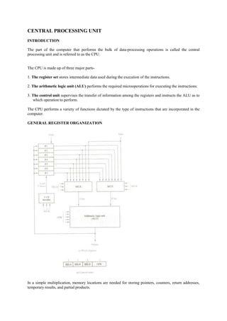
A bus organization for seven CPU registers is shown in Fig. 5-2.
The output of each register is connected to two multiplexers (MUX) to form the two buses A and B. The A
and B buses form the inputs to a common arithmetic logic unit (ALU). The operation selected in the ALU
determines the arithmetic or logic microoperation that is to be performed. The result of the microoperation
is available for output data and also goes into the inputs of all the registers. The register that receives the
information from the output bus is selected by a decoder.
For example, to perform the operation.
R1 ← R2 + R3
the control must provide binary selection variables to the following selector inputs:
1. MUX A selector (SELA): to place the content of R2 into bus A.
2. MUX B selector (SELB): to place the content of R3 into bus B.
3. ALU operation selector (OPR): to provide the arithmetic addition A + B.
4. Decoder destination selector (SELD): to transfer the content of the output bus into R1.
CONTROL WORD
There are 14 binary selection inputs in the unit, and their combined value specifies a control word.
The 14-bit control word consists of four fields. Three fields contain three bits each, and one field has five
bits. The three bits of SELA select a source register for the A input of the ALU. The three bits of SELB
select a register for the B input of the ALU. The three bits of SELD select a destination register using the
decoder and its seven load output. The five bits of OPR select one of the operations in the ALU.
3. EXAMPLE OF MICRO OPERATIONS
The control word for a given microoperation can be derived from the selection variables. For example, the
subtract microoperation given by the statement.
R1 ← R2 − R3
specifies R2 for the A input of the ALU, R3 for the B input of the ALU, R1 for the destination register, and
an ALU operation to subtract A − B.
The binary control word for the subtract microoperation is 010 011 001 00101 and is obtained as follows :
STACK ORGANIZATION
The stack in digital computers is essentially a memory unit with an address register that can count only.
The register that holds the address for the stack is called a stack pointer (SP) because its value always
points at the top item in the stack.
The two operations of a stack are the insertion and deletion of items. The operation of insertion is called
push (or push-down) because it can be through of as the result of pushing a new item on top. The operation
of deletion is called pop (or pop-up) because it can be thought of as the result of removing one item so that
the stack pops up. However, nothing is pushed or popped in a computer stack. these operation are
simulated by incrementing or decrementing the stack pointer register.
REGISTER STACK
A stack can be placed in portion of a large memory or it can be organized as a collection of a
finite number of memory words or registers. the organization of a 64-word
register stack.
4. The stack pointer register SP contains a binary number whose value is equal to the address of the word that
is currently on top of the stack. Three items are placed in the stack: A, B, and C, in that order. Item C is on
top of the stack so that the content of SP is now 3. To remove the top item, the stack is popped by reading
the memory word at address 3 and decrementing the content of SP. Item B is now on top the stack since SP
holds address 2.
In a 64-word stack, the stack pointer contains 6 bits because 26 = 64. Since SP has only six bits, it cannot
exceed a number greater than 63 (111111 in binary). When 63 is incremented by 1, the result is 0 since
111111 + 1 = 1000000 in binary, but SP can accommodate only the six least significant bits.
The one bits register FULL is set to 1 when the stack is full, and the one-bit register EMTY is set to 1
when the stack is empty of items. DR is the data register that holds the binary data to be written into or
read out of the stack. .
Initially, SP is cleared to 0, EMTY is set to 1, and FULL is cleared to 0, so that SP points to the word at
address 0 and the stack is marked empty and not full. If the stack is not full (if FULL = 0), a new item is
inserted with a push operation.
The push operation is implemented with the following sequence of microoperations:
SP ← SP + 1
Increment stack pointer
M [SP] ← DR Write item on top of the stack
If (SP = 0) then (FULL ← 1)
Check if stack is full
EMTY ← 0
Mark the stack not empty
A new item is deleted from the stack if the stack is not empty (if EMTY = 0). The pop operation consists
of the following sequence of microoperations:
DR ← M [SP] Read item from the top of stack
SP ← SP – 1 Decrement stack pointer
If (SP = 0) then (EMTY ← 1)
Check if stack is empty
FULL ← 0
Mark the stack not full
MEMORY STACK
5. computer memory partitioned into three segments: program, data, and stack.
The program counter PC points at the address of the next instruction in the program. The address register
AR points at an array of data. The stack pointer SP points at the top of the stack.
The three registers are connected to a common address bus, and either one can provide an address for
memory. PC is used during the fetch phase to read an instruction. AR is used during the execute phase to
read an operand. SP is used to push or pop items into or from the stack
the initial value of SP is 4001 and the stack grows with decreasing addresses. Thus the first item stored in
the stack is at address 4000, the second item is stored at address 3999, and the last address that can be used
for the stack is 3000. No provisions are available for stack limit checks.
We assume that the items in the stack communicate with a data register DR. A new item is inserted with
the push operation as follow:
6. SP ← SP – 1
M [SP] ← DR
The stack pointer is decremented so that it points at the address of the next word. A memory write
operation inserts the word form DR into the top of the stack. A new item is deleted with a pop operation as
follows:
DR ← M[SP]
SP ← SP + 1
The top is read form the stack into DR. The stack pointer is then incremented to point at the next item in
the stack.
INSTRUCTION FORMATS
A computer will usually have a variety of instruction code formats. It is the function of the control unit
within the CPU to interpret each instruction code and provide the necessary control functions needed to
process the instruction.
The format of an instruction is usually depicted in a rectangular box symbolizing the bits of the instruction
as they appear in memory words or in a control register. The bits of the instruction are divided into groups
called fields. The most common fields found in instruction formats are:
1. An operation code field that specifies the operation to be performed.
2. An address field that designates a memory address or a processor register.
3. A mode field that specifies the way the operand or the effective address is determined.
The operation code field of an instruction is a group of bits that define various processor operations, such
as add, subtract, complement, and shift.
The bits that define the mode field of an instruction code specify a variety of alternatives for choosing the
operands from the given address.
Computers may have instructions of several different lengths containing varying number of addresses. The
number of address fields in the instruction format of a computer depends on the internal organization of its
registers. Most computers fall into one of three types of CPU organizations:
1. Single accumulator organization.
2. General register organization.
3. Stack organization.
an accumulator-type organization is the basic computer All operations are performed with an implied
accumulator register. The instruction format in this type of computer uses one address field. For example,
the instruction that specifies an arithmetic addition is defined by an assembly language instruction as
ADD X where X is the address of the operand. The ADD instruction in this case results in the operation
AC ← AC + M[X]. AC is the accumulator register and M[X] symbolizes the memory word located at
address X.
An example of a general register type of organization was presented in Fig. 7.1. The instruction format in
this type of computer needs three register address fields. Thus the instruction for an arithmetic addition
may be written in an assembly language as ADD R1, R2, R3 to denote the operation R1 ← R2 + R3. The
number of address fields in the instruction can be reduced from three to two if the destination register is the
same as one of the source registers.
Thus the instruction
ADD R1, R2
would denote the operation R1 ← R1 + R2.
7. General register-type computers employ two or three address fields in their instruction format. Each
address field may specify a processor register or a memory word. An instruction symbolized by ADD R1,
X would specify the operation R1 ← R + M [X]. It has two address fields, one for register R1 and the
other for the memory address X.
Computers with stack organization would have PUSH and POP instructions which require an address field.
Thus the instruction
PUSH X
will push the word at address X to the top of the stack. The stack pointer is updated automatically.
Operation-type instructions do not need an address field in stack-organized computers. This is because the
operation is performed on the two items that are on top of the stack. The instruction ADD in a stack
computer consists of an operation code only with no address field. This operation has the effect of popping
the two top numbers from the stack, adding the numbers, and pushing the sum into the stack.
To illustrate the influence of the number of addresses on computer programs, we will evaluate the
arithmetic statement
X = (A + B) ∗ (C + D)
using zero, one, two, or three address instruction.
THREE-ADDRESS INSTRUCTIONS
Computers with three-address instruction formats can use each address field to specify either a processor
register or a memory operand. The program in assembly language that evaluates X = (A + B) ∗ (C + D) is
shown below, together with comments that explain the register transfer operation of each instruction.
ADD R1, A, B R1 ← M [A] + M [B]
ADD R2, C, D R2 ← M [C] + M [D]
MUL X, R1, R2 M [X] ← R1 ∗ R2
The advantage of the three-address format is that it results in short programs when evaluating arithmetic
expressions. The disadvantage is that the binary-coded instructions require too many bits to specify three
addresses.
TWO-ADDRESS INSTRUCTIONS
Two address instructions are the most common in commercial computers. Here again each address field
can specify either a processor register or a memory word. The program to evaluate X = (A + B) ∗ (C + D)
is as follows:
MOV R1, A R1 ← M [A]
ADD R1, B R1 ← R1 + M [B]
MOV R2, C R2 ← M [C]
ADD R2, D R2 ← R2 + M [D]
MUL R1, R2 R1 ← R1 ∗ R2
MOV X, R1 M [X] ← R1
ONE-ADDRESS INSTRUCTIONS
One-address instructions use an implied accumulator (AC) register for all data manipulation. For
multiplication and division there is a need for a second register. However, here we will neglect the second
and assume that the AC contains the result of tall operations. The program to evaluate X = (A + B) ∗ (C +
D) is
LOAD A
8. AC ← M [A]
ADD B AC ← A [C] + M [B]
STORE T M [T] ← AC
LOAD C AC ← M [C]
ADD D AC ← AC + M [D]
MUL T AC ← AC ∗ M [T]
STORE X M [X] ← AC
All operation are done between the AC register and a memory operand. T is the address of a temporary
memory location required for storing the intermediate result
ZERO-ADDRESS INSTRUCTIONS
A stack-organized computer does not use an address field for the instructions ADD and MUL. The PUSH
and POP instructions, however, need an address field to specify the operand that communicates with the
stack. The following program shows how X = (A + B) ∗ (C + D) will be written for a stack organized
computer. (TOS stands for top of stack)
PUSH A TOS ← A
PUSH B TOS ← B
ADD TOS ← (A + B)
PUSH C TOS ← C
PUSH D TOS ← D
ADD TOS ← (C + D)
MUL TOS ← (C + D) ∗ (A + B)
POP X M [X] ← TOS
To evaluate arithmetic expressions in a stack computer, it is necessary to convert the expression into
reverse Polish notation. The name “zero-address” is given to this type of computer because of the absence
of an address field in the computational instructions
RISC INSTRUCTIONS
The reduced instruction set computer (RISC) architecture have several advantages. The instruction set of a
typical of a typical RISC processor is restricted to the use of load and store instructions when
communicating between memory and CPU.
All other instruction are executed within the registers of the CPU without referring to memory. A program
for a RISC-type CPU consists of LOAD and STORE instructions that have one memory and one register
address, and computational-type instructions that have three addresses with all three specifying processor
registers.
The following is a program to evaluate X = (A + B) ∗ (C + D).
LOAD R1, A R1 ← M [A]
LOAD R2, B R2 ← M [B]
LOAD R3, C R3 ← M [C]
LOAD R4, D R4 ← M [D]
ADD R1, R1, R2 R1 ← R1 + R2
ADD R3, R3, R4 R3 ← R3 + R4
MUL R1, R1, R3 R1 ← R1 ∗ R3
STORE X, R1 M [X] ← R1
ADDRESSING MODES
9. Although most addressing modes modify the address field of the instruction, there are two modes that need
no address field at all. These are the implied and immediate modes.
Implied Mode:
In this mode the operands are specified implicitly in the definition of the instruction. For example, the
instruction “complement accumulator” is an implied-mode instruction because the operand in the
accumulator register is implied in the definition of the instruction. In fact, all register reference instructions
that sue an accumulator are implied-mode instructions.
Zero-address instructions in a stack-organized computer are implied-mode instructions since the operands
are implied to be on top of the stack.
Immediate Mode : In this mode the operand is specified in the instruction itself. In other words, an
immediate-mode instruction has an operand field rather than an address field. Immediate-mode instructions
are useful for initializing registers to a constant value.
It was mentioned previously that the address field of an instruction may specify either a memory word or a
processor register. When the address field specifies a processor register, the instruction is said to be in the
register mode.
5.5.3 Register Mode :
In this mode the operands are in registers that reside within the CPU. The particular register is selected
from a register field in the instruction. A k-bit field can specify any one of 2k registers.
5.5.4 Register Indirect Mode :
In this mode the instruction specifies a register in the CPU whose contents give the address of the operand
in memory. In other words, the selected register contains the address of the operand rather than the operand
itself.
Autoincrement or Autodecrement Mode
This is similar to the register indirect mode except that the register is incremented or decremented after (or
before) its value is used to access memory.
Direct Address Mode:
In this mode the effective address is equal to the address part of the instruction. The operand resides in
memory and its address is given directly by the address field of the instruction.
Indirect Address Mode:
In this mode the address field of the instruction gives the address where the effective address is stored in
memory. Control fetches the instruction from memory and uses its address part to access memory again to
read the effective address.
Relative Address Mode:
In this mode the content of the program counter is added to the address part of the instruction in order to
obtain the effective address.
The address part of the instruction is usually a signed number (in 2’s complement representation) which
can be either positive or negative. When this number is added to the content of the program counter, the
result produces an effective address whose position in memory is relative to the address of the next
10. instruction.
Indexed Addressing Mode:
In this mode the content of an index register is added to the address part of the instruction to obtain the
effective address. The index register is a special CPU register that contains an index value. The address
field of the instruction defines the beginning address of a data array in memory. Each operand in the array
is stored in memory relative to the beginning address. The distance between the beginning address and the
address of the operand is the index value stores in the index register.
Base Register Addressing Mode:
In this mode the content of a base register is added to the address part of the instruction to obtain the
effective address. This is similar to the indexed addressing mode except that the register is now called a
base register instead of an index register.