SlideShare una empresa de Scribd logo
1 de 9
Descargar para leer sin conexión
MOTOROLA                                                                                                               Order this document
 SEMICONDUCTOR TECHNICAL DATA                                                                                                by MPX4100/D


                                                                                                             MPX4100

 Integrated Silicon Pressure Sensor                                                                            SERIES

 Manifold Absolute Pressure Sensor
 On-Chip Signal Conditioned,
                                                                                                                 INTEGRATED
 Temperature Compensated                                                                                    PRESSURE SENSOR
                                                                                                        20 to 105 kPa (2.9 to 15.2 psi)
 and Calibrated                                                                                               0.3 to 4.9 V Output
   The Motorola MPX4100 series Manifold Absolute Pressure (MAP) sensor for engine
 control is designed to sense absolute air pressure within the intake manifold. This
 measurement can be used to compute the amount of fuel required for each cylinder. The
 small form factor and high reliability of on–chip integration makes the Motorola MAP
 sensor a logical and economical choice for automotive system designers.
 Features
 • 1.8% Maximum Error Over 0° to 85°C
 • Specifically Designed for Intake Manifold Absolute Pressure Sensing in Engine
   Control Systems
 • Ideally Suited for Microprocessor Interfacing                                                             BASIC CHIP CARRIER
 • Patented Silicon Shear Stress Strain Gauge                                                                     ELEMENT
                                                                                                             CASE 867–08, STYLE 1
 • Temperature Compensated Over – 40°C to +125°C
 • Durable Epoxy Unibody Element
 • Ideal for Non–Automotive Applications                                                                         PIN NUMBER
 Application Examples                                                                                    1       Vout        4       N/C
 • Manifold Sensing for Automotive Systems                                                               2       Gnd         5       N/C
                                                                                                         3        VS         6       N/C
                                                                                                       NOTE: Pins 4, 5, and 6 are internal
                                                                                                       device connections. Do not connect
                                                                                                       to external circuitry or ground. Pin 1
                                                                                                       is noted by the notch in the Lead.
                          VS

                            3

                                                                              The MPX4100 series piezoresistive transducer is a state–
                                                                           of–the–art, monolithic, signal conditioned, silicon pressure
                         THIN FILM        GAIN STAGE #2                    sensor. This sensor, with its patented transducer, combines
       X–ducer         TEMPERATURE             AND
      SENSING          COMPENSATION          GROUND
                                                              1            advanced micromachining techniques, thin film metallization,
                                                                    Vout
      ELEMENT               AND            REFERENCE                       and bipolar semiconductor processing to provide an
                       GAIN STAGE #1     SHIFT CIRCUITRY                   accurate, high level analog output signal that is proportional
                                                                           to applied pressure.
                   2                                                          Figure 1 shows a block diagram of the internal circuitry in-
                                  PINS 4, 5 AND 6 ARE NO CONNECTS
                                                                           tegrated on a pressure sensor chip.
                 GND

  Figure 1. Fully Integrated Pressure Sensor Schematic


 Senseon and X–ducer are trademarks of Motorola, Inc.


 REV 3

  Motorola Sensor Device Data                                                                                                              1
© Motorola, Inc. 1997
MPX4100 SERIES
MAXIMUM RATINGS(1)
                             Parametric                                       Symbol                         Value                     Unit
  Overpressure(2) (P1 > P2)                                                        Pmax                         400                    kPa
  Burst Pressure(2) (P1 > P2)                                                  Pburst                        1000                      kPa
  Storage Temperature                                                              Tstg                   – 40 to +125                  °C
  Operating Temperature                                                             TA                    – 40 to +125                  °C
1. TC = 25°C unless otherwise noted.
2. Exposure beyond the specified limits may cause permanent damage or degradation to the device.


OPERATING CHARACTERISTICS (VS = 5.1 Vdc, TA = 25°C unless otherwise noted, P1 > P2)
                            Characteristic                                  Symbol          Min            Typ           Max            Unit
  Pressure Range(1)                                                          POP             20             —            105            kPa
  Supply Voltage(1)                                                           VS            4.85           5.1           5.35           Vdc
  Supply Current                                                               Io            —             7.0            10           mAdc
  Minimum Pressure Offset(3)               (0 to 85°C)                        Voff         0.225          0.306          0.388          Vdc
    @ VS = 5.1 Volts
  Full Scale Output(4)                     (0 to 85°C)                       VFSO          4.815          4.897          4.978          Vdc
    @ VS = 5.1 Volts
  Full Scale Span(5)                       (0 to 85°C)                       VFSS            —             4.59           —             Vdc
    @ VS = 5.1 Volts
  Accuracy(6)                              (0 to 85°C)                         —             —              —            ±1.8         %VFSS
  Sensitivity                                                                 V/P            —             54             —           mV/kPa
  Response Time(7)                                                             tR            —             1.0            —             ms
  Output Source Current at Full Scale Output                                  Io+            —             0.1            —            mAdc
  Warm–Up Time(8)                                                              —             —             20             —             ms
  Offset Stability(9)                                                          —             —            ± 0.5           —           %VFSS
Decoupling circuit shown in Figure 3 required to meet electrical specifications.


MECHANICAL CHARACTERISTICS
                            Characteristic                                  Symbol          Min            Typ           Max            Unit
  Weight, Basic Element (Case 867)                                             —             —             4.0            —           Grams
  Common Mode Line Pressure(10)                                                —             —              —            690            kPa
NOTES:
  1. 1.0 kPa (kiloPascal) equals 0.145 psi.
  2. Device is ratiometric within this specified excitation range.
  3. Offset (Voff) is defined as the output voltage at the minimum rated pressure.
  4. Full Scale Output (VFSO) is defined as the output voltage at the maximum or full rated pressure.
  5. Full Scale Span (VFSS) is defined as the algebraic difference between the output voltage at full rated pressure and the output voltage at the
     minimum rated pressure.
  6. Accuracy (error budget) consists of the following:
    • Linearity:                     Output deviation from a straight line relationship with pressure over the specified pressure range.
    • Temperature Hysteresis: Output deviation at any temperature within the operating temperature range, after the temperature is
                                     cycled to and from the minimum or maximum operating temperature points, with zero differential pressure
                                     applied.
    • Pressure Hysteresis:           Output deviation at any pressure within the specified range, when this pressure is cycled to and from the
                                     minimum or maximum rated pressure, at 25°C.
    • TcSpan:                        Output deviation over the temperature range of 0 to 85°C, relative to 25°C.
    • TcOffset:                      Output deviation with minimum rated pressure applied, over the temperature range of 0 to 85°C, relative to
                                     25°C.
    • Variation from Nominal: The variation from nominal values, for Offset or Full Scale Span, as a percent of VFSS, at 25°C.
  7. Response Time is defined as the time for the incremental change in the output to go from 10% to 90% of its final value when subjected to
     a specified step change in pressure.
  8. Warm–up is defined as the time required for the product to meet the specified output voltage after the Pressure has been stabilized.
  9. Offset stability is the product’s output deviation when subjected to 1000 hours of Pulsed Pressure, Temperature Cycling with Bias Test.
 10. Common mode pressures beyond specified may result in leakage at the case–to–lead interface.


  2                                                                                                              Motorola Sensor Device Data
MPX4100 SERIES
        FLUORO SILICONE                                                                         SENSOR
          GEL DIE COAT                                     STAINLESS                                                           A/D
                                                                                                OUTPUT
                            DIE                            STEEL CAP
                                                                                                 (PIN 1)
                                  P1                                      EPOXY
                                                                         PLASTIC                         50 pF       51 k
 WIRE BOND ÉÉÉÉÉÉÉÉÉÉÉ
           ÉÉÉÉÉÉÉÉÉÉÉ                                                     CASE                                                   µ PROCESSOR


           ÉÉÉÉÉÉÉÉÉÉÉ
    LEAD
   FRAME
           ÉÉÉÉÉÉÉÉÉÉÉABSOLUTE ELEMENT
                                                                        DIE
                                                                       BOND
 SEALED VACUUM REFERENCE    P2

             Figure 2. Cross Sectional Diagram                                                        Figure 3. Decoupling Filter for Sensor to
                        (Not to Scale)                                                                       Microprocessor Interface


   Figure 2 illustrates an absolute sensing chip in the basic                              Figure 3 shows a typical decoupling circuit for interfacing
chip carrier (Case 867). A fluorosilicone gel isolates the die                           the integrated MAP sensor to the A/D input of a microproces-
surface and wire bonds from the environment, while allowing                              sor. Proper decoupilng of the power supply is recommended.
the pressure signal to be transmitted to the sensor dia-                                   Figure 4 shows the sensor output signal relative to pres-
phragm. The MPX4100A series pressure sensor operating                                    sure input. Typical, minimum, and maximum output curves
characteristics, and internal reliability and qualification tests                        are shown for operation over a temperature range of 0° to
are based on use of dry air as the pressure media. Media,                                85°C. (The output will saturate outside of the specified pres-
other than dry air, may have adverse effects on sensor                                   sure range.)
performance and long–term reliability. Contact the factory for
information regarding media compatibility in your application.


                                                    5.0
                                                    4.5   TRANSFER FUNCTION:                    MAX
                                                          Vout = Vs* (.01059*P–.152) ± Error
                                                    4.0
                                                          VS = 5.1 Vdc
                                                                                                                  TYP
                                                    3.5   TEMP = 0 to 85°C
                                   OUTPUT (Volts)


                                                          20 kPa TO 105 kPa
                                                    3.0
                                                          MPX4100A
                                                    2.5
                                                    2.0
                                                    1.5
                                                                                         MIN
                                                    1.0
                                                    0.5
                                                     0
                                                           5

                                                          15

                                                          25

                                                          35

                                                          45

                                                          55
                                                          60
                                                          65

                                                          75

                                                          85

                                                          95
                                                         100
                                                         105
                                                         110
                                                          10

                                                          20

                                                          30

                                                          40

                                                          50


                                                          70

                                                          80

                                                          90


                                                                       Pressure (ref: to sealed vacuum) in kPa

                                                            Figure 4. Output versus Absolute Pressure


 Motorola Sensor Device Data                                                                                                                       3
MPX4100 SERIES
       Transfer Function (MPX4100A)
     Nominal Transfer Value: Vout = VS (P x 0.01059 – 0.1518)
                             +/– (Pressure Error x Temp. Factor x 0.01059 x VS)
                             VS = 5.1 V ± 0.25 Vdc


       Temperature Error Band
                                                                  MPX4100A Series


                                              4.0

                                                                               Temp                 Multiplier
                                              3.0
                                                                               – 40                 3
            Temperature                                                        0 to 85              1
                                              2.0                              +125                 3
               Error
              Factor
                                              1.0


                                              0.0
                                                     –40   –20    0          20          40        60      80       100       120        140

                                                                                       Temperature in C°


       Pressure Error Band


                                              3.0                     Error Limits for Pressure

                                              2.0
                      Pressure Error (kPa)


                                              1.0

                                              0.0                                                                                 Pressure (in kPa)
                                                             20       40          60          80    100      120
                                             –1.0

                                             – 2.0

                                             – 3.0
                                                                                                                Pressure            Error (Max)
                                                                                                                20 to 105 (kPa)     ± 1.5 (kPa)


 4                                                                                                                                  Motorola Sensor Device Data
MPX4100 SERIES
                            PRESSURE (P1)/VACUUM (P2) SIDE IDENTIFICATION TABLE

  Motorola designates the two sides of the pressure sensor         pressure sensor is designed to operate with positive differen-
as the Pressure (P1) side and the Vacuum (P2) side. The            tial pressure applied, P1 > P2.
Pressure (P1) side is the side containing fluorosilicone gel          The Pressure (P1) side may be identified by using the table
which protects the die from harsh media. The Motorola MPX          below:


                                                                                                  Pressure (P1)
                  Part Number                         Case Type                                   Side Identifier
 MPX4100A                                              867–08               Stainless Steel Cap
 MPX4100AP                                             867B–04              Side with Port Marking
 MPX4100AS                                             867E–03              Side with Port Attached
 MPX4100ASX                                            867F–03              Side with Port Attached


ORDERING INFORMATION
  The MPX4100A series MAP silicon pressure sensors are available in the Basic Element, or with pressure port fittings that
provide mounting ease and barbed hose connections.
                                                                                                   MPX Series
    Device Type
    D i T                         Options
                                  O i                    Case Type
                                                         C    T                 Order Number                    Device Marking
 Basic Element          Absolute, Element Only            867–08            MPX4100A                       MPX4100A
 Ported Elements        Absolute, Ported                  867B–04           MPX4100AP                      MPX4100AP
                        Absolute, Stove Pipe Port         867E–03           MPX4100AS                      MPX4100A
                        Absolute, Axial Port              867F–03           MPX4100ASX                     MPX4100A


 Motorola Sensor Device Data                                                                                                     5
MPX4100 SERIES
                                                                        PACKAGE DIMENSIONS


                       C                                                                                                                                              NOTES:
                                                                                                                                                                        1. DIMENSIONING AND TOLERANCING PER ANSI
                                                                                            R                                                                              Y14.5M, 1982.
                                                                                                                                                                        2. CONTROLLING DIMENSION: INCH.
                                                                                                                              POSITIVE PRESSURE
                                                                                                                              (P1)                                      3. DIMENSION –A– IS INCLUSIVE OF THE MOLD
                               M                                                                                                                                           STOP RING. MOLD STOP RING NOT TO EXCEED
                                                                                                                                                                           16.00 (0.630).

              B                     –A–                                                                                                                                               INCHES         MILLIMETERS
                                                                                                                                                                           DIM     MIN     MAX        MIN     MAX
                                                                                                                                                                            A     0.595    0.630     15.11    16.00
                                                                                                                            N                                               B     0.514    0.534     13.06    13.56
                                                         PIN 1
                                                                                                                                  L                                         C     0.200    0.220      5.08     5.59
                                                                        1       2       3       4       5       6
                                                  SEATING                                                                                                                   D     0.027    0.033      0.68     0.84
                                                  PLANE
                                                             –T–                                                                                                            F     0.048    0.064      1.22     1.63
                                                                                                                                                                            G       0.100 BSC           2.54 BSC
                                                                                                                                                                            J     0.014    0.016      0.36     0.40
                 J                                                                                                      G                                                   L     0.695    0.725     17.65    18.42
                 S                                                  F                                                                                                       M        30 _NOM            30 _NOM
                                                                                                    D 6 PL                                                                  N     0.475    0.495     12.07    12.57
                                                                                                                                                                            R     0.430    0.450     10.92    11.43
                                                                                                                0.136 (0.005)         M    T A     M
                                                                                                                                                                            S     0.090    0.105      2.29     2.66

                                                                                                                                                                            STYLE 1:
                                                                                                                                                                              PIN 1.   VOUT
                                                                                                                                                                                  2.   GROUND
                                                                                                                                                                                  3.   VCC
                                                                                                                                                                                  4.   V1
                                                                                                                                                                                  5.   V2
                                                                                            CASE 867–08                                                                           6.   VEX
                                                                                              ISSUE N

                                                                         BASIC ELEMENT (A, D)


                                                                                                                                                                          NOTES:
                                                                                            A                                                                               1. DIMENSIONING AND TOLERANCING PER ANSI
             –T–     SEATING                                                                                                                                                   Y14.5M, 1982.
                     PLANE                                                                  U                                             PORT #1                           2. CONTROLLING DIMENSION: INCH.
                                                                                            L                                             POSITIVE
                                                                                                                                          PRESSURE (P1)                                    INCHES        MILLIMETERS
             R                                                                                                                                                                   DIM    MIN     MAX       MIN     MAX
                                                                                        V
                                                                                                                                                                                  A    1.145    1.175    29.08    29.85
                                                                                                                                                                                  B    0.685    0.715    17.40    18.16
                                                                                                                                            –Q–                                   C    0.305    0.325     7.75     8.26
                           N                                                                                                                                                      D    0.027    0.033     0.68     0.84
                                                                                                                                                                                  F    0.048    0.064     1.22     1.63
                                                                                                                                                                                  G      0.100 BSC          2.54 BSC
                                                                                                                                                                                  J    0.014    0.016     0.36     0.41
                                                                                                                                                                                  K    0.695    0.725    17.65    18.42
                                                   B                                                                                                                              L    0.290    0.300     7.37     7.62
                                                                                                                                                                                  N    0.420    0.440    10.67    11.18
                                                                                                                                                                                  P    0.153    0.159     3.89     4.04
                                                                                                                                                                                  Q    0.153    0.159     3.89     4.04
                                                                                                                                                   K                              R    0.230    0.250     5.84     6.35
                                                                            1       2       3       4       5       6
                                                                                                                                                                                  S    0.220    0.240     5.59     6.10
                                                            PIN 1                                                                          S                                      U      0.910 BSC         23.11 BSC
                                                                                                                                                                                  V    0.182    0.194     4.62     4.93
     C                                –P–
                                                                    G                                                       D 6 PL
                               0.25 (0.010)   M    T Q      M                                                                                                                    STYLE 1:
         J                                                                  F                                                  0.13 (0.005)    M   T P    S   Q   S                PIN 1.   VOUT
                                                                                                                                                                                       2.   GROUND
                                                                                                                                                                                       3.   VCC
                                                                                                                                                                                       4.   V1
                                                                                                                                                                                       5.   V2
                                                                                                                                                                                       6.   VEX
                                                                                        CASE 867B–04
                                                                                          ISSUE E

                                                                PRESSURE SIDE PORTED (AP, GP)


 6                                                                                                                                                                           Motorola Sensor Device Data
MPX4100 SERIES
                                                      PACKAGE DIMENSIONS—CONTINUED


                                                                                                                                               NOTES:
                              C                                                         A                                                        1. DIMENSIONING AND TOLERANCING PER ANSI
                                                                                                                                                    Y14.5M, 1982.
                                                                                                                                                 2. CONTROLLING DIMENSION: INCH.

                                                                                                                                                              INCHES       MILLIMETERS
                                                                                                                                                    DIM    MIN     MAX      MIN     MAX
                                                                                                                                                     A    0.690    0.720   17.53    18.28
      –B–     V                                                                                                                                      B    0.245    0.255    6.22     6.48
                                                                                                                                                     C    0.780    0.820   19.81    20.82
                                                                                                                        PIN 1
                                                                                                                                                     D    0.027    0.033    0.69     0.84
                                                                                                                                                     E    0.178    0.186    4.52     4.72
                                                                                                                                                     F    0.048    0.064    1.22     1.63
     PORT #1                                                               6    5   4       3   2       1                                            G      0.100 BSC         2.54 BSC
    POSITIVE                                                                                                                                         J    0.014    0.016    0.36     0.41
   PRESSURE
         (P1)                                         K                                                                                              K    0.345    0.375    8.76     9.53
                                                               S                                                                                     N    0.300    0.310    7.62     7.87
                                                                                                                                                     S    0.220    0.240    5.59     6.10
                                                                                                                                                     V    0.182    0.194    4.62     4.93
                                                  J                G
                                                                               F                                                                           STYLE 1:
                          N    E                                                                                D   6 PL                                     PIN 1.   VOUT
                                                                                                                                                                 2.   GROUND
                                    –T–                                                                         0.13 (0.005)    M       T B   M                  3.   VCC
                                                                                                                                                                 4.   V1
                                                                                                                                                                 5.   V2
                                                                                                                                                                 6.   VEX


                                                                               CASE 867E–03
                                                                                 ISSUE D

                                                           PRESSURE SIDE PORTED (AS, GS)


                              –T–
                  C                                                                         A                                                          NOTES:
                                                                                                                                                         1. DIMENSIONING AND TOLERANCING PER
                      E                                                                     U                                                 –Q–           ANSI Y14.5M, 1982.
                                                                                                                                                         2. CONTROLLING DIMENSION: INCH.

                                                                                                                                                                      INCHES       MILLIMETERS
                                                                                                                                                            DIM    MIN     MAX      MIN     MAX
                                                                                                                                                             A    1.080    1.120   27.43    28.45
                                                                                                                                                             B    0.740    0.760   18.80    19.30
                                                                                                                                                             C    0.630    0.650   16.00    16.51
                                                                                                                                    N
  V                                                                                                                                           B
                                                                                                                                                             D    0.027    0.033    0.68     0.84
                                                                                                                                                             E    0.160    0.180    4.06     4.57
                                                                                                                                                             F    0.048    0.064    1.22     1.63
                                                                                                                                         R                   G      0.100 BSC         2.54 BSC
                                                                                                                        PIN 1                                J    0.014    0.016    0.36     0.41
   PORT #1
  POSITIVE                                                                                                                                                   K    0.220    0.240    5.59     6.10
 PRESSURE                     –P–                                                                                                                            N    0.070    0.080    1.78     2.03
       (P1)                          0.25 (0.010)     M   T Q      M       6    5       4       3       2   1                                                P    0.150    0.160    3.81     4.06
                                                                                                                                    S                        Q    0.150    0.160    3.81     4.06
                                                                                                                                                             R    0.440    0.460   11.18    11.68
                                                                                                                    K                                        S    0.695    0.725   17.65    18.42
                                                                                                                                                             U    0.840    0.860   21.34    21.84
                                                                                                                                                             V    0.182    0.194    4.62     4.93
                  J                                             D 6 PL
                                                                                                    G
                               0.13 (0.005)   M     T P    S    Q S                                                                                         STYLE 1:
                                                                                                                                                              PIN 1.   VOUT
                                                                                                                                                                  2.   GROUND
                                                                       F                                                                                          3.   VCC
                                                                                                                                                                  4.   V1
                                                                                                                                                                  5.   V2
                                                                                                                                                                  6.   VEX

                                                                               CASE 867F–03
                                                                                 ISSUE D

                                                          PRESSURE SIDE PORTED (ASX, GSX)


Motorola Sensor Device Data                                                                                                                                                                         7
MPX4100 SERIES


Motorola reserves the right to make changes without further notice to any products herein. Motorola makes no warranty, representation or guarantee regarding
the suitability of its products for any particular purpose, nor does Motorola assume any liability arising out of the application or use of any product or circuit, and
specifically disclaims any and all liability, including without limitation consequential or incidental damages. “Typical” parameters which may be provided in Motorola
data sheets and/or specifications can and do vary in different applications and actual performance may vary over time. All operating parameters, including “Typicals”
must be validated for each customer application by customer’s technical experts. Motorola does not convey any license under its patent rights nor the rights of
others. Motorola products are not designed, intended, or authorized for use as components in systems intended for surgical implant into the body, or other
applications intended to support or sustain life, or for any other application in which the failure of the Motorola product could create a situation where personal injury
or death may occur. Should Buyer purchase or use Motorola products for any such unintended or unauthorized application, Buyer shall indemnify and hold Motorola
and its officers, employees, subsidiaries, affiliates, and distributors harmless against all claims, costs, damages, and expenses, and reasonable attorney fees
arising out of, directly or indirectly, any claim of personal injury or death associated with such unintended or unauthorized use, even if such claim alleges that
Motorola was negligent regarding the design or manufacture of the part. Motorola and               are registered trademarks of Motorola, Inc. Motorola, Inc. is an Equal
Opportunity/Affirmative Action Employer.
                                                                                                                                  Mfax is a trademark of Motorola, Inc.
How to reach us:
USA / EUROPE / Locations Not Listed: Motorola Literature Distribution;                 JAPAN: Nippon Motorola Ltd.; Tatsumi–SPD–JLDC, 6F Seibu–Butsuryu–Center,
P.O. Box 5405, Denver, Colorado 80217. 303–675–2140 or 1–800–441–2447                  3–14–2 Tatsumi Koto–Ku, Tokyo 135, Japan. 81–3–3521–8315

Mfax™: RMFAX0@email.sps.mot.com – TOUCHTONE 602–244–6609            ASIA/PACIFIC: Motorola Semiconductors H.K. Ltd.; 8B Tai Ping Industrial Park,
                                  – US & Canada ONLY 1–800–774–1848 51 Ting Kok Road, Tai Po, N.T., Hong Kong. 852–26629298
INTERNET: http://motorola.com/sps


 8                                                 ◊                                                                                                   MPX4100/D
                                                                                                                                  Motorola Sensor Device Data
This datasheet has been download from:

      www.datasheetcatalog.com

Datasheets for electronics components.

Más contenido relacionado

La actualidad más candente

Maitry Instruments & Control, Surat, Process Control Instruments
Maitry Instruments & Control, Surat, Process Control InstrumentsMaitry Instruments & Control, Surat, Process Control Instruments
Maitry Instruments & Control, Surat, Process Control InstrumentsIndiaMART InterMESH Limited
 
W-BAND RADIOMETER SYSTEM WITH SWITCHING FRONT-END FOR MULTI-LOAD CALIBRATION.pdf
W-BAND RADIOMETER SYSTEM WITH SWITCHING FRONT-END FOR MULTI-LOAD CALIBRATION.pdfW-BAND RADIOMETER SYSTEM WITH SWITCHING FRONT-END FOR MULTI-LOAD CALIBRATION.pdf
W-BAND RADIOMETER SYSTEM WITH SWITCHING FRONT-END FOR MULTI-LOAD CALIBRATION.pdfgrssieee
 
At Lab Dcc Dpi7 Only V0.4
At Lab Dcc Dpi7 Only  V0.4At Lab Dcc Dpi7 Only  V0.4
At Lab Dcc Dpi7 Only V0.4alanlai.wae
 
Sca1000 Fm A0%200 As
Sca1000 Fm A0%200 AsSca1000 Fm A0%200 As
Sca1000 Fm A0%200 Asguest987902e
 
MUSES8920の英語のデータシート
MUSES8920の英語のデータシートMUSES8920の英語のデータシート
MUSES8920の英語のデータシートspicepark
 
1 touch art home switches
1 touch art home switches1 touch art home switches
1 touch art home switchesnannu31
 
Sound Devices MixPre
Sound Devices MixPreSound Devices MixPre
Sound Devices MixPreAV ProfShop
 

La actualidad más candente (18)

2 page s40 data sheet
2 page s40 data sheet2 page s40 data sheet
2 page s40 data sheet
 
Maitry Instruments & Control, Surat, Process Control Instruments
Maitry Instruments & Control, Surat, Process Control InstrumentsMaitry Instruments & Control, Surat, Process Control Instruments
Maitry Instruments & Control, Surat, Process Control Instruments
 
Data sheet
Data sheetData sheet
Data sheet
 
W-BAND RADIOMETER SYSTEM WITH SWITCHING FRONT-END FOR MULTI-LOAD CALIBRATION.pdf
W-BAND RADIOMETER SYSTEM WITH SWITCHING FRONT-END FOR MULTI-LOAD CALIBRATION.pdfW-BAND RADIOMETER SYSTEM WITH SWITCHING FRONT-END FOR MULTI-LOAD CALIBRATION.pdf
W-BAND RADIOMETER SYSTEM WITH SWITCHING FRONT-END FOR MULTI-LOAD CALIBRATION.pdf
 
At Lab Dcc Dpi7 Only V0.4
At Lab Dcc Dpi7 Only  V0.4At Lab Dcc Dpi7 Only  V0.4
At Lab Dcc Dpi7 Only V0.4
 
Sca1000 Fm A0%200 As
Sca1000 Fm A0%200 AsSca1000 Fm A0%200 As
Sca1000 Fm A0%200 As
 
Lpc662
Lpc662Lpc662
Lpc662
 
Sfp(ft 9001 g-m-lc02)-datasheet_ver_1.1
Sfp(ft 9001 g-m-lc02)-datasheet_ver_1.1Sfp(ft 9001 g-m-lc02)-datasheet_ver_1.1
Sfp(ft 9001 g-m-lc02)-datasheet_ver_1.1
 
Eclipse manual
Eclipse manualEclipse manual
Eclipse manual
 
SFP(FT-901A-M-LC02)_DataSheet_ver_1_2
SFP(FT-901A-M-LC02)_DataSheet_ver_1_2SFP(FT-901A-M-LC02)_DataSheet_ver_1_2
SFP(FT-901A-M-LC02)_DataSheet_ver_1_2
 
MUSES8920の英語のデータシート
MUSES8920の英語のデータシートMUSES8920の英語のデータシート
MUSES8920の英語のデータシート
 
Transistor BLF578
Transistor BLF578 Transistor BLF578
Transistor BLF578
 
2 n60
2 n602 n60
2 n60
 
SFP(FT-901B-M-LC02)_DataSheet_ver_1.1
SFP(FT-901B-M-LC02)_DataSheet_ver_1.1SFP(FT-901B-M-LC02)_DataSheet_ver_1.1
SFP(FT-901B-M-LC02)_DataSheet_ver_1.1
 
Cd4047
Cd4047Cd4047
Cd4047
 
1 touch art home switches
1 touch art home switches1 touch art home switches
1 touch art home switches
 
2
22
2
 
Sound Devices MixPre
Sound Devices MixPreSound Devices MixPre
Sound Devices MixPre
 

Similar a D1 be29c1d01

NM310S Product Brochure: Nonlinear Starter Kit For Agilent VNA
NM310S Product Brochure: Nonlinear Starter Kit For Agilent VNANM310S Product Brochure: Nonlinear Starter Kit For Agilent VNA
NM310S Product Brochure: Nonlinear Starter Kit For Agilent VNANMDG NV
 
PNAPlus Product Brochure: Nonlinear Starter Kit For Agilent VNA
PNAPlus Product Brochure: Nonlinear Starter Kit For Agilent VNAPNAPlus Product Brochure: Nonlinear Starter Kit For Agilent VNA
PNAPlus Product Brochure: Nonlinear Starter Kit For Agilent VNANMDG NV
 
ZVxPlus Product Brochure: Nonlinear Starter Kit For R&S VNA
ZVxPlus Product Brochure: Nonlinear Starter Kit For R&S VNAZVxPlus Product Brochure: Nonlinear Starter Kit For R&S VNA
ZVxPlus Product Brochure: Nonlinear Starter Kit For R&S VNANMDG NV
 
NM310S Product Brochure: Nonlinear Starter Kit For R&S VNA
NM310S Product Brochure: Nonlinear Starter Kit For R&S VNANM310S Product Brochure: Nonlinear Starter Kit For R&S VNA
NM310S Product Brochure: Nonlinear Starter Kit For R&S VNANMDG NV
 
Datasheet sensor temperatura mcp9700
Datasheet sensor temperatura mcp9700Datasheet sensor temperatura mcp9700
Datasheet sensor temperatura mcp9700ADELIUS
 
Product solution_compressed.pdf
Product solution_compressed.pdfProduct solution_compressed.pdf
Product solution_compressed.pdfesenhawer
 
Rsf ms 2x_series_catalog
Rsf ms 2x_series_catalogRsf ms 2x_series_catalog
Rsf ms 2x_series_catalogElectromate
 
Digital potentiometer ds1804 010+
Digital potentiometer ds1804 010+Digital potentiometer ds1804 010+
Digital potentiometer ds1804 010+robertoestrella
 
R38 Controller
R38 ControllerR38 Controller
R38 ControllerJoseph
 
Gu641 B Genset Control Operation Manual[1]
Gu641 B Genset Control Operation Manual[1]Gu641 B Genset Control Operation Manual[1]
Gu641 B Genset Control Operation Manual[1]ALEXIS BECERRA
 

Similar a D1 be29c1d01 (20)

Lm6171
Lm6171Lm6171
Lm6171
 
NM310S Product Brochure: Nonlinear Starter Kit For Agilent VNA
NM310S Product Brochure: Nonlinear Starter Kit For Agilent VNANM310S Product Brochure: Nonlinear Starter Kit For Agilent VNA
NM310S Product Brochure: Nonlinear Starter Kit For Agilent VNA
 
PNAPlus Product Brochure: Nonlinear Starter Kit For Agilent VNA
PNAPlus Product Brochure: Nonlinear Starter Kit For Agilent VNAPNAPlus Product Brochure: Nonlinear Starter Kit For Agilent VNA
PNAPlus Product Brochure: Nonlinear Starter Kit For Agilent VNA
 
ZVxPlus Product Brochure: Nonlinear Starter Kit For R&S VNA
ZVxPlus Product Brochure: Nonlinear Starter Kit For R&S VNAZVxPlus Product Brochure: Nonlinear Starter Kit For R&S VNA
ZVxPlus Product Brochure: Nonlinear Starter Kit For R&S VNA
 
NM310S Product Brochure: Nonlinear Starter Kit For R&S VNA
NM310S Product Brochure: Nonlinear Starter Kit For R&S VNANM310S Product Brochure: Nonlinear Starter Kit For R&S VNA
NM310S Product Brochure: Nonlinear Starter Kit For R&S VNA
 
Mt8880 Pk77
Mt8880 Pk77Mt8880 Pk77
Mt8880 Pk77
 
Datasheet sensor temperatura mcp9700
Datasheet sensor temperatura mcp9700Datasheet sensor temperatura mcp9700
Datasheet sensor temperatura mcp9700
 
great adc
great adcgreat adc
great adc
 
Product solution_compressed.pdf
Product solution_compressed.pdfProduct solution_compressed.pdf
Product solution_compressed.pdf
 
Capacitance Continuous Level Transmitter.pdf
Capacitance Continuous Level Transmitter.pdfCapacitance Continuous Level Transmitter.pdf
Capacitance Continuous Level Transmitter.pdf
 
Ads7843
Ads7843Ads7843
Ads7843
 
Capacitance Type Level Switch Manufacturers in Indiia
Capacitance Type Level Switch Manufacturers in IndiiaCapacitance Type Level Switch Manufacturers in Indiia
Capacitance Type Level Switch Manufacturers in Indiia
 
Rsf ms 2x_series_catalog
Rsf ms 2x_series_catalogRsf ms 2x_series_catalog
Rsf ms 2x_series_catalog
 
Acs712 datasheet
Acs712 datasheetAcs712 datasheet
Acs712 datasheet
 
Digital potentiometer ds1804 010+
Digital potentiometer ds1804 010+Digital potentiometer ds1804 010+
Digital potentiometer ds1804 010+
 
R38 Controller
R38 ControllerR38 Controller
R38 Controller
 
PG Pressure Sensor Brochure
PG Pressure Sensor BrochurePG Pressure Sensor Brochure
PG Pressure Sensor Brochure
 
lm3914.pdf
lm3914.pdflm3914.pdf
lm3914.pdf
 
Acs712 sensor-arus
Acs712 sensor-arusAcs712 sensor-arus
Acs712 sensor-arus
 
Gu641 B Genset Control Operation Manual[1]
Gu641 B Genset Control Operation Manual[1]Gu641 B Genset Control Operation Manual[1]
Gu641 B Genset Control Operation Manual[1]
 

D1 be29c1d01

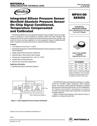
  • 1. MOTOROLA Order this document SEMICONDUCTOR TECHNICAL DATA by MPX4100/D MPX4100 Integrated Silicon Pressure Sensor SERIES Manifold Absolute Pressure Sensor On-Chip Signal Conditioned, INTEGRATED Temperature Compensated PRESSURE SENSOR 20 to 105 kPa (2.9 to 15.2 psi) and Calibrated 0.3 to 4.9 V Output The Motorola MPX4100 series Manifold Absolute Pressure (MAP) sensor for engine control is designed to sense absolute air pressure within the intake manifold. This measurement can be used to compute the amount of fuel required for each cylinder. The small form factor and high reliability of on–chip integration makes the Motorola MAP sensor a logical and economical choice for automotive system designers. Features • 1.8% Maximum Error Over 0° to 85°C • Specifically Designed for Intake Manifold Absolute Pressure Sensing in Engine Control Systems • Ideally Suited for Microprocessor Interfacing BASIC CHIP CARRIER • Patented Silicon Shear Stress Strain Gauge ELEMENT CASE 867–08, STYLE 1 • Temperature Compensated Over – 40°C to +125°C • Durable Epoxy Unibody Element • Ideal for Non–Automotive Applications PIN NUMBER Application Examples 1 Vout 4 N/C • Manifold Sensing for Automotive Systems 2 Gnd 5 N/C 3 VS 6 N/C NOTE: Pins 4, 5, and 6 are internal device connections. Do not connect to external circuitry or ground. Pin 1 is noted by the notch in the Lead. VS 3 The MPX4100 series piezoresistive transducer is a state– of–the–art, monolithic, signal conditioned, silicon pressure THIN FILM GAIN STAGE #2 sensor. This sensor, with its patented transducer, combines X–ducer TEMPERATURE AND SENSING COMPENSATION GROUND 1 advanced micromachining techniques, thin film metallization, Vout ELEMENT AND REFERENCE and bipolar semiconductor processing to provide an GAIN STAGE #1 SHIFT CIRCUITRY accurate, high level analog output signal that is proportional to applied pressure. 2 Figure 1 shows a block diagram of the internal circuitry in- PINS 4, 5 AND 6 ARE NO CONNECTS tegrated on a pressure sensor chip. GND Figure 1. Fully Integrated Pressure Sensor Schematic Senseon and X–ducer are trademarks of Motorola, Inc. REV 3 Motorola Sensor Device Data 1 © Motorola, Inc. 1997
  • 2. MPX4100 SERIES MAXIMUM RATINGS(1) Parametric Symbol Value Unit Overpressure(2) (P1 > P2) Pmax 400 kPa Burst Pressure(2) (P1 > P2) Pburst 1000 kPa Storage Temperature Tstg – 40 to +125 °C Operating Temperature TA – 40 to +125 °C 1. TC = 25°C unless otherwise noted. 2. Exposure beyond the specified limits may cause permanent damage or degradation to the device. OPERATING CHARACTERISTICS (VS = 5.1 Vdc, TA = 25°C unless otherwise noted, P1 > P2) Characteristic Symbol Min Typ Max Unit Pressure Range(1) POP 20 — 105 kPa Supply Voltage(1) VS 4.85 5.1 5.35 Vdc Supply Current Io — 7.0 10 mAdc Minimum Pressure Offset(3) (0 to 85°C) Voff 0.225 0.306 0.388 Vdc @ VS = 5.1 Volts Full Scale Output(4) (0 to 85°C) VFSO 4.815 4.897 4.978 Vdc @ VS = 5.1 Volts Full Scale Span(5) (0 to 85°C) VFSS — 4.59 — Vdc @ VS = 5.1 Volts Accuracy(6) (0 to 85°C) — — — ±1.8 %VFSS Sensitivity V/P — 54 — mV/kPa Response Time(7) tR — 1.0 — ms Output Source Current at Full Scale Output Io+ — 0.1 — mAdc Warm–Up Time(8) — — 20 — ms Offset Stability(9) — — ± 0.5 — %VFSS Decoupling circuit shown in Figure 3 required to meet electrical specifications. MECHANICAL CHARACTERISTICS Characteristic Symbol Min Typ Max Unit Weight, Basic Element (Case 867) — — 4.0 — Grams Common Mode Line Pressure(10) — — — 690 kPa NOTES: 1. 1.0 kPa (kiloPascal) equals 0.145 psi. 2. Device is ratiometric within this specified excitation range. 3. Offset (Voff) is defined as the output voltage at the minimum rated pressure. 4. Full Scale Output (VFSO) is defined as the output voltage at the maximum or full rated pressure. 5. Full Scale Span (VFSS) is defined as the algebraic difference between the output voltage at full rated pressure and the output voltage at the minimum rated pressure. 6. Accuracy (error budget) consists of the following: • Linearity: Output deviation from a straight line relationship with pressure over the specified pressure range. • Temperature Hysteresis: Output deviation at any temperature within the operating temperature range, after the temperature is cycled to and from the minimum or maximum operating temperature points, with zero differential pressure applied. • Pressure Hysteresis: Output deviation at any pressure within the specified range, when this pressure is cycled to and from the minimum or maximum rated pressure, at 25°C. • TcSpan: Output deviation over the temperature range of 0 to 85°C, relative to 25°C. • TcOffset: Output deviation with minimum rated pressure applied, over the temperature range of 0 to 85°C, relative to 25°C. • Variation from Nominal: The variation from nominal values, for Offset or Full Scale Span, as a percent of VFSS, at 25°C. 7. Response Time is defined as the time for the incremental change in the output to go from 10% to 90% of its final value when subjected to a specified step change in pressure. 8. Warm–up is defined as the time required for the product to meet the specified output voltage after the Pressure has been stabilized. 9. Offset stability is the product’s output deviation when subjected to 1000 hours of Pulsed Pressure, Temperature Cycling with Bias Test. 10. Common mode pressures beyond specified may result in leakage at the case–to–lead interface. 2 Motorola Sensor Device Data
  • 3. MPX4100 SERIES FLUORO SILICONE SENSOR GEL DIE COAT STAINLESS A/D OUTPUT DIE STEEL CAP (PIN 1) P1 EPOXY PLASTIC 50 pF 51 k WIRE BOND ÉÉÉÉÉÉÉÉÉÉÉ ÉÉÉÉÉÉÉÉÉÉÉ CASE µ PROCESSOR ÉÉÉÉÉÉÉÉÉÉÉ LEAD FRAME ÉÉÉÉÉÉÉÉÉÉÉABSOLUTE ELEMENT DIE BOND SEALED VACUUM REFERENCE P2 Figure 2. Cross Sectional Diagram Figure 3. Decoupling Filter for Sensor to (Not to Scale) Microprocessor Interface Figure 2 illustrates an absolute sensing chip in the basic Figure 3 shows a typical decoupling circuit for interfacing chip carrier (Case 867). A fluorosilicone gel isolates the die the integrated MAP sensor to the A/D input of a microproces- surface and wire bonds from the environment, while allowing sor. Proper decoupilng of the power supply is recommended. the pressure signal to be transmitted to the sensor dia- Figure 4 shows the sensor output signal relative to pres- phragm. The MPX4100A series pressure sensor operating sure input. Typical, minimum, and maximum output curves characteristics, and internal reliability and qualification tests are shown for operation over a temperature range of 0° to are based on use of dry air as the pressure media. Media, 85°C. (The output will saturate outside of the specified pres- other than dry air, may have adverse effects on sensor sure range.) performance and long–term reliability. Contact the factory for information regarding media compatibility in your application. 5.0 4.5 TRANSFER FUNCTION: MAX Vout = Vs* (.01059*P–.152) ± Error 4.0 VS = 5.1 Vdc TYP 3.5 TEMP = 0 to 85°C OUTPUT (Volts) 20 kPa TO 105 kPa 3.0 MPX4100A 2.5 2.0 1.5 MIN 1.0 0.5 0 5 15 25 35 45 55 60 65 75 85 95 100 105 110 10 20 30 40 50 70 80 90 Pressure (ref: to sealed vacuum) in kPa Figure 4. Output versus Absolute Pressure Motorola Sensor Device Data 3
  • 4. MPX4100 SERIES Transfer Function (MPX4100A) Nominal Transfer Value: Vout = VS (P x 0.01059 – 0.1518) +/– (Pressure Error x Temp. Factor x 0.01059 x VS) VS = 5.1 V ± 0.25 Vdc Temperature Error Band MPX4100A Series 4.0 Temp Multiplier 3.0 – 40 3 Temperature 0 to 85 1 2.0 +125 3 Error Factor 1.0 0.0 –40 –20 0 20 40 60 80 100 120 140 Temperature in C° Pressure Error Band 3.0 Error Limits for Pressure 2.0 Pressure Error (kPa) 1.0 0.0 Pressure (in kPa) 20 40 60 80 100 120 –1.0 – 2.0 – 3.0 Pressure Error (Max) 20 to 105 (kPa) ± 1.5 (kPa) 4 Motorola Sensor Device Data
  • 5. MPX4100 SERIES PRESSURE (P1)/VACUUM (P2) SIDE IDENTIFICATION TABLE Motorola designates the two sides of the pressure sensor pressure sensor is designed to operate with positive differen- as the Pressure (P1) side and the Vacuum (P2) side. The tial pressure applied, P1 > P2. Pressure (P1) side is the side containing fluorosilicone gel The Pressure (P1) side may be identified by using the table which protects the die from harsh media. The Motorola MPX below: Pressure (P1) Part Number Case Type Side Identifier MPX4100A 867–08 Stainless Steel Cap MPX4100AP 867B–04 Side with Port Marking MPX4100AS 867E–03 Side with Port Attached MPX4100ASX 867F–03 Side with Port Attached ORDERING INFORMATION The MPX4100A series MAP silicon pressure sensors are available in the Basic Element, or with pressure port fittings that provide mounting ease and barbed hose connections. MPX Series Device Type D i T Options O i Case Type C T Order Number Device Marking Basic Element Absolute, Element Only 867–08 MPX4100A MPX4100A Ported Elements Absolute, Ported 867B–04 MPX4100AP MPX4100AP Absolute, Stove Pipe Port 867E–03 MPX4100AS MPX4100A Absolute, Axial Port 867F–03 MPX4100ASX MPX4100A Motorola Sensor Device Data 5
  • 6. MPX4100 SERIES PACKAGE DIMENSIONS C NOTES: 1. DIMENSIONING AND TOLERANCING PER ANSI R Y14.5M, 1982. 2. CONTROLLING DIMENSION: INCH. POSITIVE PRESSURE (P1) 3. DIMENSION –A– IS INCLUSIVE OF THE MOLD M STOP RING. MOLD STOP RING NOT TO EXCEED 16.00 (0.630). B –A– INCHES MILLIMETERS DIM MIN MAX MIN MAX A 0.595 0.630 15.11 16.00 N B 0.514 0.534 13.06 13.56 PIN 1 L C 0.200 0.220 5.08 5.59 1 2 3 4 5 6 SEATING D 0.027 0.033 0.68 0.84 PLANE –T– F 0.048 0.064 1.22 1.63 G 0.100 BSC 2.54 BSC J 0.014 0.016 0.36 0.40 J G L 0.695 0.725 17.65 18.42 S F M 30 _NOM 30 _NOM D 6 PL N 0.475 0.495 12.07 12.57 R 0.430 0.450 10.92 11.43 0.136 (0.005) M T A M S 0.090 0.105 2.29 2.66 STYLE 1: PIN 1. VOUT 2. GROUND 3. VCC 4. V1 5. V2 CASE 867–08 6. VEX ISSUE N BASIC ELEMENT (A, D) NOTES: A 1. DIMENSIONING AND TOLERANCING PER ANSI –T– SEATING Y14.5M, 1982. PLANE U PORT #1 2. CONTROLLING DIMENSION: INCH. L POSITIVE PRESSURE (P1) INCHES MILLIMETERS R DIM MIN MAX MIN MAX V A 1.145 1.175 29.08 29.85 B 0.685 0.715 17.40 18.16 –Q– C 0.305 0.325 7.75 8.26 N D 0.027 0.033 0.68 0.84 F 0.048 0.064 1.22 1.63 G 0.100 BSC 2.54 BSC J 0.014 0.016 0.36 0.41 K 0.695 0.725 17.65 18.42 B L 0.290 0.300 7.37 7.62 N 0.420 0.440 10.67 11.18 P 0.153 0.159 3.89 4.04 Q 0.153 0.159 3.89 4.04 K R 0.230 0.250 5.84 6.35 1 2 3 4 5 6 S 0.220 0.240 5.59 6.10 PIN 1 S U 0.910 BSC 23.11 BSC V 0.182 0.194 4.62 4.93 C –P– G D 6 PL 0.25 (0.010) M T Q M STYLE 1: J F 0.13 (0.005) M T P S Q S PIN 1. VOUT 2. GROUND 3. VCC 4. V1 5. V2 6. VEX CASE 867B–04 ISSUE E PRESSURE SIDE PORTED (AP, GP) 6 Motorola Sensor Device Data
  • 7. MPX4100 SERIES PACKAGE DIMENSIONS—CONTINUED NOTES: C A 1. DIMENSIONING AND TOLERANCING PER ANSI Y14.5M, 1982. 2. CONTROLLING DIMENSION: INCH. INCHES MILLIMETERS DIM MIN MAX MIN MAX A 0.690 0.720 17.53 18.28 –B– V B 0.245 0.255 6.22 6.48 C 0.780 0.820 19.81 20.82 PIN 1 D 0.027 0.033 0.69 0.84 E 0.178 0.186 4.52 4.72 F 0.048 0.064 1.22 1.63 PORT #1 6 5 4 3 2 1 G 0.100 BSC 2.54 BSC POSITIVE J 0.014 0.016 0.36 0.41 PRESSURE (P1) K K 0.345 0.375 8.76 9.53 S N 0.300 0.310 7.62 7.87 S 0.220 0.240 5.59 6.10 V 0.182 0.194 4.62 4.93 J G F STYLE 1: N E D 6 PL PIN 1. VOUT 2. GROUND –T– 0.13 (0.005) M T B M 3. VCC 4. V1 5. V2 6. VEX CASE 867E–03 ISSUE D PRESSURE SIDE PORTED (AS, GS) –T– C A NOTES: 1. DIMENSIONING AND TOLERANCING PER E U –Q– ANSI Y14.5M, 1982. 2. CONTROLLING DIMENSION: INCH. INCHES MILLIMETERS DIM MIN MAX MIN MAX A 1.080 1.120 27.43 28.45 B 0.740 0.760 18.80 19.30 C 0.630 0.650 16.00 16.51 N V B D 0.027 0.033 0.68 0.84 E 0.160 0.180 4.06 4.57 F 0.048 0.064 1.22 1.63 R G 0.100 BSC 2.54 BSC PIN 1 J 0.014 0.016 0.36 0.41 PORT #1 POSITIVE K 0.220 0.240 5.59 6.10 PRESSURE –P– N 0.070 0.080 1.78 2.03 (P1) 0.25 (0.010) M T Q M 6 5 4 3 2 1 P 0.150 0.160 3.81 4.06 S Q 0.150 0.160 3.81 4.06 R 0.440 0.460 11.18 11.68 K S 0.695 0.725 17.65 18.42 U 0.840 0.860 21.34 21.84 V 0.182 0.194 4.62 4.93 J D 6 PL G 0.13 (0.005) M T P S Q S STYLE 1: PIN 1. VOUT 2. GROUND F 3. VCC 4. V1 5. V2 6. VEX CASE 867F–03 ISSUE D PRESSURE SIDE PORTED (ASX, GSX) Motorola Sensor Device Data 7
  • 8. MPX4100 SERIES Motorola reserves the right to make changes without further notice to any products herein. Motorola makes no warranty, representation or guarantee regarding the suitability of its products for any particular purpose, nor does Motorola assume any liability arising out of the application or use of any product or circuit, and specifically disclaims any and all liability, including without limitation consequential or incidental damages. “Typical” parameters which may be provided in Motorola data sheets and/or specifications can and do vary in different applications and actual performance may vary over time. All operating parameters, including “Typicals” must be validated for each customer application by customer’s technical experts. Motorola does not convey any license under its patent rights nor the rights of others. Motorola products are not designed, intended, or authorized for use as components in systems intended for surgical implant into the body, or other applications intended to support or sustain life, or for any other application in which the failure of the Motorola product could create a situation where personal injury or death may occur. Should Buyer purchase or use Motorola products for any such unintended or unauthorized application, Buyer shall indemnify and hold Motorola and its officers, employees, subsidiaries, affiliates, and distributors harmless against all claims, costs, damages, and expenses, and reasonable attorney fees arising out of, directly or indirectly, any claim of personal injury or death associated with such unintended or unauthorized use, even if such claim alleges that Motorola was negligent regarding the design or manufacture of the part. Motorola and are registered trademarks of Motorola, Inc. Motorola, Inc. is an Equal Opportunity/Affirmative Action Employer. Mfax is a trademark of Motorola, Inc. How to reach us: USA / EUROPE / Locations Not Listed: Motorola Literature Distribution; JAPAN: Nippon Motorola Ltd.; Tatsumi–SPD–JLDC, 6F Seibu–Butsuryu–Center, P.O. Box 5405, Denver, Colorado 80217. 303–675–2140 or 1–800–441–2447 3–14–2 Tatsumi Koto–Ku, Tokyo 135, Japan. 81–3–3521–8315 Mfax™: RMFAX0@email.sps.mot.com – TOUCHTONE 602–244–6609 ASIA/PACIFIC: Motorola Semiconductors H.K. Ltd.; 8B Tai Ping Industrial Park, – US & Canada ONLY 1–800–774–1848 51 Ting Kok Road, Tai Po, N.T., Hong Kong. 852–26629298 INTERNET: http://motorola.com/sps 8 ◊ MPX4100/D Motorola Sensor Device Data
  • 9. This datasheet has been download from: www.datasheetcatalog.com Datasheets for electronics components.