
Recomendados
Más contenido relacionado
La actualidad más candente
Destacado
Destacado (8)
Similar a Datasheet
Similar a Datasheet (20)
Último
Último (20)
Datasheet
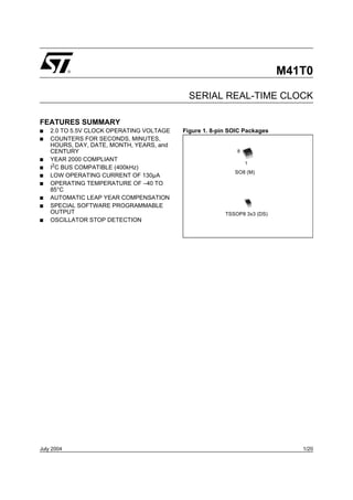
- 1. M41T0 SERIAL REAL-TIME CLOCK FEATURES SUMMARY ■ 2.0 TO 5.5V CLOCK OPERATING VOLTAGE Figure 1. 8-pin SOIC Packages ■ COUNTERS FOR SECONDS, MINUTES, HOURS, DAY, DATE, MONTH, YEARS, and CENTURY 8 ■ YEAR 2000 COMPLIANT 1 ■ I2C BUS COMPATIBLE (400kHz) SO8 (M) ■ LOW OPERATING CURRENT OF 130µA ■ OPERATING TEMPERATURE OF –40 TO 85°C ■ AUTOMATIC LEAP YEAR COMPENSATION ■ SPECIAL SOFTWARE PROGRAMMABLE OUTPUT TSSOP8 3x3 (DS) ■ OSCILLATOR STOP DETECTION July 2004 1/20
- 2. M41T0 TABLE OF CONTENTS FEATURES SUMMARY . . . . . . . . . . . . . . . . . . . . . . . . . . . . . . . . . . . . . . . . . . . . . . . . . . . . . . . . . . . . . 1 Figure 1. 8-pin SOIC Packages . . . . . . . . . . . . . . . . . . . . . . . . . . . . . . . . . . . . . . . . . . . . . . . . . . . . 1 SUMMARY DESCRIPTION . . . . . . . . . . . . . . . . . . . . . . . . . . . . . . . . . . . . . . . . . . . . . . . . . . . . . . . . . . . 4 Figure 2. Logic Diagram . . . . . . . . . . . . . . . . . . . . . . . . . . . . . . . . . . . . . . . . . . . . . . . . . . . . . . . . . . 4 Figure 3. SOIC Connections . . . . . . . . . . . . . . . . . . . . . . . . . . . . . . . . . . . . . . . . . . . . . . . . . . . . . . . 4 Table 1. Signal Names . . . . . . . . . . . . . . . . . . . . . . . . . . . . . . . . . . . . . . . . . . . . . . . . . . . . . . . . . . 4 Figure 4. Block Diagram . . . . . . . . . . . . . . . . . . . . . . . . . . . . . . . . . . . . . . . . . . . . . . . . . . . . . . . . . . 5 MAXIMUM RATING. . . . . . . . . . . . . . . . . . . . . . . . . . . . . . . . . . . . . . . . . . . . . . . . . . . . . . . . . . . . . . . . . 6 Table 2. Absolute Maximum Ratings . . . . . . . . . . . . . . . . . . . . . . . . . . . . . . . . . . . . . . . . . . . . . . . . 6 DC AND AC PARAMETERS. . . . . . . . . . . . . . . . . . . . . . . . . . . . . . . . . . . . . . . . . . . . . . . . . . . . . . . . . . 7 Table 3. Operating and AC Measurement Conditions . . . . . . . . . . . . . . . . . . . . . . . . . . . . . . . . . . . 7 Figure 5. AC Testing Input/Output Waveform. . . . . . . . . . . . . . . . . . . . . . . . . . . . . . . . . . . . . . . . . . 7 Table 4. Capacitance. . . . . . . . . . . . . . . . . . . . . . . . . . . . . . . . . . . . . . . . . . . . . . . . . . . . . . . . . . . . 7 Table 5. DC Characteristics. . . . . . . . . . . . . . . . . . . . . . . . . . . . . . . . . . . . . . . . . . . . . . . . . . . . . . . 8 Table 6. Crystal Electrical Characteristics . . . . . . . . . . . . . . . . . . . . . . . . . . . . . . . . . . . . . . . . . . . . 8 OPERATION . . . . . . . . . . . . . . . . . . . . . . . . . . . . . . . . . . . . . . . . . . . . . . . . . . . . . . . . . . . . . . . . . . . . . . 9 2-Wire Bus Characteristics . . . . . . . . . . . . . . . . . . . . . . . . . . . . . . . . . . . . . . . . . . . . . . . . . . . . . . . 9 Bus not busy.. . . . . . . . . . . . . . . . . . . . . . . . . . . . . . . . . . . . . . . . . . . . . . . . . . . . . . . . . . . . . . . . . . . 9 Start data transfer.. . . . . . . . . . . . . . . . . . . . . . . . . . . . . . . . . . . . . . . . . . . . . . . . . . . . . . . . . . . . . . . 9 Stop data transfer. . . . . . . . . . . . . . . . . . . . . . . . . . . . . . . . . . . . . . . . . . . . . . . . . . . . . . . . . . . . . . . . 9 Data valid. . . . . . . . . . . . . . . . . . . . . . . . . . . . . . . . . . . . . . . . . . . . . . . . . . . . . . . . . . . . . . . . . . . . . . 9 Acknowledge. . . . . . . . . . . . . . . . . . . . . . . . . . . . . . . . . . . . . . . . . . . . . . . . . . . . . . . . . . . . . . . . . . . 9 Figure 6. Serial Bus Data Transfer Sequence . . . . . . . . . . . . . . . . . . . . . . . . . . . . . . . . . . . . . . . . 10 Figure 7. Acknowledgement Sequence . . . . . . . . . . . . . . . . . . . . . . . . . . . . . . . . . . . . . . . . . . . . . 10 Figure 8. Bus Timing Requirements Sequence . . . . . . . . . . . . . . . . . . . . . . . . . . . . . . . . . . . . . . . 10 Table 7. AC Characteristics . . . . . . . . . . . . . . . . . . . . . . . . . . . . . . . . . . . . . . . . . . . . . . . . . . . . . . 11 READ Mode . . . . . . . . . . . . . . . . . . . . . . . . . . . . . . . . . . . . . . . . . . . . . . . . . . . . . . . . . . . . . . . . . . 12 WRITE Mode. . . . . . . . . . . . . . . . . . . . . . . . . . . . . . . . . . . . . . . . . . . . . . . . . . . . . . . . . . . . . . . . . . 12 Figure 9. Slave Address Location . . . . . . . . . . . . . . . . . . . . . . . . . . . . . . . . . . . . . . . . . . . . . . . . . . 12 Figure 10.READ Mode Sequence . . . . . . . . . . . . . . . . . . . . . . . . . . . . . . . . . . . . . . . . . . . . . . . . . . 13 Figure 11.Alternate READ Mode Sequence . . . . . . . . . . . . . . . . . . . . . . . . . . . . . . . . . . . . . . . . . . 13 Figure 12.WRITE Mode Sequence . . . . . . . . . . . . . . . . . . . . . . . . . . . . . . . . . . . . . . . . . . . . . . . . . 13 CLOCK OPERATION . . . . . . . . . . . . . . . . . . . . . . . . . . . . . . . . . . . . . . . . . . . . . . . . . . . . . . . . . . . . . . 14 Output Driver Pin. . . . . . . . . . . . . . . . . . . . . . . . . . . . . . . . . . . . . . . . . . . . . . . . . . . . . . . . . . . . . . 14 Oscillator Stop Detection . . . . . . . . . . . . . . . . . . . . . . . . . . . . . . . . . . . . . . . . . . . . . . . . . . . . . . . 14 Initial Power-on Defaults. . . . . . . . . . . . . . . . . . . . . . . . . . . . . . . . . . . . . . . . . . . . . . . . . . . . . . . . 14 Table 8. Register Map . . . . . . . . . . . . . . . . . . . . . . . . . . . . . . . . . . . . . . . . . . . . . . . . . . . . . . . . . . 15 2/20
- 3. M41T0 PACKAGE MECHANICAL INFORMATION . . . . . . . . . . . . . . . . . . . . . . . . . . . . . . . . . . . . . . . . . . . . . 16 Figure 13.SO8 – 8 lead Plastic Small Outline, 150 mils body width, Package Mechanical Drawing16 Table 9. SO8 – 8-lead Plastic Small Outline, 150 mils body width, Package Mechanical Data . . 16 Figure 14.TSSOP8 – 8-lead, Thin Shrink Small Outline, 3x3mm body size, Outline . . . . . . . . . . . 17 Table 10. TSSOP8 – 8-lead, Thin Shrink Small Outline, 3x3mm body size, Mechanical Data . . . . 17 PART NUMBERING . . . . . . . . . . . . . . . . . . . . . . . . . . . . . . . . . . . . . . . . . . . . . . . . . . . . . . . . . . . . . . . 18 Table 11. Ordering Information Scheme . . . . . . . . . . . . . . . . . . . . . . . . . . . . . . . . . . . . . . . . . . . . . 18 REVISION HISTORY . . . . . . . . . . . . . . . . . . . . . . . . . . . . . . . . . . . . . . . . . . . . . . . . . . . . . . . . . . . . . . . 19 Table 12. Document Revision History . . . . . . . . . . . . . . . . . . . . . . . . . . . . . . . . . . . . . . . . . . . . . . . 19 3/20
- 4. M41T0 SUMMARY DESCRIPTION The M41T0 TIMEKEEPER® RAM is a low power two-line bi-directional bus. The built-in address Serial TIMEKEEPER with a built-in 32.768kHz os- register is incremented automatically after each cillator (external crystal controlled). Eight registers WRITE or READ data byte. are used for the clock/calendar function and are The M41T0 is supplied in 8 lead Plastic Small Out- configured in binary coded decimal (BCD) format. line package. Addresses and data are transferred serially via a Figure 2. Logic Diagram Table 1. Signal Names VCC OSCI Oscillator Input OCSO Oscillator Output OUT Output Driver (Open Drain) OSCI OSCO SDA Serial Data Address Input / Output SCL M41T0 SDA SCL Serial Clock OUT NF(1) No Function VCC Supply Voltage VSS VSS Ground AI07028 Note: 1. NF pin must be tied to VSS. Figure 3. SOIC Connections M41T0 OSCI 1 8 VCC OSCO 2 7 OUT (1) 3 6 SCL NF VSS 4 5 SDA AI07029 Note: 1. NF pin must be tied to VSS. 4/20
- 5. M41T0 Figure 4. Block Diagram 1 Hz OSCI SECONDS OSCILLATOR DIVIDER 32.768 kHz OSCO MINUTES OUT CENTURY/HOURS VCC CONTROL DAY LOGIC VSS DATE MONTH SCL SERIAL BUS YEAR INTERFACE ADDRESS SDA REGISTER CONTROL AI07030 5/20
- 6. M41T0 MAXIMUM RATING Stressing the device above the rating listed in the not implied. Exposure to Absolute Maximum Rat- “Absolute Maximum Ratings” table may cause ing conditions for extended periods may affect de- permanent damage to the device. These are vice reliability. Refer also to the stress ratings only and operation of the device at STMicroelectronics SURE Program and other rel- these or any other conditions above those indicat- evant quality documents. ed in the Operating sections of this specification is Table 2. Absolute Maximum Ratings Symbol Parameter Value Unit TSTG Storage Temperature (VCC Off, Oscillator Off) –55 to 125 °C VCC Supply Voltage –0.3 to 7 V TSLD(1) Lead Solder Temperature for 10 Seconds 260 °C VIO Input or Output Voltages –0.3 to VCC + 0.3 V IO Output Current 20 mA PD Power Dissipation 1 W Note: 1. Reflow at peak temperature of 255°C to 260°C for < 30 seconds (total thermal budget not to exceed 180°C for between 90 and 150 seconds). 6/20
- 7. M41T0 DC AND AC PARAMETERS This section summarizes the operating and mea- ment Conditions listed in the relevant tables. De- surement conditions, as well as the DC and AC signers should check that the operating conditions characteristics of the device. The parameters in in their projects match the measurement condi- the following DC and AC Characteristic tables are tions when using the quoted parameters. derived from tests performed under the Measure- Table 3. Operating and AC Measurement Conditions Parameter M41T0 Unit Supply Voltage (VCC) 2.0 to 5.5 V Ambient Operating Temperature (TA) –40 to 85 °C Load Capacitance (CL) 100 pF Input Rise and Fall Times ≤5 ns Input Pulse Voltages 0.2VCC to 0.8VCC V Input and Output Timing Ref. Voltages 0.3VCC to 0.7VCC V Note: Output Hi-Z is defined as the point where data is no longer driven. Figure 5. AC Testing Input/Output Waveform 0.8VCC 0.7VCC 0.3VCC 0.2VCC AI02568 Table 4. Capacitance Symbol Parameter(1,2) Min Max Unit CIN Input Capacitance (SCL) 7 pF COUT(3) Output Capacitance (SDA, OUT) 10 pF tLP Low-pass filter input time constant (SDA and SCL) 50 ns Note: 1. Effective capacitance measured with power supply at 5V; sampled only, not 100% tested. 2. At 25°C, f = 1MHz. 3. Outputs deselected. 7/20
- 8. M41T0 Table 5. DC Characteristics Sym Parameter Test Condition(1) Min Typ Max Unit ILI Input Leakage Current 0V ≤ VIN ≤ VCC ±1 µA ILO Output Leakage Current 0V ≤ VOUT ≤ VCC ±1 µA 3.0V 35 55 µA ICC1 Supply Current Frequency (SCL) = 400kHz 5.5V 130 200 µA All inputs = VCC – 0.2V 3.0V 0.9 1.2 µA ICC2(2) Supply Current (Standby) Frequency (SCL) = 0Hz 5.5V 31 µA VIL Input Low Voltage –0.3 0.3 VCC V VCC + VIH Input High Voltage 0.7 VCC V 0.3 Output Low Voltage IOL = 3mA 0.4 V VOL Output Low Voltage (Open IOL = 10mA 0.4 V Drain) Note: 1. Valid for Ambient Operating Temperature: TA = –40 to 85°C; VCC = 2.0 to 5.5V (except where noted). 2. At 25°C. Table 6. Crystal Electrical Characteristics Symbol Parameter(1,2) Min Typ Max Unit fO Resonant Frequency 32.768 kHz RS Series Resistance 60(3) KΩ CL Load Capacitance 12.5 pF Note: 1. These values are externally supplied. STMicroelectronics recommends the KDS DT-38: 1TA/1TC252E127, Tuning Fork Type (thru- hole) or the DMX-26S: 1TJS125FH2A212, (SMD) quartz crystal for industrial temperature operations. KDS can be contacted at kou- hou@kdsj.co.jp or http://www.kdsj.co.jp for further information on this crystal type. 2. Load capacitors are integrated within the M41T0. Circuit board layout considerations for the 32.768kHz crystal of minimum trace lengths and isolation from RF generating signals should be taken into account. 3. RS = 40kΩ when VCC ≤ 2.5V. 8/20
- 9. M41T0 OPERATION The M41T0 clock operates as a slave device on Data valid. The state of the data line represents the serial bus. Access is obtained by implementing valid data when after a start condition, the data line a start condition followed by the correct slave ad- is stable for the duration of the High period of the dress (D0h). The 8 bytes contained in the device clock signal. The data on the line may be changed can then be accessed sequentially in the following during the Low period of the clock signal. There is order: one clock pulse per bit of data. 1. Seconds Register Each data transfer is initiated with a start condition 2. Minutes Register and terminated with a stop condition. The number of data bytes transferred between the start and 3. Century/Hours Register stop conditions is not limited. The information is 4. Day Register transmitted byte-wide and each receiver acknowl- 5. Date Register edges with a ninth bit. 6. Month Register By definition, a device that gives out a message is 7. Years Register called “transmitter”, the receiving device that gets the message is called “receiver”. The device that 8. Control Register controls the message is called “master”. The de- 2-Wire Bus Characteristics vices that are controlled by the master are called “slaves”. This bus is intended for communication between different ICs. It consists of two lines: one bi-direc- Acknowledge. Each byte of eight bits is followed tional for data signals (SDA) and one for clock sig- by one Acknowledge Bit. This Acknowledge Bit is nals (SCL). Both the SDA and the SCL lines must a low level put on the bus by the receiver, whereas be connected to a positive supply voltage via a the master generates an extra acknowledge relat- pull-up resistor. ed clock pulse. The following protocol has been defined: A slave receiver which is addressed is obliged to generate an acknowledge after the reception of – Data transfer may be initiated only when the bus each byte. Also, a master receiver must generate is not busy. an acknowledge after the reception of each byte – During data transfer, the data line must remain that has been clocked out of the slave transmitter. stable whenever the clock line is High. Changes The device that acknowledges has to pull down in the data line while the clock line is High will be the SDA line during the acknowledge clock pulse interpreted as control signals. in such a way that the SDA line is a stable Low dur- Accordingly, the following bus conditions have ing the High period of the acknowledge related been defined: clock pulse. Of course, setup and hold times must Bus not busy. Both data and clock lines remain be taken into account. A master receiver must sig- High. nal an end-of-data to the slave transmitter by not Start data transfer. A change in the state of the generating an acknowledge on the last byte that data line, from High to Low, while the clock is High, has been clocked out of the slave. In this case, the defines the START condition. transmitter must leave the data line High to enable the master to generate the STOP condition. Stop data transfer. A change in the state of the data line, from Low to High, while the clock is High, defines the STOP condition. 9/20
- 10. M41T0 Figure 6. Serial Bus Data Transfer Sequence DATA LINE STABLE DATA VALID CLOCK DATA START CHANGE OF STOP CONDITION DATA ALLOWED CONDITION AI00587 Figure 7. Acknowledgement Sequence CLOCK PULSE FOR START ACKNOWLEDGEMENT SCLK FROM 1 2 8 9 MASTER DATA OUTPUT MSB LSB BY TRANSMITTER DATA OUTPUT BY RECEIVER AI00601 Figure 8. Bus Timing Requirements Sequence SDA tBUF tHD:STA tHD:STA tR tF SCL tHIGH tSU:DAT tSU:STA tSU:STO P S tLOW tHD:DAT SR P AI00589 Note: P = STOP and S = START 10/20
- 11. M41T0 Table 7. AC Characteristics Symbol Parameter(1) Min Typ Max Unit fSCL SCL Clock Frequency 0 400 kHz tLOW Clock Low Period 1.3 µs tHIGH Clock High Period 600 ns tR SDA and SCL Rise Time 300 ns tF SDA and SCL Fall Time 300 ns START Condition Hold Time tHD:STA 600 ns (after this period the first clock pulse is generated) START Condition Setup Time tSU:STA 600 ns (only relevant for a repeated start condition) tSU:DAT Data Setup Time 100 ns tHD:DAT(2) Data Hold Time 0 µs tSU:STO STOP Condition Setup Time 600 ns tBUF Time the bus must be free before a new transmission can start 1.3 µs Note: 1. Valid for Ambient Operating Temperature: TA = –40 to 85°C; VCC = 2.0 to 5.5V (except where noted). 2. Transmitter must internally provide a hold time to bridge the undefined region (300ns max.) of the falling edge of SCL. 11/20
- 12. M41T0 READ Mode In this mode, the master reads the M41T0 slave An alternate READ Mode may also be implement- after setting the slave address (see Figure 9.). Fol- ed, whereby the master reads the M41T0 slave lowing the WRITE Mode Control Bit (R/W = 0) and without first writing to the (volatile) address point- the Acknowledge Bit, the word address An is writ- er. The first address that is read is the last one ten to the on-chip address pointer. Next the stored in the pointer (see Figure 11., page 13). START condition and slave address are repeated, WRITE Mode followed by the READ Mode Control Bit (R/W = 1). At this point, the master transmitter becomes the In this mode the master transmitter transmits to master receiver. The data byte which was ad- the M41T0 slave receiver. Bus protocol is shown dressed will be transmitted and the master receiv- in Figure 12., page 13. Following the START con- dition and slave address, a logic '0' (R/W = 0) is er will send an Acknowledge Bit to the slave transmitter. The address pointer is only increment- placed on the bus and indicates to the addressed device that word address An will follow and is to be ed on reception of an Acknowledge Bit. The M41T0 slave transmitter will now place the data written to the on-chip address pointer. The data word to be written to the memory is strobed in next byte at address An+1 on the bus. The master re- ceiver reads and acknowledges the new byte and and the internal address pointer is incremented to the address pointer is incremented to An+2. the next memory location within the RAM on the reception of an acknowledge clock. The M41T0 This cycle of reading consecutive addresses will slave receiver will send an acknowledge clock to continue until the master receiver sends a STOP the master transmitter after it has received the condition to the slave transmitter. slave address and again after it has received the word address and each data byte (see Figure 9.). Figure 9. Slave Address Location R/W START SLAVE ADDRESS A MSB LSB 1 1 0 1 0 0 0 AI00602 12/20
- 13. M41T0 Figure 10. READ Mode Sequence START START R/W R/W BUS ACTIVITY: MASTER WORD SDA LINE S S DATA n DATA n+1 ADDRESS (An) ACK ACK ACK ACK ACK BUS ACTIVITY: SLAVE SLAVE ADDRESS ADDRESS STOP DATA n+X P AI00899 NO ACK Figure 11. Alternate READ Mode Sequence START STOP R/W BUS ACTIVITY: MASTER SDA LINE S DATA n DATA n+1 DATA n+X P ACK ACK ACK ACK NO ACK BUS ACTIVITY: SLAVE ADDRESS AI00895 Figure 12. WRITE Mode Sequence START STOP R/W BUS ACTIVITY: MASTER WORD SDA LINE S DATA n DATA n+1 DATA n+X P ADDRESS (An) ACK ACK ACK ACK ACK BUS ACTIVITY: SLAVE ADDRESS AI00591 13/20
- 14. M41T0 CLOCK OPERATION The M41T0 is driven by a quartz controlled oscilla- Note: This 250ms delay affects only the clock reg- tor with a nominal frequency of 32.768kHz. The ister update and does not alter the actual clock accuracy of the Real-Time Clock depends on the time. frequency of the quartz crystal that is used as the Output Driver Pin time-base for the RTC. The M41T0 is tested to meet ± 35 ppm with nominal crystal. The eight- The OUT pin is an output driver that reflects the byte Clock Register (see Table 8., page 15) is contents of D7 of the Control Register. In other words, when D7 of location 7 is a '0' then the OUT used to both set the clock and to read the date and time from the clock, in a binary coded decimal for- pin will be driven low. mat. Seconds, Minutes, and Hours are contained Note: The OUT pin is open drain which requires within the first three registers. Bits D6 and D7 of an external pull-up resistor. Clock Register 2 (Hours Register) contain the Oscillator Stop Detection CENTURY ENABLE Bit (CEB) and the CENTURY If the Oscillator Fail (OF) Bit is internally set to a '1,' Bit (CB). Setting CEB to a '1' will cause CB to tog- this indicates that the oscillator has either stopped, gle, either from '0' to '1' or from '1' to '0' at the turn or was stopped for some period of time and can be of the century (depending upon its initial state). If used to judge the validity of the clock and date da- CEB is set to a '0', CB will not toggle. Bits D0 ta. This bit will be set to '1' any time the oscillator through D2 of Register 3 contain the Day (day of stops. The following conditions can cause the OF week). Registers 4, 5 and 6 contain the Date (day Bit to be set: of month), Month and Years. The final register is the Control Register. Bit D7 of Register 0 contains – The first time power is applied (defaults to a '1' the STOP Bit (ST). Setting this bit to a '1' will cause on power-up). the oscillator to stop. If the device is expected to – The voltage present on VCC is insufficient to spend a significant amount of time on the shelf, the support oscillation. oscillator may be stopped to reduce current drain. – The ST Bit is set to '1.' When reset to a '0' the oscillator restarts within – External interference or removal of the crystal. four seconds (typically one second). This bit will remain set to '1' until written to logic '0.' The seven clock registers may be read one byte at a time, or in a sequential block. The Control Reg- The oscillator must start and have run for at least ister (Address location 7) may be accessed inde- 4 seconds before attempting to reset the OF Bit to pendently. Provision has been made to assure '0.' This function operates both under normal pow- that a clock update does not occur while any of the er and in battery back-up. seven clock addresses are being read. If a clock Initial Power-on Defaults address is being read, an update of the clock reg- Upon initial application of power to the device, the isters will be delayed by 250ms to allow the READ OUT Bit and OF Bit will be set to a '1,' while the ST to be completed before the update occurs. This Bit will be set to '0.' All other Register bits will ini- will prevent a transition of data during the READ. tially power-on in a random state. 14/20
- 15. M41T0 Table 8. Register Map Data Function/Range Address D7 D6 D5 D4 D3 D2 D1 D0 BCD Format 0 ST 10 Seconds Seconds Seconds 00-59 1 OF 10 Minutes Minutes Minutes 00-59 2 CEB (1) CB 10 Hours Hours Century/Hours 0-1/00-23 3 X X X X X Day Day 01-07 4 X X 10 Date Date Date 01-31 5 X X X 10 M. Month Month 01-12 6 10 Years Years Year 00-99 7 OUT 0 X X X X X X Control Keys: ST = STOP Bit CEB = Century Enable Bit OUT = Output level CB = Century Bit X = Don’t care OF = Oscillator Fail Bit 0 = Must be set to '0.' Note: 1. When CEB is set to '1', CB will toggle from '0' to '1' or from '1' to '0' at the turn of the century (dependent upon the initial value set). When CEB is set to '0', CB will not toggle. 15/20
- 16. M41T0 PACKAGE MECHANICAL INFORMATION Figure 13. SO8 – 8 lead Plastic Small Outline, 150 mils body width, Package Mechanical Drawing h x 45˚ A2 A C B e ddd D 8 E H 1 A1 α L SO-A Note: Drawing is not to scale. Table 9. SO8 – 8-lead Plastic Small Outline, 150 mils body width, Package Mechanical Data mm inches Symb Typ Min Max Typ Min Max A – 1.35 1.75 – 0.053 0.069 A1 – 0.10 0.25 – 0.004 0.010 B – 0.33 0.51 – 0.013 0.020 C – 0.19 0.25 – 0.007 0.010 D – 4.80 5.00 – 0.189 0.197 ddd – – 0.10 – – 0.004 E – 3.80 4.00 – 0.150 0.157 e 1.27 – – 0.050 – – H – 5.80 6.20 – 0.228 0.244 h – 0.25 0.50 – 0.010 0.020 L – 0.40 0.90 – 0.016 0.035 α – 0° 8° – 0° 8° N 8 8 16/20
- 17. M41T0 Figure 14. TSSOP8 – 8-lead, Thin Shrink Small Outline, 3x3mm body size, Outline D 8 5 c E1 E 1 4 α A1 L A A2 CP L1 b e TSSOP8BM Note: Drawing is not to scale. Table 10. TSSOP8 – 8-lead, Thin Shrink Small Outline, 3x3mm body size, Mechanical Data mm inches Symb Typ Min Max Typ Min Max A – – 1.10 – – 0.043 A1 – 0.05 0.15 – 0.002 0.006 A2 0.85 0.75 0.95 0.034 0.030 0.037 b – 0.25 0.40 – 0.010 0.016 c – 0.13 0.23 – 0.005 0.009 CP – – 0.10 – – 0.004 D 3.00 2.90 3.10 0.118 0.114 0.122 e 0.65 – – 0.026 – – E 4.90 4.65 5.15 0.193 0.183 0.203 E1 3.00 2.90 3.10 0.118 0.114 0.122 L 0.55 0.40 0.70 0.022 0.0160.028 0.030 L1 0.95 – – 0.037 – – α – 0° 6° – 0° 6° N 8 8 17/20
- 18. M41T0 PART NUMBERING Table 11. Ordering Information Scheme Example: M41T 0 M 6 T Device Type M41T Supply Voltage and Write Protect Voltage 0 = VCC = 2.0 to 5.5V Package M = SO8 (150mils width) DS = TSSOP8 Temperature Range 6 = –40 to 85°C Shipping Method blank = Tubes (Not for New Design - Use E) E = Lead-Free Package (ECO PACK®), Tubes F = Lead-Free Package (ECO PACK®), Tape & Reel T = Tape & Reel (Not for New Design - Use F) For a list of available options (e.g., Speed, Package) or for further information on any aspect of this device, please contact the ST Sales Office nearest to you. 18/20
- 19. M41T0 REVISION HISTORY Table 12. Document Revision History Date Rev. # Revision Details February 2003 1.0 First Issue Add Pb-Free information (Table 2., Table 11.); update package information (Figure 1., 18-Feb-03 1.1 Figure 14.; Table 11.) 01-Apr-03 1.2 Fix package outline and data (Figure 1., Figure 14., Table 10., Table 11.) 10-Apr-03 1.3 Revert to previous package (Figure 1., Figure 14., Table 10., Table 11.) 30-Oct-03 1.4 Remove footnote (Table 2.) Shipping Method options updated and Note 1 removed from Table 11., Ordering 30-Jun-2004 2.0 Information Scheme. Datasheet put in new template. 23-Jul-2004 3.0 Content corrected from M41T80 to M41T0. 19/20
- 20. M41T0 Information furnished is believed to be accurate and reliable. However, STMicroelectronics assumes no responsibility for the consequences of use of such information nor for any infringement of patents or other rights of third parties which may result from its use. No license is granted by implication or otherwise under any patent or patent rights of STMicroelectronics. Specifications mentioned in this publication are subject to change without notice. This publication supersedes and replaces all information previously supplied. STMicroelectronics products are not authorized for use as critical components in life support devices or systems without express written approval of STMicroelectronics. The ST logo is a registered trademark of STMicroelectronics. All other names are the property of their respective owners. © 2004 STMicroelectronics - All rights reserved STMicroelectronics GROUP OF COMPANIES Australia - Belgium - Brazil - Canada - China - Czech Republic - Finland - France - Germany - Hong Kong - India - Israel - Italy - Japan - Malaysia - Malta - Morocco - Singapore - Spain - Sweden - Switzerland - United Kingdom - United States www.st.com 20/20