SlideShare a Scribd company logo
1 of 41
Semiconductor Lasers
•  Laser diode is similar in principle to an LED.
•  What added geometry does a Laser diode require?
    An optical cavity that will facilitate feedback in order to generate
   stimulated emission.
Fundamental Laser diode: 1. Edge emitting LED. Edge emission is
   suitable for adaptation to feedback waveguide.
  2. Polish the sides of the structure that is radiating.
  3. Introduce a reflecting mechanisn in order to return radiation to the
   active region.
  4.Drawback: low Q due to excessive absorption of radiation in p and n
   layers of diode.
     Remedy: Add confinement layers on both sides of active region with
      different refractive indexes.Radiation will reflect back to active
   region.
Laser Diodes

 5. Polishing of the emitting sides of the cavity. A
   considerable percentage of the radiation is reflected back
   alone from the difference in reflective indexes of the air-
   AlGaAs interface. Therefore mirror coating not necessary.
Note: radiation propagates from both sides of the device.
What function can a photodiode provide in the process?
 It is attached to the inactive side to serve as a sensor for the
   power supply in order to provide an element of control of
   the laser output.
Current

Cleaved surface mirror


                                       L                    Electrode
                            p+                       GaAs
                                           L

                            n+                       GaAs
                                                            Electrode

                                        Active region
                                        (stimulated emission region)

A schematic illustration of a GaAs homojunction laser
diode. The cleaved surfaces act as reflecting mirrors.
© 1999 S.O. Kasap, Optoelectronics (Prentice Hall)
Laser Diodes
• Lasing occurs when the supply of free electrons exceeds
  the losses in the cavity.
• Current through the junction and the electron supply are
  directly proportional. I TH must be exceeded before laser
  action occurs.
• Drawback of laser diode: Temperature
  coefficient.Threshold current increases with temperature.
  Possible shutdown.
  Remedy:1. Cooling mechanism. (cooling mount)
            2. Constant current power supply with
  photodetector.
Laser Diode Action (intrinsics)

Refer to diagram of degenerately doped direct bandgap
  semiconductor pn junction.
Degenerate doping- where fermi level is (EFP ) on P-side is in
  the valence band (VB)and EFN on the N-side is in the
  conduction band (CB).
⇒ Energy levels up to the the fermi level are occupied by
  electrons.
⇒ When there is no applied voltage the fermi level is
  continuous across the diode (   E FN
                                  =          E FP )
.
p+          Junction    n+
Ec

       Eg                                                                  p+                 n+
                                                 eV o           Ec                                           EF n
                                                                          In v ers io n
                                                                              reg io n             Ec
Ev                                                                   Eg
            H o les in V B                               EF n
EF p                                Electro ns i n C B                                                  eV
            Electro ns
                                                         Ec
                                                                                                             EF p


                                                         Ev
        (a)                                                      (b)


                                                                                          V

       The energy band diagram of a degenerately doped p-n with no bias. (b) Band
       diagram with a sufficiently large forward bias to cause population inversion and
       hence stimulated emission.
       © 1999 S.O. Kasap, Optoelectronics (Prentice Hall)
Laser Diode (intrinsics)

⇒ Space charge layer (SCL) is very narrow.
⇒ Vo (built in voltage) prevents electrons in CB (n+-side)
  from diffusing into CB of p+-side.
⇒ There is a similar barrier preventing hole diffusion from
  p+ to n+ sides.
⇒ Assuming an applied voltage (ev) greater than the bandgap
  energy,EFN and EFP are now separated by ev.
⇒ eV diminishes barrier potential to 0 allowing electrons to
  flow into SCL and over to p+-side to establish diode
  current.
Laser Diodes (intrinsics)

⇒ A similar reduction in barrier potential for holes from p+-
  side to n+-side occurs.
⇒ Result  SCL no longer depleted.
               E FN − EFP = eV > Eg
Laser Diode (Population Inversion)

Refer to Density of States.
⇒ More electrons in the CB at energies near Ec than
  electrons in VB near Ev.
⇒ This is the result of a Population Inversion in energies
  near EC and EV.
⇒ The region where the population inversion occurs develops
  a layer along the junction called an inversion layer or
  active region.
Energy

                                               Optical gain        EF n − EF p
               CB
       EF n
                             Electrons
       Ec                    in CB
  eV                                                 0                           hυ
                                                              Eg
       Ev                    Holes in VB
                             = Empty states                                      At T > 0
       EF p
                  VB                                                             At T = 0
                                              Optical absorption
                    Density of states
                       (a)                                         (b)

(a) The density of states and energy distribution of electrons and holes in
the conduction and valence bands respectively at T ≈ 0 in the SCL
under forward bias such that E Fn − E Fp > E g . Holes in the VB are empty
states. (b) Gain vs. photon energy.
© 1999 S.O. Kasap, Optoelectronics (Prentice Hall)
Laser Diode (stimulated emission)

An incoming photon with energy of E − E will not see
                                     C   V


  electrons to excite from E to E due to the absence of
                            V   C


  electrons at E .
               V


The photon can cause an electron to fall down from E to E .
                                                     C   V


The incoming photon is stimulating direct recombination.
Laser Diode (stimulated emission)

⇒ The region where there is more stimulated emission than
  absorption results in Optical gain.
⇒ Optical gain depends upon the photon energy and thus
  wavelength (see density of states).
Summary:
*Photons with energy > Eg but < E − E (eV ) cause stimulated
                                   FN   FP


  emission.
*Photons with energy > E − E (eV ) are absorbed.
                         FN   FP
Laser Diode (pumping)

What is the impact of a temperature increase on Photon
  energy?
  The Fermi-Dirac function spreads the energy distributions
  of electrons in the CB to above E FN and holes below E FP in
  the VB.
Result: a reduction in optical gain.
*Optical gain depends on E − E which depends on applied
                           FN   FP


  voltage. In turn this depends on diode current.
Laser Diode (pumping)

An adequate forward bias is required to develop injection
  carriers across a junction to initiate a population inversion
  between energies at E and energies at E .
                         C                 V


What is the pumping mechanism used to achieve this?
 Forward diode current.
The process is called injection pumping.
Optical P ower   Laser
                    Optical Power


  Optical P ower   LED
                                                     Stimulated
                                                     emission                         λ
                                                                  Optical P ower   Laser
                              Spontaneous
                      λ       emission

                                                          I
                          0
                                              Ith
                                                                                      λ


Typical output optical power vs. diode current (I) characteristics and the corresponding
output spectrum of a laser diode.
© 1999 S.O. Kasap, Optoelectronics (Prentice Hall)
Laser Diode (optical cavity)

In addition to population inversion laser oscillation must be
   sustained.
⇒ An optical cavity is implemented to elevate the intensity of
   stimulated emission. (optical resonator)
⇒ Provides an output of continuous coherent radiation.
⇒ A homojunction laser diode is one where the pn junction
   uses the same direct bandgap semiconductor material
   throughout the component (ex. GaAs) See slide 3.
Laser Diode (optical cavity)

The ends of the crystal are cleaved to a flatnessand the ends
  polished to provide reflection.
⇒ Photons reflected from cleaved surface stimulate more
  photons of the same frequency.
⇒ The λ of radiation that escalates in the cavity is dependant
  on the length L of the cavity.(resonant length)
⇒ Only multiples of ½ λ exist.
            λ
       m×      = L where : m is an integer (mode or resonant frequency)
            2n
                            n is the refractive index of the semiconductor
                            λ is the free space wavelength
λ
m    = L where : m is an integer (mode or resonant frequency)
  2n
                    n is the refractive index of the semiconductor
                    λ is the free space wavelength


                            λ      2
                     δλm =
                           2nL
LaserDiode (modes)

Separation between the potential modes that can develop, or allowed
   wavelengths, can be determined by the equation in the previous slide
   as ∆λm .
=>the output spectrum of the laser diode depends upon the nature of the
   optical cavity and optical gain versus wavelength.
Note: lasing radiation occurs when optical gain in the medium can
   overcome photon losses from the cavity which requires diode current
   to exceed a threshold current .
   Light that exists below I th is due to spontaneous emission.
   Incoherent photons are emitted randomly and devicethbehaves like an
                                                        I
   LED.
Laser Diodes(output)

Lasing oscillations occur when optical gain exceeds photon
  losses and this is where optical gain reaches threshold gain
  at I .
     th


• This is the point where modes or resonant frequencies
  resonate within the cavity.
• The polished cavity ends are not perfectly reflecting with
  approximately 32% transmitting out of cleaved ends.
• The number of modes that exist in the output spectrum and
  their magnitudes depend on the diode current.
Laser Diodes (heterostructure)

The drawback of a homojunction structure is that the
   threshold current density ( J th ) is too high and therefore
   restricted to operating at very low temperatures.
Remedy: Heterostructure semiconductor laser diodes.
What must be accomplished?
- to reduce threshold current to a usable level requires an
   improvement of the rate of stimulated emission as well as
   the efficiency of the optical cavity.
Laser Diodes (heterostructure)

Methods for improvement:
1. Carrier confinement. Confine the injected electrons and
    holes to a narrow region about the junction. This
    requires less current to establish the required
    concentration of electrons for population inversion.
2. Construct a dielectric waveguide around the optical gain
    region to increase the photon concentration and elevate
    the probability of stimulated emission. This reduces the
    number of electrons lost traveling off the cavity axis.
Summary: carrier confinement and photon confinement
    required
(a) A double
                        n        p                 p                 heterostructure diode has
                                                                     two junctions which are
       (a)           AlGaAs    GaAs           AlGaAs                 between two different
                                                                     bandgap semiconductors
                              (~0.1 µm)                              (GaAs and AlGaAs).
          Electrons in CB                                   Ec
                                             ∆Ec                     (b) Simplified energy
             Ec
                                                         2 eV
                                                                     band diagram under a
              2 eV
                                          1.4 eV                     large forward bias.
                                                                     Lasing recombination
       (b)                                                      Ev   takes place in the p-
             Ev                                                      GaAs layer, the
                                                                     active layer
                                      Holes in VB

Refractive                                                           (c) Higher bandgap
index                                                                materials have a
       (c)                     Active      ∆n ~ 5%                   lower refractive
                               region                                index
Photon
density
                                                                     (d) AlGaAs layers
                                                                     provide lateral optical
       (d)                                                           confinement.


    © 1999 S.O. Kasap, Optoelectronics (Prentice Hall)
Laser Diodes (double heterostructure)

Refer to the slide of the DH structure.
=>AlGaAs has Eg of 2 eV
⇒ GaAs has Eg of 1.4 eV
⇒ P-GaAs is a thin layer (0.1 – 0.2 um) and is the Active Layer where
   lasing recombination occurs.
⇒ Both p regions are heavily doped and are degenereate with in the
   VB.                                                                  EF
⇒ With an adequate forward bias Ec of n-AlGaAs moves above Ec of p-
   GaAs which develops a large injection of electrons from the CB of n-
   AlGaAs to the CB of p-GaAs.
⇒ These electrons are confined to the CB of the p-GaAs due to the
   difference in barrier potential of the two materials.
Laser Diode (double heterostructure)

Note:1.Due to the thin p-GaAs layer a minimal amount of
   current only is required to increase the concentration of
   injected carriers at a fast rate. This is how threshold
   current is reduced for the purpose of poulation inversion
   and optical gain.
2. A semiconductor with a wider bandgap (AlGaAs) will also
   have a lower refractive index than GaAs. This difference
   in refractive index is what establishes an optical dielectric
   waveguide that ultimately confines photons to the active
   region.
Cleaved reflecting surface
                                                                     W


                                                                L
                        Stripe electrode

                Oxide insulator
    p-GaAs (Contacting layer)
p-AlxGa 1-xAs (Confining layer)
         p-GaAs (Active layer)
n-AlxGa 1-xAs (Confining layer)            2     1          3
                                           Current                              Substrate
            n-GaAs (Substrate)
                                              Substrate
                                           paths
                                                                           Electrode

                            Elliptical                       Cleaved reflecting surface
                              laser
                                                    Active region where J > Jt h.
                             beam
                                                    (Emission region)


    Schematic illustration of the the structure of a double heterojunction stripe
    contact laser diode
    © 1999 S.O. Kasap, Optoelectronics (Prentice Hall)
Laser Diode (double heterostructure)

⇒ Substrate is n-GaAs
⇒ Confining layers are n-AlGaAs and p-AlGaAs
⇒ Active layer is p-GaAs (870-900nm)
⇒ Additional contacting layer is p-GaAs
  (allows better electrode contact and avoids Schottky
  junctions which limit current.
⇒ The p and n-AlGaAs layers provide carrier and optical
  confinement by forming heterojunctions with the p-GaAs.
Laser Diodes(double heterostructure)

Advantage of AlGaAs/GaAs heterojunction is that they offer
  a small lattice mismatch between their crystal structures.
This introduces negligible strain induced interfacial defects
  (dislocations).
Defects of this nature act as non-radiative recombination
  centers.
Laser Diode (double heterostructure)

Stripe Geometry:
=>current density J is not uniform laterally from the stripe
   contact.
=>current is maximum along the central path and diminishes
   on either side with confinement between path 2 and 3.
   (gain guided)
=>population inversion and therefore optical gain occurs
   where current density exceeds threshold current values.
Adavantages of stripe geometry: 1. Reduced contact reduces threshold current. 2.
   Reduced emission area makes light coupling to fibre easier. (ex. Stripe widths
   of a few microns develop threshold currents of tens of milliamperes)
Laser Diode (fundamental characteristics)

What factors determine LD output spectrum?
1. The neature of the optical resonator that develops laser
    oscillations.
2. The optical gain curve (line-shape of active medium).
=>Optical resonator is a Fabry-Perot cavity.
=>length determines longitudinal modes where width and
    height of the cavity determines transverse or lateral
    modes.
=>with a sufficiently small W and H only the lowest
    transverse mode exits (TEM ).
                              00
Laser Diode (fundamental characteristics)

    mode will have longitudinal modes whose separation
  depends on the length of the cavity.
=>Note: the exiting laser beam displays a diverging field due
  to diffraction at the ends of the cavity. The smaller the
  aperture the greater the diffraction.
=>The spectrum developed is either multimode or single
  mode determined by the geometry of the optical resonator
  and the pumping current level. Refer to slide of index
  guided LD.
Note the transition from multimode at low power to single mode at high
  power. Gain guided LDs tend to stay in multimode.
Electrode
            Oxide insulation
p+-AlGaAs (Contacting layer)
  p-AlGaAs (Confining layer)
                   n-AlGaAs
       p-GaAs (Active layer)
  n-AlGaAs (Confining layer)
                                           n-GaAs (Substrate)


 Schematic illustration of the cross sectional structure of a buried
 heterostructure laser diode.
 © 1999 S.O. Kasap, Optoelectronics (Prentice Hall)
Dielectric mirror

                               Fabry-Perot cavity


Length, L
         Height, H                              Diffraction
                     Width W
                                                limited laser
                                                beam


The laser cavity definitions and the output laser beam
characteristics.
© 1999 S.O. Kasap, Optoelectronics (Prentice Hall)
Relative optical power


                                    P o = 5 mW


                                   P o = 3 mW


                                    P o = 1 mW
                                           λ (nm)
             778         780       782


Output spectra of lasing emission from an index guided LD.
At sufficiently high diode currents corresponding to high
optical power, the operation becomes single mode. (Note:
Relative power scale applies to each spectrum individually and
not between spectra)
 © 1999 S.O. Kasap, Optoelectronics (Prentice Hall)
Laser Diodes (temperature characteristics)

The output characteristics of an LD are sensitive to
  temperature.
=>As temperature increases threshold current increases
  exponentially.
⇒ Output spectrum also changes.
⇒ A single mode LD will mode hop (jump to a different
  mode) at certain temperatures.
⇒ This results in a change of laser oscillation wavelength.
⇒ λ increases slowly due to small change in refractive
    O


  index and cavity length.
P o (mW)
          10                   0 °C             50 °C
          8                   25 °C

          6

          4

          2

          0                                             I (mA)
               0    20     40         60   80

Output optical power vs. diode current as three different temperatures. The
threshold current shifts to higher temperatures.
© 1999 S.O. Kasap, Optoelectronics (Prentice Hall)
Laser Diodes (temperature characteristics)

Remedies if Mode Hop undesirable:
1. Adjust device structure.
2. Implement thermoelectric (TE) cooler.
Gain guided LDs inherently have many modes therefore the
    wavelength vs. temperature behaviour tends to follow
    the bandgap (optical gain curve as opposed to the cavity
    properties.
Single mode                         Single mode                           Multimode
     788
                (a)                                  (b)                                  (c)
     786
     784
  λo
     782
(nm)
     780                      Mode hopping
     778
     776
           20            30       40         50 20          30        40          50 20           30        40           50
                      Case temperature (° C)               Case temperature (° C)               Case temperature (° C)

  Peak wavelength vs. case temperature characteristics. (a) Mode hops in the output
  spectrum of a single mode LD. (b) Restricted mode hops and none over the temperature
  range of interest (20 - 40 °C). (c) Output spectrum from a multimode LD.

  © 1999 S.O. Kasap, Optoelectronics (Prentice Hall)
Laser Diodes (slope efficiency)

Slope efficiency determines the optical power ( P ) of the
                                                O


   coherent output radiation related to diode current      I   th


   above .                        P
                        n slope =       O

                                    I − I th

⇒ W/A or W/mA
⇒ Slope efficiency dependant on device structure and
  semiconductor package.
⇒ Typically less than 1W/A
n Po

                  nth                                         Threshold population
                              n                               inversion

                                                 P o = Lasing output power ∝ Nph

                                                          I
                                       Ith

Simplified and idealized description of a semiconductor laser
diode based on rate equations. Injected electron concentration
n and coherent radiation output power Po vs. diode current I.
© 1999 S.O. Kasap, Optoelectronics (Prentice Hall)
Light power
                               Laser diode


    10 mW                                  LED


     5 mW


                                                     Current
            0
                       50 mA     100 mA

Typical optical power output vs. forward current
for a LED and a laser diode.
© 1999 S.O. Kasap, Optoelectronics (Prentice Hall)

More Related Content

What's hot (20)

Semiconductor laser
Semiconductor laserSemiconductor laser
Semiconductor laser
 
Optical sources and detectors
Optical sources and detectorsOptical sources and detectors
Optical sources and detectors
 
Photo-detector by GIRISH HARMUKH
Photo-detector by GIRISH HARMUKHPhoto-detector by GIRISH HARMUKH
Photo-detector by GIRISH HARMUKH
 
Photodiode working principle characteristics and applications
Photodiode working principle characteristics and applicationsPhotodiode working principle characteristics and applications
Photodiode working principle characteristics and applications
 
Opto electronics devices
Opto electronics devicesOpto electronics devices
Opto electronics devices
 
Semiconductor laser
Semiconductor laserSemiconductor laser
Semiconductor laser
 
Laser lecture 04
Laser lecture 04Laser lecture 04
Laser lecture 04
 
Photodetectors
PhotodetectorsPhotodetectors
Photodetectors
 
Laser diodes
Laser diodesLaser diodes
Laser diodes
 
MESFET
MESFETMESFET
MESFET
 
Optical Detector PIN photodiode
Optical Detector PIN photodiodeOptical Detector PIN photodiode
Optical Detector PIN photodiode
 
THE LIGHT EMITTING DIODE
THE LIGHT EMITTING DIODETHE LIGHT EMITTING DIODE
THE LIGHT EMITTING DIODE
 
Fabry laser ppt
Fabry laser pptFabry laser ppt
Fabry laser ppt
 
Powerpoint slides
Powerpoint slidesPowerpoint slides
Powerpoint slides
 
Light-emitting diodes
Light-emitting diodes Light-emitting diodes
Light-emitting diodes
 
Plasmonics
PlasmonicsPlasmonics
Plasmonics
 
PHOTODETECTORS
PHOTODETECTORSPHOTODETECTORS
PHOTODETECTORS
 
Non-linear optics by means of dynamical Berry phase
Non-linear optics  by means of  dynamical Berry phaseNon-linear optics  by means of  dynamical Berry phase
Non-linear optics by means of dynamical Berry phase
 
Optical sources laser
Optical sources laserOptical sources laser
Optical sources laser
 
Optical Modulator
Optical ModulatorOptical Modulator
Optical Modulator
 

Viewers also liked

Laser diode fabrication
Laser diode fabricationLaser diode fabrication
Laser diode fabricationuttam999
 
Crashworthiness and Occupant Protection in Transportation Systems I
Crashworthiness and Occupant Protection in Transportation Systems I Crashworthiness and Occupant Protection in Transportation Systems I
Crashworthiness and Occupant Protection in Transportation Systems I Aniket Dighe
 
06 laser-basics
06 laser-basics06 laser-basics
06 laser-basicsshubham211
 
Chapter 3-part-1
Chapter 3-part-1Chapter 3-part-1
Chapter 3-part-1Ginny Lee
 

Viewers also liked (6)

Laser diode fabrication
Laser diode fabricationLaser diode fabrication
Laser diode fabrication
 
Chapter 5b
Chapter 5bChapter 5b
Chapter 5b
 
Crashworthiness and Occupant Protection in Transportation Systems I
Crashworthiness and Occupant Protection in Transportation Systems I Crashworthiness and Occupant Protection in Transportation Systems I
Crashworthiness and Occupant Protection in Transportation Systems I
 
Chapter 7b
Chapter 7bChapter 7b
Chapter 7b
 
06 laser-basics
06 laser-basics06 laser-basics
06 laser-basics
 
Chapter 3-part-1
Chapter 3-part-1Chapter 3-part-1
Chapter 3-part-1
 

Similar to Semiconductor Laser Diodes: How They Work

LED & LASER sources of light
LED & LASER sources of lightLED & LASER sources of light
LED & LASER sources of lightRohit Singh
 
Electronic Devices
Electronic DevicesElectronic Devices
Electronic DevicesSRAVANIP22
 
X ray Photoelectron spectroscopy (XPS)
X ray Photoelectron spectroscopy (XPS)X ray Photoelectron spectroscopy (XPS)
X ray Photoelectron spectroscopy (XPS)Nano Encryption
 
X ray photoelectron spectroscopy (xps)
X ray photoelectron spectroscopy (xps)X ray photoelectron spectroscopy (xps)
X ray photoelectron spectroscopy (xps)Nano Encryption
 
X ray Photoelectron Spectroscopy (XPS)
X ray Photoelectron Spectroscopy (XPS)X ray Photoelectron Spectroscopy (XPS)
X ray Photoelectron Spectroscopy (XPS)Nano Encryption
 
JC H2 Physics Summary(Laser, Semiconductor, Electromagnetism & Elecromagnetic...
JC H2 Physics Summary(Laser, Semiconductor, Electromagnetism & Elecromagnetic...JC H2 Physics Summary(Laser, Semiconductor, Electromagnetism & Elecromagnetic...
JC H2 Physics Summary(Laser, Semiconductor, Electromagnetism & Elecromagnetic...John Jon
 
P n junction characteristics
P n junction characteristicsP n junction characteristics
P n junction characteristicsAshvani Shukla
 
Alfvén Waves and Space Weather
Alfvén Waves and Space WeatherAlfvén Waves and Space Weather
Alfvén Waves and Space WeatherSSA KPI
 
Photo Electron Spectroscopy
Photo Electron SpectroscopyPhoto Electron Spectroscopy
Photo Electron SpectroscopyRadha Mini
 
SEMICONDUCTOR PHYSICS.ppt
SEMICONDUCTOR  PHYSICS.pptSEMICONDUCTOR  PHYSICS.ppt
SEMICONDUCTOR PHYSICS.pptVijayAECE1
 

Similar to Semiconductor Laser Diodes: How They Work (20)

LED & LASER sources of light
LED & LASER sources of lightLED & LASER sources of light
LED & LASER sources of light
 
Lecture 5: Junctions
Lecture 5: JunctionsLecture 5: Junctions
Lecture 5: Junctions
 
Chapter 4a
Chapter 4aChapter 4a
Chapter 4a
 
quantum dots
quantum dotsquantum dots
quantum dots
 
Pn junction
Pn junctionPn junction
Pn junction
 
semiconductor Physics.pptx
semiconductor Physics.pptxsemiconductor Physics.pptx
semiconductor Physics.pptx
 
Lec 45
Lec 45Lec 45
Lec 45
 
Introduction To Photovoltaic Device Physics
Introduction To Photovoltaic Device PhysicsIntroduction To Photovoltaic Device Physics
Introduction To Photovoltaic Device Physics
 
LED
LEDLED
LED
 
Electronic Devices
Electronic DevicesElectronic Devices
Electronic Devices
 
X ray Photoelectron spectroscopy (XPS)
X ray Photoelectron spectroscopy (XPS)X ray Photoelectron spectroscopy (XPS)
X ray Photoelectron spectroscopy (XPS)
 
X ray photoelectron spectroscopy (xps)
X ray photoelectron spectroscopy (xps)X ray photoelectron spectroscopy (xps)
X ray photoelectron spectroscopy (xps)
 
X ray Photoelectron Spectroscopy (XPS)
X ray Photoelectron Spectroscopy (XPS)X ray Photoelectron Spectroscopy (XPS)
X ray Photoelectron Spectroscopy (XPS)
 
JC H2 Physics Summary(Laser, Semiconductor, Electromagnetism & Elecromagnetic...
JC H2 Physics Summary(Laser, Semiconductor, Electromagnetism & Elecromagnetic...JC H2 Physics Summary(Laser, Semiconductor, Electromagnetism & Elecromagnetic...
JC H2 Physics Summary(Laser, Semiconductor, Electromagnetism & Elecromagnetic...
 
P n junction characteristics
P n junction characteristicsP n junction characteristics
P n junction characteristics
 
Alfvén Waves and Space Weather
Alfvén Waves and Space WeatherAlfvén Waves and Space Weather
Alfvén Waves and Space Weather
 
Photo Electron Spectroscopy
Photo Electron SpectroscopyPhoto Electron Spectroscopy
Photo Electron Spectroscopy
 
Electrode Interfacing
Electrode InterfacingElectrode Interfacing
Electrode Interfacing
 
SEMICONDUCTOR PHYSICS.ppt
SEMICONDUCTOR  PHYSICS.pptSEMICONDUCTOR  PHYSICS.ppt
SEMICONDUCTOR PHYSICS.ppt
 
PPT.ppt
PPT.pptPPT.ppt
PPT.ppt
 

More from Poojith Chowdhary (20)

Voltage multiplier
Voltage multiplierVoltage multiplier
Voltage multiplier
 
Implementation of MIS and its methods
Implementation of MIS and its methodsImplementation of MIS and its methods
Implementation of MIS and its methods
 
High k dielectric
High k dielectricHigh k dielectric
High k dielectric
 
The science of thought
The science of thoughtThe science of thought
The science of thought
 
Child prodigy,savant and late boomers
Child prodigy,savant and late boomersChild prodigy,savant and late boomers
Child prodigy,savant and late boomers
 
Us wireless cable television
Us wireless cable televisionUs wireless cable television
Us wireless cable television
 
1116297 634468886714442500
1116297 6344688867144425001116297 634468886714442500
1116297 634468886714442500
 
Photo transistors
Photo transistorsPhoto transistors
Photo transistors
 
8086 micro processor
8086 micro processor8086 micro processor
8086 micro processor
 
8051 micro controller
8051 micro controller8051 micro controller
8051 micro controller
 
8085 micro processor
8085 micro processor8085 micro processor
8085 micro processor
 
Quantum mechanics
Quantum mechanicsQuantum mechanics
Quantum mechanics
 
Function generator
Function generatorFunction generator
Function generator
 
Resistors
ResistorsResistors
Resistors
 
The new seven wonders of the world
The new seven wonders of the worldThe new seven wonders of the world
The new seven wonders of the world
 
Data structures & algorithms lecture 3
Data structures & algorithms lecture 3Data structures & algorithms lecture 3
Data structures & algorithms lecture 3
 
Abstract data types
Abstract data typesAbstract data types
Abstract data types
 
The new seven wonders of the world
The new seven wonders of the worldThe new seven wonders of the world
The new seven wonders of the world
 
Animal lifecycles
Animal lifecyclesAnimal lifecycles
Animal lifecycles
 
Resistors
ResistorsResistors
Resistors
 

Recently uploaded

如何办理(UC毕业证书)堪培拉大学毕业证毕业证成绩单原版一比一
如何办理(UC毕业证书)堪培拉大学毕业证毕业证成绩单原版一比一如何办理(UC毕业证书)堪培拉大学毕业证毕业证成绩单原版一比一
如何办理(UC毕业证书)堪培拉大学毕业证毕业证成绩单原版一比一fjjwgk
 
(办理学位证)墨尔本大学毕业证(Unimelb毕业证书)成绩单留信学历认证原版一模一样
(办理学位证)墨尔本大学毕业证(Unimelb毕业证书)成绩单留信学历认证原版一模一样(办理学位证)墨尔本大学毕业证(Unimelb毕业证书)成绩单留信学历认证原版一模一样
(办理学位证)墨尔本大学毕业证(Unimelb毕业证书)成绩单留信学历认证原版一模一样whjjkkk
 
(办理学位证)(Toledo毕业证)托莱多大学毕业证成绩单修改留信学历认证原版一模一样
(办理学位证)(Toledo毕业证)托莱多大学毕业证成绩单修改留信学历认证原版一模一样(办理学位证)(Toledo毕业证)托莱多大学毕业证成绩单修改留信学历认证原版一模一样
(办理学位证)(Toledo毕业证)托莱多大学毕业证成绩单修改留信学历认证原版一模一样gfghbihg
 
(办理原版一样)Flinders毕业证弗林德斯大学毕业证学位证留信学历认证成绩单补办
(办理原版一样)Flinders毕业证弗林德斯大学毕业证学位证留信学历认证成绩单补办(办理原版一样)Flinders毕业证弗林德斯大学毕业证学位证留信学历认证成绩单补办
(办理原版一样)Flinders毕业证弗林德斯大学毕业证学位证留信学历认证成绩单补办fqiuho152
 
What Could Cause A VW Tiguan's Radiator Fan To Stop Working
What Could Cause A VW Tiguan's Radiator Fan To Stop WorkingWhat Could Cause A VW Tiguan's Radiator Fan To Stop Working
What Could Cause A VW Tiguan's Radiator Fan To Stop WorkingEscondido German Auto
 
UNIT-II-ENGINE AUXILIARY SYSTEMS &TURBOCHARGER
UNIT-II-ENGINE AUXILIARY SYSTEMS &TURBOCHARGERUNIT-II-ENGINE AUXILIARY SYSTEMS &TURBOCHARGER
UNIT-II-ENGINE AUXILIARY SYSTEMS &TURBOCHARGERDineshKumar4165
 
2024 WRC Hyundai World Rally Team’s i20 N Rally1 Hybrid
2024 WRC Hyundai World Rally Team’s i20 N Rally1 Hybrid2024 WRC Hyundai World Rally Team’s i20 N Rally1 Hybrid
2024 WRC Hyundai World Rally Team’s i20 N Rally1 HybridHyundai Motor Group
 
907MTAMount Coventry University Bachelor's Diploma in Engineering
907MTAMount Coventry University Bachelor's Diploma in Engineering907MTAMount Coventry University Bachelor's Diploma in Engineering
907MTAMount Coventry University Bachelor's Diploma in EngineeringFi sss
 
Call Girls in Karachi | +923081633338 | Karachi Call Girls
Call Girls in Karachi  | +923081633338 | Karachi Call GirlsCall Girls in Karachi  | +923081633338 | Karachi Call Girls
Call Girls in Karachi | +923081633338 | Karachi Call GirlsAyesha Khan
 
Independent Andheri Call Girls 9833363713
Independent Andheri Call Girls 9833363713Independent Andheri Call Girls 9833363713
Independent Andheri Call Girls 9833363713Komal Khan
 
suspensionretardersystem-220726153321-060937ae.pptx
suspensionretardersystem-220726153321-060937ae.pptxsuspensionretardersystem-220726153321-060937ae.pptx
suspensionretardersystem-220726153321-060937ae.pptxbasant11731
 
办理克莱姆森大学毕业证成绩单|购买美国文凭证书
办理克莱姆森大学毕业证成绩单|购买美国文凭证书办理克莱姆森大学毕业证成绩单|购买美国文凭证书
办理克莱姆森大学毕业证成绩单|购买美国文凭证书zdzoqco
 
Digamma - CertiCon Team Skills and Qualifications
Digamma - CertiCon Team Skills and QualificationsDigamma - CertiCon Team Skills and Qualifications
Digamma - CertiCon Team Skills and QualificationsMihajloManjak
 
Call Girl Service Global Village Dubai +971509430017 Independent Call Girls G...
Call Girl Service Global Village Dubai +971509430017 Independent Call Girls G...Call Girl Service Global Village Dubai +971509430017 Independent Call Girls G...
Call Girl Service Global Village Dubai +971509430017 Independent Call Girls G...kexey39068
 
原版1:1定制中央昆士兰大学毕业证(CQU毕业证)#文凭成绩单#真实留信学历认证永久存档
原版1:1定制中央昆士兰大学毕业证(CQU毕业证)#文凭成绩单#真实留信学历认证永久存档原版1:1定制中央昆士兰大学毕业证(CQU毕业证)#文凭成绩单#真实留信学历认证永久存档
原版1:1定制中央昆士兰大学毕业证(CQU毕业证)#文凭成绩单#真实留信学历认证永久存档208367051
 
UNOSAFE ELEVATOR PRIVATE LTD BANGALORE BROUCHER
UNOSAFE ELEVATOR PRIVATE LTD BANGALORE BROUCHERUNOSAFE ELEVATOR PRIVATE LTD BANGALORE BROUCHER
UNOSAFE ELEVATOR PRIVATE LTD BANGALORE BROUCHERunosafeads
 
(Griffith毕业证)格里菲斯大学毕业证毕业证成绩单修改留信学历认证原版一比一
(Griffith毕业证)格里菲斯大学毕业证毕业证成绩单修改留信学历认证原版一比一(Griffith毕业证)格里菲斯大学毕业证毕业证成绩单修改留信学历认证原版一比一
(Griffith毕业证)格里菲斯大学毕业证毕业证成绩单修改留信学历认证原版一比一ejgeojhg
 
2024 TOP 10 most fuel-efficient vehicles according to the US agency
2024 TOP 10 most fuel-efficient vehicles according to the US agency2024 TOP 10 most fuel-efficient vehicles according to the US agency
2024 TOP 10 most fuel-efficient vehicles according to the US agencyHyundai Motor Group
 
原版1:1定制阳光海岸大学毕业证(JCU毕业证)#文凭成绩单#真实留信学历认证永久存档
原版1:1定制阳光海岸大学毕业证(JCU毕业证)#文凭成绩单#真实留信学历认证永久存档原版1:1定制阳光海岸大学毕业证(JCU毕业证)#文凭成绩单#真实留信学历认证永久存档
原版1:1定制阳光海岸大学毕业证(JCU毕业证)#文凭成绩单#真实留信学历认证永久存档208367051
 

Recently uploaded (20)

如何办理(UC毕业证书)堪培拉大学毕业证毕业证成绩单原版一比一
如何办理(UC毕业证书)堪培拉大学毕业证毕业证成绩单原版一比一如何办理(UC毕业证书)堪培拉大学毕业证毕业证成绩单原版一比一
如何办理(UC毕业证书)堪培拉大学毕业证毕业证成绩单原版一比一
 
(办理学位证)墨尔本大学毕业证(Unimelb毕业证书)成绩单留信学历认证原版一模一样
(办理学位证)墨尔本大学毕业证(Unimelb毕业证书)成绩单留信学历认证原版一模一样(办理学位证)墨尔本大学毕业证(Unimelb毕业证书)成绩单留信学历认证原版一模一样
(办理学位证)墨尔本大学毕业证(Unimelb毕业证书)成绩单留信学历认证原版一模一样
 
(办理学位证)(Toledo毕业证)托莱多大学毕业证成绩单修改留信学历认证原版一模一样
(办理学位证)(Toledo毕业证)托莱多大学毕业证成绩单修改留信学历认证原版一模一样(办理学位证)(Toledo毕业证)托莱多大学毕业证成绩单修改留信学历认证原版一模一样
(办理学位证)(Toledo毕业证)托莱多大学毕业证成绩单修改留信学历认证原版一模一样
 
Indian Downtown Call Girls # 00971528903066 # Indian Call Girls In Downtown D...
Indian Downtown Call Girls # 00971528903066 # Indian Call Girls In Downtown D...Indian Downtown Call Girls # 00971528903066 # Indian Call Girls In Downtown D...
Indian Downtown Call Girls # 00971528903066 # Indian Call Girls In Downtown D...
 
(办理原版一样)Flinders毕业证弗林德斯大学毕业证学位证留信学历认证成绩单补办
(办理原版一样)Flinders毕业证弗林德斯大学毕业证学位证留信学历认证成绩单补办(办理原版一样)Flinders毕业证弗林德斯大学毕业证学位证留信学历认证成绩单补办
(办理原版一样)Flinders毕业证弗林德斯大学毕业证学位证留信学历认证成绩单补办
 
What Could Cause A VW Tiguan's Radiator Fan To Stop Working
What Could Cause A VW Tiguan's Radiator Fan To Stop WorkingWhat Could Cause A VW Tiguan's Radiator Fan To Stop Working
What Could Cause A VW Tiguan's Radiator Fan To Stop Working
 
UNIT-II-ENGINE AUXILIARY SYSTEMS &TURBOCHARGER
UNIT-II-ENGINE AUXILIARY SYSTEMS &TURBOCHARGERUNIT-II-ENGINE AUXILIARY SYSTEMS &TURBOCHARGER
UNIT-II-ENGINE AUXILIARY SYSTEMS &TURBOCHARGER
 
2024 WRC Hyundai World Rally Team’s i20 N Rally1 Hybrid
2024 WRC Hyundai World Rally Team’s i20 N Rally1 Hybrid2024 WRC Hyundai World Rally Team’s i20 N Rally1 Hybrid
2024 WRC Hyundai World Rally Team’s i20 N Rally1 Hybrid
 
907MTAMount Coventry University Bachelor's Diploma in Engineering
907MTAMount Coventry University Bachelor's Diploma in Engineering907MTAMount Coventry University Bachelor's Diploma in Engineering
907MTAMount Coventry University Bachelor's Diploma in Engineering
 
Call Girls in Karachi | +923081633338 | Karachi Call Girls
Call Girls in Karachi  | +923081633338 | Karachi Call GirlsCall Girls in Karachi  | +923081633338 | Karachi Call Girls
Call Girls in Karachi | +923081633338 | Karachi Call Girls
 
Independent Andheri Call Girls 9833363713
Independent Andheri Call Girls 9833363713Independent Andheri Call Girls 9833363713
Independent Andheri Call Girls 9833363713
 
suspensionretardersystem-220726153321-060937ae.pptx
suspensionretardersystem-220726153321-060937ae.pptxsuspensionretardersystem-220726153321-060937ae.pptx
suspensionretardersystem-220726153321-060937ae.pptx
 
办理克莱姆森大学毕业证成绩单|购买美国文凭证书
办理克莱姆森大学毕业证成绩单|购买美国文凭证书办理克莱姆森大学毕业证成绩单|购买美国文凭证书
办理克莱姆森大学毕业证成绩单|购买美国文凭证书
 
Digamma - CertiCon Team Skills and Qualifications
Digamma - CertiCon Team Skills and QualificationsDigamma - CertiCon Team Skills and Qualifications
Digamma - CertiCon Team Skills and Qualifications
 
Call Girl Service Global Village Dubai +971509430017 Independent Call Girls G...
Call Girl Service Global Village Dubai +971509430017 Independent Call Girls G...Call Girl Service Global Village Dubai +971509430017 Independent Call Girls G...
Call Girl Service Global Village Dubai +971509430017 Independent Call Girls G...
 
原版1:1定制中央昆士兰大学毕业证(CQU毕业证)#文凭成绩单#真实留信学历认证永久存档
原版1:1定制中央昆士兰大学毕业证(CQU毕业证)#文凭成绩单#真实留信学历认证永久存档原版1:1定制中央昆士兰大学毕业证(CQU毕业证)#文凭成绩单#真实留信学历认证永久存档
原版1:1定制中央昆士兰大学毕业证(CQU毕业证)#文凭成绩单#真实留信学历认证永久存档
 
UNOSAFE ELEVATOR PRIVATE LTD BANGALORE BROUCHER
UNOSAFE ELEVATOR PRIVATE LTD BANGALORE BROUCHERUNOSAFE ELEVATOR PRIVATE LTD BANGALORE BROUCHER
UNOSAFE ELEVATOR PRIVATE LTD BANGALORE BROUCHER
 
(Griffith毕业证)格里菲斯大学毕业证毕业证成绩单修改留信学历认证原版一比一
(Griffith毕业证)格里菲斯大学毕业证毕业证成绩单修改留信学历认证原版一比一(Griffith毕业证)格里菲斯大学毕业证毕业证成绩单修改留信学历认证原版一比一
(Griffith毕业证)格里菲斯大学毕业证毕业证成绩单修改留信学历认证原版一比一
 
2024 TOP 10 most fuel-efficient vehicles according to the US agency
2024 TOP 10 most fuel-efficient vehicles according to the US agency2024 TOP 10 most fuel-efficient vehicles according to the US agency
2024 TOP 10 most fuel-efficient vehicles according to the US agency
 
原版1:1定制阳光海岸大学毕业证(JCU毕业证)#文凭成绩单#真实留信学历认证永久存档
原版1:1定制阳光海岸大学毕业证(JCU毕业证)#文凭成绩单#真实留信学历认证永久存档原版1:1定制阳光海岸大学毕业证(JCU毕业证)#文凭成绩单#真实留信学历认证永久存档
原版1:1定制阳光海岸大学毕业证(JCU毕业证)#文凭成绩单#真实留信学历认证永久存档
 

Semiconductor Laser Diodes: How They Work

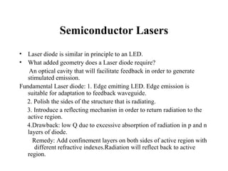
  • 1. Semiconductor Lasers • Laser diode is similar in principle to an LED. • What added geometry does a Laser diode require? An optical cavity that will facilitate feedback in order to generate stimulated emission. Fundamental Laser diode: 1. Edge emitting LED. Edge emission is suitable for adaptation to feedback waveguide. 2. Polish the sides of the structure that is radiating. 3. Introduce a reflecting mechanisn in order to return radiation to the active region. 4.Drawback: low Q due to excessive absorption of radiation in p and n layers of diode. Remedy: Add confinement layers on both sides of active region with different refractive indexes.Radiation will reflect back to active region.
  • 2. Laser Diodes 5. Polishing of the emitting sides of the cavity. A considerable percentage of the radiation is reflected back alone from the difference in reflective indexes of the air- AlGaAs interface. Therefore mirror coating not necessary. Note: radiation propagates from both sides of the device. What function can a photodiode provide in the process? It is attached to the inactive side to serve as a sensor for the power supply in order to provide an element of control of the laser output.
  • 3. Current Cleaved surface mirror L Electrode p+ GaAs L n+ GaAs Electrode Active region (stimulated emission region) A schematic illustration of a GaAs homojunction laser diode. The cleaved surfaces act as reflecting mirrors. © 1999 S.O. Kasap, Optoelectronics (Prentice Hall)
  • 4. Laser Diodes • Lasing occurs when the supply of free electrons exceeds the losses in the cavity. • Current through the junction and the electron supply are directly proportional. I TH must be exceeded before laser action occurs. • Drawback of laser diode: Temperature coefficient.Threshold current increases with temperature. Possible shutdown. Remedy:1. Cooling mechanism. (cooling mount) 2. Constant current power supply with photodetector.
  • 5. Laser Diode Action (intrinsics) Refer to diagram of degenerately doped direct bandgap semiconductor pn junction. Degenerate doping- where fermi level is (EFP ) on P-side is in the valence band (VB)and EFN on the N-side is in the conduction band (CB). ⇒ Energy levels up to the the fermi level are occupied by electrons. ⇒ When there is no applied voltage the fermi level is continuous across the diode ( E FN = E FP ) .
  • 6. p+ Junction n+ Ec Eg p+ n+ eV o Ec EF n In v ers io n reg io n Ec Ev Eg H o les in V B EF n EF p Electro ns i n C B eV Electro ns Ec EF p Ev (a) (b) V The energy band diagram of a degenerately doped p-n with no bias. (b) Band diagram with a sufficiently large forward bias to cause population inversion and hence stimulated emission. © 1999 S.O. Kasap, Optoelectronics (Prentice Hall)
  • 7. Laser Diode (intrinsics) ⇒ Space charge layer (SCL) is very narrow. ⇒ Vo (built in voltage) prevents electrons in CB (n+-side) from diffusing into CB of p+-side. ⇒ There is a similar barrier preventing hole diffusion from p+ to n+ sides. ⇒ Assuming an applied voltage (ev) greater than the bandgap energy,EFN and EFP are now separated by ev. ⇒ eV diminishes barrier potential to 0 allowing electrons to flow into SCL and over to p+-side to establish diode current.
  • 8. Laser Diodes (intrinsics) ⇒ A similar reduction in barrier potential for holes from p+- side to n+-side occurs. ⇒ Result  SCL no longer depleted. E FN − EFP = eV > Eg
  • 9. Laser Diode (Population Inversion) Refer to Density of States. ⇒ More electrons in the CB at energies near Ec than electrons in VB near Ev. ⇒ This is the result of a Population Inversion in energies near EC and EV. ⇒ The region where the population inversion occurs develops a layer along the junction called an inversion layer or active region.
  • 10. Energy Optical gain EF n − EF p CB EF n Electrons Ec in CB eV 0 hυ Eg Ev Holes in VB = Empty states At T > 0 EF p VB At T = 0 Optical absorption Density of states (a) (b) (a) The density of states and energy distribution of electrons and holes in the conduction and valence bands respectively at T ≈ 0 in the SCL under forward bias such that E Fn − E Fp > E g . Holes in the VB are empty states. (b) Gain vs. photon energy. © 1999 S.O. Kasap, Optoelectronics (Prentice Hall)
  • 11. Laser Diode (stimulated emission) An incoming photon with energy of E − E will not see C V electrons to excite from E to E due to the absence of V C electrons at E . V The photon can cause an electron to fall down from E to E . C V The incoming photon is stimulating direct recombination.
  • 12. Laser Diode (stimulated emission) ⇒ The region where there is more stimulated emission than absorption results in Optical gain. ⇒ Optical gain depends upon the photon energy and thus wavelength (see density of states). Summary: *Photons with energy > Eg but < E − E (eV ) cause stimulated FN FP emission. *Photons with energy > E − E (eV ) are absorbed. FN FP
  • 13. Laser Diode (pumping) What is the impact of a temperature increase on Photon energy? The Fermi-Dirac function spreads the energy distributions of electrons in the CB to above E FN and holes below E FP in the VB. Result: a reduction in optical gain. *Optical gain depends on E − E which depends on applied FN FP voltage. In turn this depends on diode current.
  • 14. Laser Diode (pumping) An adequate forward bias is required to develop injection carriers across a junction to initiate a population inversion between energies at E and energies at E . C V What is the pumping mechanism used to achieve this? Forward diode current. The process is called injection pumping.
  • 15. Optical P ower Laser Optical Power Optical P ower LED Stimulated emission λ Optical P ower Laser Spontaneous λ emission I 0 Ith λ Typical output optical power vs. diode current (I) characteristics and the corresponding output spectrum of a laser diode. © 1999 S.O. Kasap, Optoelectronics (Prentice Hall)
  • 16. Laser Diode (optical cavity) In addition to population inversion laser oscillation must be sustained. ⇒ An optical cavity is implemented to elevate the intensity of stimulated emission. (optical resonator) ⇒ Provides an output of continuous coherent radiation. ⇒ A homojunction laser diode is one where the pn junction uses the same direct bandgap semiconductor material throughout the component (ex. GaAs) See slide 3.
  • 17. Laser Diode (optical cavity) The ends of the crystal are cleaved to a flatnessand the ends polished to provide reflection. ⇒ Photons reflected from cleaved surface stimulate more photons of the same frequency. ⇒ The λ of radiation that escalates in the cavity is dependant on the length L of the cavity.(resonant length) ⇒ Only multiples of ½ λ exist. λ m× = L where : m is an integer (mode or resonant frequency) 2n n is the refractive index of the semiconductor λ is the free space wavelength
  • 18. λ m = L where : m is an integer (mode or resonant frequency) 2n n is the refractive index of the semiconductor λ is the free space wavelength λ 2 δλm = 2nL
  • 19. LaserDiode (modes) Separation between the potential modes that can develop, or allowed wavelengths, can be determined by the equation in the previous slide as ∆λm . =>the output spectrum of the laser diode depends upon the nature of the optical cavity and optical gain versus wavelength. Note: lasing radiation occurs when optical gain in the medium can overcome photon losses from the cavity which requires diode current to exceed a threshold current . Light that exists below I th is due to spontaneous emission. Incoherent photons are emitted randomly and devicethbehaves like an I LED.
  • 20. Laser Diodes(output) Lasing oscillations occur when optical gain exceeds photon losses and this is where optical gain reaches threshold gain at I . th • This is the point where modes or resonant frequencies resonate within the cavity. • The polished cavity ends are not perfectly reflecting with approximately 32% transmitting out of cleaved ends. • The number of modes that exist in the output spectrum and their magnitudes depend on the diode current.
  • 21. Laser Diodes (heterostructure) The drawback of a homojunction structure is that the threshold current density ( J th ) is too high and therefore restricted to operating at very low temperatures. Remedy: Heterostructure semiconductor laser diodes. What must be accomplished? - to reduce threshold current to a usable level requires an improvement of the rate of stimulated emission as well as the efficiency of the optical cavity.
  • 22. Laser Diodes (heterostructure) Methods for improvement: 1. Carrier confinement. Confine the injected electrons and holes to a narrow region about the junction. This requires less current to establish the required concentration of electrons for population inversion. 2. Construct a dielectric waveguide around the optical gain region to increase the photon concentration and elevate the probability of stimulated emission. This reduces the number of electrons lost traveling off the cavity axis. Summary: carrier confinement and photon confinement required
  • 23. (a) A double n p p heterostructure diode has two junctions which are (a) AlGaAs GaAs AlGaAs between two different bandgap semiconductors (~0.1 µm) (GaAs and AlGaAs). Electrons in CB Ec ∆Ec (b) Simplified energy Ec 2 eV band diagram under a 2 eV 1.4 eV large forward bias. Lasing recombination (b) Ev takes place in the p- Ev GaAs layer, the active layer Holes in VB Refractive (c) Higher bandgap index materials have a (c) Active ∆n ~ 5% lower refractive region index Photon density (d) AlGaAs layers provide lateral optical (d) confinement. © 1999 S.O. Kasap, Optoelectronics (Prentice Hall)
  • 24. Laser Diodes (double heterostructure) Refer to the slide of the DH structure. =>AlGaAs has Eg of 2 eV ⇒ GaAs has Eg of 1.4 eV ⇒ P-GaAs is a thin layer (0.1 – 0.2 um) and is the Active Layer where lasing recombination occurs. ⇒ Both p regions are heavily doped and are degenereate with in the VB. EF ⇒ With an adequate forward bias Ec of n-AlGaAs moves above Ec of p- GaAs which develops a large injection of electrons from the CB of n- AlGaAs to the CB of p-GaAs. ⇒ These electrons are confined to the CB of the p-GaAs due to the difference in barrier potential of the two materials.
  • 25. Laser Diode (double heterostructure) Note:1.Due to the thin p-GaAs layer a minimal amount of current only is required to increase the concentration of injected carriers at a fast rate. This is how threshold current is reduced for the purpose of poulation inversion and optical gain. 2. A semiconductor with a wider bandgap (AlGaAs) will also have a lower refractive index than GaAs. This difference in refractive index is what establishes an optical dielectric waveguide that ultimately confines photons to the active region.
  • 26. Cleaved reflecting surface W L Stripe electrode Oxide insulator p-GaAs (Contacting layer) p-AlxGa 1-xAs (Confining layer) p-GaAs (Active layer) n-AlxGa 1-xAs (Confining layer) 2 1 3 Current Substrate n-GaAs (Substrate) Substrate paths Electrode Elliptical Cleaved reflecting surface laser Active region where J > Jt h. beam (Emission region) Schematic illustration of the the structure of a double heterojunction stripe contact laser diode © 1999 S.O. Kasap, Optoelectronics (Prentice Hall)
  • 27. Laser Diode (double heterostructure) ⇒ Substrate is n-GaAs ⇒ Confining layers are n-AlGaAs and p-AlGaAs ⇒ Active layer is p-GaAs (870-900nm) ⇒ Additional contacting layer is p-GaAs (allows better electrode contact and avoids Schottky junctions which limit current. ⇒ The p and n-AlGaAs layers provide carrier and optical confinement by forming heterojunctions with the p-GaAs.
  • 28. Laser Diodes(double heterostructure) Advantage of AlGaAs/GaAs heterojunction is that they offer a small lattice mismatch between their crystal structures. This introduces negligible strain induced interfacial defects (dislocations). Defects of this nature act as non-radiative recombination centers.
  • 29. Laser Diode (double heterostructure) Stripe Geometry: =>current density J is not uniform laterally from the stripe contact. =>current is maximum along the central path and diminishes on either side with confinement between path 2 and 3. (gain guided) =>population inversion and therefore optical gain occurs where current density exceeds threshold current values. Adavantages of stripe geometry: 1. Reduced contact reduces threshold current. 2. Reduced emission area makes light coupling to fibre easier. (ex. Stripe widths of a few microns develop threshold currents of tens of milliamperes)
  • 30. Laser Diode (fundamental characteristics) What factors determine LD output spectrum? 1. The neature of the optical resonator that develops laser oscillations. 2. The optical gain curve (line-shape of active medium). =>Optical resonator is a Fabry-Perot cavity. =>length determines longitudinal modes where width and height of the cavity determines transverse or lateral modes. =>with a sufficiently small W and H only the lowest transverse mode exits (TEM ). 00
  • 31. Laser Diode (fundamental characteristics) mode will have longitudinal modes whose separation depends on the length of the cavity. =>Note: the exiting laser beam displays a diverging field due to diffraction at the ends of the cavity. The smaller the aperture the greater the diffraction. =>The spectrum developed is either multimode or single mode determined by the geometry of the optical resonator and the pumping current level. Refer to slide of index guided LD. Note the transition from multimode at low power to single mode at high power. Gain guided LDs tend to stay in multimode.
  • 32. Electrode Oxide insulation p+-AlGaAs (Contacting layer) p-AlGaAs (Confining layer) n-AlGaAs p-GaAs (Active layer) n-AlGaAs (Confining layer) n-GaAs (Substrate) Schematic illustration of the cross sectional structure of a buried heterostructure laser diode. © 1999 S.O. Kasap, Optoelectronics (Prentice Hall)
  • 33. Dielectric mirror Fabry-Perot cavity Length, L Height, H Diffraction Width W limited laser beam The laser cavity definitions and the output laser beam characteristics. © 1999 S.O. Kasap, Optoelectronics (Prentice Hall)
  • 34. Relative optical power P o = 5 mW P o = 3 mW P o = 1 mW λ (nm) 778 780 782 Output spectra of lasing emission from an index guided LD. At sufficiently high diode currents corresponding to high optical power, the operation becomes single mode. (Note: Relative power scale applies to each spectrum individually and not between spectra) © 1999 S.O. Kasap, Optoelectronics (Prentice Hall)
  • 35. Laser Diodes (temperature characteristics) The output characteristics of an LD are sensitive to temperature. =>As temperature increases threshold current increases exponentially. ⇒ Output spectrum also changes. ⇒ A single mode LD will mode hop (jump to a different mode) at certain temperatures. ⇒ This results in a change of laser oscillation wavelength. ⇒ λ increases slowly due to small change in refractive O index and cavity length.
  • 36. P o (mW) 10 0 °C 50 °C 8 25 °C 6 4 2 0 I (mA) 0 20 40 60 80 Output optical power vs. diode current as three different temperatures. The threshold current shifts to higher temperatures. © 1999 S.O. Kasap, Optoelectronics (Prentice Hall)
  • 37. Laser Diodes (temperature characteristics) Remedies if Mode Hop undesirable: 1. Adjust device structure. 2. Implement thermoelectric (TE) cooler. Gain guided LDs inherently have many modes therefore the wavelength vs. temperature behaviour tends to follow the bandgap (optical gain curve as opposed to the cavity properties.
  • 38. Single mode Single mode Multimode 788 (a) (b) (c) 786 784 λo 782 (nm) 780 Mode hopping 778 776 20 30 40 50 20 30 40 50 20 30 40 50 Case temperature (° C) Case temperature (° C) Case temperature (° C) Peak wavelength vs. case temperature characteristics. (a) Mode hops in the output spectrum of a single mode LD. (b) Restricted mode hops and none over the temperature range of interest (20 - 40 °C). (c) Output spectrum from a multimode LD. © 1999 S.O. Kasap, Optoelectronics (Prentice Hall)
  • 39. Laser Diodes (slope efficiency) Slope efficiency determines the optical power ( P ) of the O coherent output radiation related to diode current I th above . P n slope = O I − I th ⇒ W/A or W/mA ⇒ Slope efficiency dependant on device structure and semiconductor package. ⇒ Typically less than 1W/A
  • 40. n Po nth Threshold population n inversion P o = Lasing output power ∝ Nph I Ith Simplified and idealized description of a semiconductor laser diode based on rate equations. Injected electron concentration n and coherent radiation output power Po vs. diode current I. © 1999 S.O. Kasap, Optoelectronics (Prentice Hall)
  • 41. Light power Laser diode 10 mW LED 5 mW Current 0 50 mA 100 mA Typical optical power output vs. forward current for a LED and a laser diode. © 1999 S.O. Kasap, Optoelectronics (Prentice Hall)