SlideShare una empresa de Scribd logo
1 de 25
CNT devices Since their first discovery and fabrication in 1991, CNTs have received considerable attention because of the prospect of new fundamental science  and many potential applications.
Avouris, IBM
Stretching And confined deformation Strain of less than 1% results in the CNT changing from metal to semiconductor.
Twisting and bending
The encapsulated fullerenes can rotate freely in the space of a (10, 10) tube at room temperature, and the rotation of fullerenes will affect C60@ ( 10 ,  10 )  peapod electronic properties significantly; generally, orientational disorderwill remove the sharp features of the average density of states (DOS). However, the rotation of fullerenes cannot induce a metal–insulator transition. Unlike the multicarrier metallic C60@ ( 10 ,  10 )  peapod, the C60@ ( 17 ,  0 )  peapod is a semiconductor, and the effects of the encapsulated fullerenes on tube valence bands and conduction bands are asymmetrical. The distances between the centres of the fullerenes are 0.984 and 1.278 nm for the C60@ ( 10 ,  10 )  peapod and C60@ ( 17 ,  0 )  peapod, respectively. Peapods J. Chen, and J. Dong,  J. Phys. Condens. Matter ,  16,  1401 (2004)
 
It is shown that, by appropriate work function engineering of the source, drain and gate contacts to the device, the following desirable properties should be realizable: a sub-threshold slope close to the thermionic limit; a conductance close to the interfacial limit; an ON/OFF ratio of around 10 00 ; ON current and transconductance close to the low-quantum-capacitance limit. Semiconducting behavior in nanotubes was first reported by Tans  et al.  in 1998. Fig. 5 shows a measurement of the conductance of a semiconducting SWNT as the gate voltage applied to the conducting substrate is varied. The tube conducts at negative Vg and turns off with a positive Vg. The resistance change between the on and off state is many orders of magnitude. This device behavior is analogous to a p-type metal–oxide–semiconductor field-effect transistor (MOSFET), with the nanotube replacing Si as the semiconductor. At large positive gate voltages, n-type conductance is sometimes observed, especially in larger-diameter tubes. McEuen et al.,  IEEE Trans. Nanotechn .,  1 , 78 (2002)
Semiconducting nanotubes are typically p-type at Vg=0 because of the contacts and also because chemical species, particularly oxygen, adsorb on the tube and act as weak p-type dopants. Experiments have shown that changing a tube’s chemical environment can change this doping level—shifting the voltage at which the device turns on by a significant amount. This has spurred interest in nanotubes as chemical sensors. Adsorbate doping can be a problem for reproducible device behavior, however. Controlled chemical doping of tubes, both p- and n-type, has been accomplished in a number of ways. N-type doping was first done using alkali metals that donate electrons to the tube. This has been used to create n-type transistors, p-n junctions, and p-n-p devices. Alkali metals are not air-stable, however, so other techniques are under development, such as using polymers for charge-transfer doping Scattering sites in nanotubes: I–V characteristics at different Vgs for a p-type SWNT FET utilizing an electrolyte gate in order to improve gate efficiency. McEuen et al.,  IEEE Trans. Nanotechn .,  1 , 78 (2002) Implying a mean-free path of approx. 700 nm. Maximum transconductance dI/dVg=20uA/V at Vg=-0.9V. Normalizing this to the device width of ~2nm: 10mS/um.
 
Bottom - gated CNT FET
 
 
Calculated conductance vs gate voltage at room temperature, varying (a) the work function of the metal electrode, and (b) doping of the NT.  In (a) the work function of the metal electrode is changed by - 0 . 2 eV  (red dashed), - 0 . 1 eV  (orange dashed),  0 eV  (green), + 0 . 1 eV  (light blue), and + 0 . 2 eV  (blue), from left to right, respectively. In (b) the doping atomic fraction is  n -type  0.001  (red),  0.0005  (orange), and  0.0001  (green), and  p -type  0.0001  (blue dashed), from left to right, respectively. Thus the gate field induces switching by modulating the contact resistance (the junction barriers). Oxygen adsorption at the junctions modifies the barriers (i.e. the local band-bending of the CNT) and affects the injection of carriers (holes or electrons).
The inverse subthreshold slope, which is a measure of the efficiency of the gate field in turning on the device, decreases with a decrease in gate oxide thickness. This behavior cannot be explained by conventional field-effect transistor models, and has in fact been shown to be a result of the presence of Schottky barriers at the metal/nanotube interface at the source and drain.
There is a clear difference in the inverse subthreshold slope for the case of sweeping all gate segments together ( S = 400 mV/dec) versus sweeping only the inner segments ( S = 180 mV/dec). We attribute the observed change in  S  to a change from Schottky barrier modulation to bulk switching. (b)   shows linear plots of the subthreshold portion  ( where the current is dominated by carrier density )  of the transfer characteristics when the inner gate segments are swept together or separately. The current nearly identical, despite the fact that the effective gate lengths differ by a factor of 1.6 . This is in contrast to the expected behavior of diffusive transport, where the current varies inversely with the gate length.
Calculated output characteristics of the symmetric  ( dashed lines) and the asymmetric  ( solid lines)   CNFET.
 
We have introduced nanotemplate to control selective growth, length and diameter of CNT. Ohmic contact of the CNT/metal interface was formed by rapid thermal annealing (RTA). Diameter control and surface modification of CNT open the possibility to energy band gap modulation.
 
Diode-like rectifying behavior was observed in a CN x  /C multiwalled nanotube due to its being one half doped with nitrogen. FETs   based on an individual CN x  /C nanotube were fabricated by focused ion-beam technology. The nanotube transistors exhibited  n -type semiconductor characteristics, and the conductance of nanotube FETs can be modulated more than four orders of magnitude at room temperature. The electron mobility of a CN x  /C NT FET estimated from its transconductance was as high as 384 0  cm2/Vs. The  n -type gate modulation could be explained as due the effect of bending of the valence band in the Schottky-barrier junction.
CNTs doped with fullerenes inside nanotubes (so-called peapods) are interesting materials for novel CNT FET channels. Transport properties of various peapods such as C60-, Gd@C82-, and Ti2@C92-peapods have been studied by measuring FET  I - V  characteristics. Metallofulleren peapod FETs exhibited ambipolar behavior both p- and n-type characteristics by changing the gate voltage, whereas C60-peapod FETs showed unipolar p-type characteristics similar to the FETs of intact single-walled nanotubes. This difference can be explained in terms of a bandgap narrowing of the single-walled nanotube due to the incorporation of metallofullerenes. The bandgap narrowing was large in the peapods of metallofullerene, where more electrons are transferred from encapsulated metal atoms to the fullerene cages. The entrapped fullerene molecules are capable of modifying the electronic structure of the host tube. It is, therefore,  anticipated that the encapsulation of fullerene molecules can play a role in band gap engineering in nanotubes and hence that peapods may generate conceptually novel molecular devices.
Schematic illustration of elastic strain distributed around the site of metallofullerenes in a small-diameter nanotube peapod and the corresponding changes in conduction and valence band edges. Charge transport in a partially filled peapod FET in “metal-on-top” setup. (a) Transfer characteristics at various temperatures. Data were taken at  V ds  = 0.3 V.
CNT junction Current vs. voltage characteristics of an all-carbon transistor with semiconducting nanotube as channel, with different voltages at the carbon gate. The back gate is kept at 0 V. The measurements were carried out at 4 K.
The band profile of the SB CNTFET at the minimal leakage bias (VG=0V) for VD=0.6V. The band profile of the MOS CNTFET when the source-drain current is low. (VD=0.6V and VG=-0.3V). The channel is a (13,0) nanotube. Ambipolar conduction leads to a large leakage current that exponentially increases with the power supply voltage, especially when the tube diameter is large. An asymmetric gate oxide SB CNTFET has been proposed as a means of suppressing ambipolar conduction. SB CNTFETs of any type, however, will likely suffer from the need to place the gate electrode close to the source (which increases parasitic capacitance) and metal-induced gap states, which increase source to drain tunneling and limit the minimum channel length.
Id vs. Vd characteristics at VG = 0.4V for the MOS CNTFET (the solid line) and the SB CNTFETs (the dashed lines). The off-current of all transistors (defined at Vd=0.4V and Vg=0) was set at  0.01 µA  by adjusting the flat band voltage for each transistor. For the SB CNTFETs, three barrier heights we simulated. The channel is a (13,0) nanotube, which results in a diameter of  d≈ 1 nm , and a bandgap of  Eg≈ 0.83 eV . Id vs. Vg characteristics at  Vd   = 0.4V  for the zero barrier SBFET and the MOS CNTFET. The gated channel of both transistors is a 5nm-long, intrinsic (13, 0) CNT. By eliminating the Schottky barrier between the source and channel, the transistor will be capable of delivering more on-current. The leakage current of such devices will be controlled by the full bandgap of CNTs (instead of half of the bandgap for SB CNTFETs) and band-to-band tunneling. These factors will depend on the diameter of nanotubes and the power supply voltage.

Más contenido relacionado

La actualidad más candente

Poster_STEM_Research
Poster_STEM_ResearchPoster_STEM_Research
Poster_STEM_Research
Jada Gray
 
33nd battery conference poster zhou TB JC
33nd battery conference poster zhou TB JC33nd battery conference poster zhou TB JC
33nd battery conference poster zhou TB JC
Jigang Zhou
 
Carbon nanotube
Carbon nanotubeCarbon nanotube
Carbon nanotube
mayur141
 
Graphene and hexagonal boron nitride filled epoxy nanocomposites
Graphene and hexagonal boron nitride filled epoxy nanocompositesGraphene and hexagonal boron nitride filled epoxy nanocomposites
Graphene and hexagonal boron nitride filled epoxy nanocomposites
Arun Yadav
 

La actualidad más candente (19)

CNFET Technology
CNFET TechnologyCNFET Technology
CNFET Technology
 
Performance analysis of cntfet and mosfet focusing channel length, carrier mo...
Performance analysis of cntfet and mosfet focusing channel length, carrier mo...Performance analysis of cntfet and mosfet focusing channel length, carrier mo...
Performance analysis of cntfet and mosfet focusing channel length, carrier mo...
 
CNTFET
CNTFETCNTFET
CNTFET
 
Reconfigurable Double Gate CNTFET Based Nanoelectronic Architecture
Reconfigurable Double Gate CNTFET Based Nanoelectronic Architecture Reconfigurable Double Gate CNTFET Based Nanoelectronic Architecture
Reconfigurable Double Gate CNTFET Based Nanoelectronic Architecture
 
CNTFET Based Analog and Digital Circuit Designing: A Review
CNTFET Based Analog and Digital Circuit Designing: A ReviewCNTFET Based Analog and Digital Circuit Designing: A Review
CNTFET Based Analog and Digital Circuit Designing: A Review
 
Carbon Nanotubes
Carbon NanotubesCarbon Nanotubes
Carbon Nanotubes
 
Cntfet technology
Cntfet technologyCntfet technology
Cntfet technology
 
Carbon nanotube
Carbon nanotubeCarbon nanotube
Carbon nanotube
 
Synthesis of CNT by Arc discharge method
Synthesis of CNT by Arc discharge methodSynthesis of CNT by Arc discharge method
Synthesis of CNT by Arc discharge method
 
Poster_STEM_Research
Poster_STEM_ResearchPoster_STEM_Research
Poster_STEM_Research
 
METHODS FOR SYNTHESIS OF CNT
METHODS FOR SYNTHESIS OF CNTMETHODS FOR SYNTHESIS OF CNT
METHODS FOR SYNTHESIS OF CNT
 
Pentacene-Based Organic Field-Effect Transistors: Analytical Model and Simula...
Pentacene-Based Organic Field-Effect Transistors: Analytical Model and Simula...Pentacene-Based Organic Field-Effect Transistors: Analytical Model and Simula...
Pentacene-Based Organic Field-Effect Transistors: Analytical Model and Simula...
 
GNR FET
GNR FET GNR FET
GNR FET
 
Carbon nanotube tissues for high flexible li ion batteries (vinsensia ade sug...
Carbon nanotube tissues for high flexible li ion batteries (vinsensia ade sug...Carbon nanotube tissues for high flexible li ion batteries (vinsensia ade sug...
Carbon nanotube tissues for high flexible li ion batteries (vinsensia ade sug...
 
33nd battery conference poster zhou TB JC
33nd battery conference poster zhou TB JC33nd battery conference poster zhou TB JC
33nd battery conference poster zhou TB JC
 
Carbon nanotube
Carbon nanotubeCarbon nanotube
Carbon nanotube
 
GAA nano wire FET
GAA nano wire FETGAA nano wire FET
GAA nano wire FET
 
Graphene and hexagonal boron nitride filled epoxy nanocomposites
Graphene and hexagonal boron nitride filled epoxy nanocompositesGraphene and hexagonal boron nitride filled epoxy nanocomposites
Graphene and hexagonal boron nitride filled epoxy nanocomposites
 
Conducting polymers based nanocomposites for flexible supercapacitors
Conducting polymers based nanocomposites for flexible supercapacitorsConducting polymers based nanocomposites for flexible supercapacitors
Conducting polymers based nanocomposites for flexible supercapacitors
 

Destacado

Güneş panelleri .1
Güneş panelleri .1Güneş panelleri .1
Güneş panelleri .1
Habip TAYLAN
 
Güneş panelleri ve nano teknoloji kullanımı
Güneş panelleri ve nano teknoloji kullanımıGüneş panelleri ve nano teknoloji kullanımı
Güneş panelleri ve nano teknoloji kullanımı
Habip TAYLAN
 
Nanotechnology Power Point 1
Nanotechnology Power Point 1Nanotechnology Power Point 1
Nanotechnology Power Point 1
lusik
 
Applications of carbon nanotubes
Applications of carbon nanotubesApplications of carbon nanotubes
Applications of carbon nanotubes
Nitin Patel
 
Supercapacitor
SupercapacitorSupercapacitor
Supercapacitor
Saleem Mir
 

Destacado (20)

Carbon nanotubes (cnt) as interconnects for future
Carbon nanotubes (cnt) as interconnects for futureCarbon nanotubes (cnt) as interconnects for future
Carbon nanotubes (cnt) as interconnects for future
 
Güneş panelleri .1
Güneş panelleri .1Güneş panelleri .1
Güneş panelleri .1
 
Güneş panelleri ve nano teknoloji kullanımı
Güneş panelleri ve nano teknoloji kullanımıGüneş panelleri ve nano teknoloji kullanımı
Güneş panelleri ve nano teknoloji kullanımı
 
ARIANA SANCHEZ EMPRESA CNT
ARIANA SANCHEZ EMPRESA CNTARIANA SANCHEZ EMPRESA CNT
ARIANA SANCHEZ EMPRESA CNT
 
Ajit K.
Ajit K.Ajit K.
Ajit K.
 
Nano-bio Dr Nedra Karunaratne
Nano-bio Dr Nedra Karunaratne Nano-bio Dr Nedra Karunaratne
Nano-bio Dr Nedra Karunaratne
 
Wedn. cnt ppt
Wedn. cnt pptWedn. cnt ppt
Wedn. cnt ppt
 
Carbon nanotubes for adsorption of organic contaminants
Carbon nanotubes for adsorption of organic contaminantsCarbon nanotubes for adsorption of organic contaminants
Carbon nanotubes for adsorption of organic contaminants
 
Nanotechnology Power Point 1
Nanotechnology Power Point 1Nanotechnology Power Point 1
Nanotechnology Power Point 1
 
nano bio
nano bionano bio
nano bio
 
cnt ppt
cnt pptcnt ppt
cnt ppt
 
Nano-electronics
Nano-electronicsNano-electronics
Nano-electronics
 
Graphite,Fullerene And Carbon Nanotubules
Graphite,Fullerene And Carbon NanotubulesGraphite,Fullerene And Carbon Nanotubules
Graphite,Fullerene And Carbon Nanotubules
 
Epoxy/CNT nanocomposites
Epoxy/CNT nanocompositesEpoxy/CNT nanocomposites
Epoxy/CNT nanocomposites
 
Tez sunum
Tez sunumTez sunum
Tez sunum
 
Supercapacitors
SupercapacitorsSupercapacitors
Supercapacitors
 
Supercapacitors ppt hhd
Supercapacitors ppt hhdSupercapacitors ppt hhd
Supercapacitors ppt hhd
 
Carbon and Low-Alloy Steels for Non-Metallurgists
Carbon and Low-Alloy Steels for Non-MetallurgistsCarbon and Low-Alloy Steels for Non-Metallurgists
Carbon and Low-Alloy Steels for Non-Metallurgists
 
Applications of carbon nanotubes
Applications of carbon nanotubesApplications of carbon nanotubes
Applications of carbon nanotubes
 
Supercapacitor
SupercapacitorSupercapacitor
Supercapacitor
 

Similar a Cnt devices

CNT as Field Effect Transistor application
CNT as Field Effect Transistor applicationCNT as Field Effect Transistor application
CNT as Field Effect Transistor application
yihovo9909
 
E L S E V I E R Microelectronic Engineering 46 (1999) 101-104.docx
E L S E V I E R  Microelectronic Engineering 46 (1999) 101-104.docxE L S E V I E R  Microelectronic Engineering 46 (1999) 101-104.docx
E L S E V I E R Microelectronic Engineering 46 (1999) 101-104.docx
sagarlesley
 
Carbon nanotube field-effect transistor - Wikipedia.pdf
Carbon nanotube field-effect transistor - Wikipedia.pdfCarbon nanotube field-effect transistor - Wikipedia.pdf
Carbon nanotube field-effect transistor - Wikipedia.pdf
SANTHOSH57966
 
Introduction gadgets have gained a lot of attention.pdf
Introduction gadgets have gained a lot of attention.pdfIntroduction gadgets have gained a lot of attention.pdf
Introduction gadgets have gained a lot of attention.pdf
bkbk37
 
Nanoelectronics Final
Nanoelectronics FinalNanoelectronics Final
Nanoelectronics Final
shikha2510
 
Welcome to International Journal of Engineering Research and Development (IJERD)
Welcome to International Journal of Engineering Research and Development (IJERD)Welcome to International Journal of Engineering Research and Development (IJERD)
Welcome to International Journal of Engineering Research and Development (IJERD)
IJERD Editor
 
CNT(Microelectron. Reliab)
CNT(Microelectron. Reliab)CNT(Microelectron. Reliab)
CNT(Microelectron. Reliab)
Wei-Chih Chiu
 

Similar a Cnt devices (20)

CNT as Field Effect Transistor application
CNT as Field Effect Transistor applicationCNT as Field Effect Transistor application
CNT as Field Effect Transistor application
 
E L S E V I E R Microelectronic Engineering 46 (1999) 101-104.docx
E L S E V I E R  Microelectronic Engineering 46 (1999) 101-104.docxE L S E V I E R  Microelectronic Engineering 46 (1999) 101-104.docx
E L S E V I E R Microelectronic Engineering 46 (1999) 101-104.docx
 
Carbon nanotube field-effect transistor - Wikipedia.pdf
Carbon nanotube field-effect transistor - Wikipedia.pdfCarbon nanotube field-effect transistor - Wikipedia.pdf
Carbon nanotube field-effect transistor - Wikipedia.pdf
 
Nano
NanoNano
Nano
 
Introduction gadgets have gained a lot of attention.pdf
Introduction gadgets have gained a lot of attention.pdfIntroduction gadgets have gained a lot of attention.pdf
Introduction gadgets have gained a lot of attention.pdf
 
Cntfet
Cntfet   Cntfet
Cntfet
 
Master's Thesis Presentation
Master's Thesis PresentationMaster's Thesis Presentation
Master's Thesis Presentation
 
ECE 6030 Device Electronics.docx
ECE 6030 Device Electronics.docxECE 6030 Device Electronics.docx
ECE 6030 Device Electronics.docx
 
Properties Of Cnt
Properties Of CntProperties Of Cnt
Properties Of Cnt
 
Nanoelectronics Final
Nanoelectronics FinalNanoelectronics Final
Nanoelectronics Final
 
Welcome to International Journal of Engineering Research and Development (IJERD)
Welcome to International Journal of Engineering Research and Development (IJERD)Welcome to International Journal of Engineering Research and Development (IJERD)
Welcome to International Journal of Engineering Research and Development (IJERD)
 
Analytical Modeling of Tunneling Field Effect Transistor (TFET)
Analytical Modeling of Tunneling Field Effect Transistor (TFET)Analytical Modeling of Tunneling Field Effect Transistor (TFET)
Analytical Modeling of Tunneling Field Effect Transistor (TFET)
 
Cnt flow-sensorss
Cnt flow-sensorssCnt flow-sensorss
Cnt flow-sensorss
 
CNT Ballistic Transistor
CNT Ballistic TransistorCNT Ballistic Transistor
CNT Ballistic Transistor
 
Carbon Nano tubes and its Applications in the Field of Electronics and Comput...
Carbon Nano tubes and its Applications in the Field of Electronics and Comput...Carbon Nano tubes and its Applications in the Field of Electronics and Comput...
Carbon Nano tubes and its Applications in the Field of Electronics and Comput...
 
Carbonnanotubes
Carbonnanotubes Carbonnanotubes
Carbonnanotubes
 
Carbonnanotubes
CarbonnanotubesCarbonnanotubes
Carbonnanotubes
 
CARBON NANO TUBES
CARBON NANO TUBESCARBON NANO TUBES
CARBON NANO TUBES
 
CNT(Microelectron. Reliab)
CNT(Microelectron. Reliab)CNT(Microelectron. Reliab)
CNT(Microelectron. Reliab)
 
A Comparative Performance Analysis of Copper on Chip and CNTFET Nano Intercon...
A Comparative Performance Analysis of Copper on Chip and CNTFET Nano Intercon...A Comparative Performance Analysis of Copper on Chip and CNTFET Nano Intercon...
A Comparative Performance Analysis of Copper on Chip and CNTFET Nano Intercon...
 

Último

Making and Justifying Mathematical Decisions.pdf
Making and Justifying Mathematical Decisions.pdfMaking and Justifying Mathematical Decisions.pdf
Making and Justifying Mathematical Decisions.pdf
Chris Hunter
 

Último (20)

PROCESS RECORDING FORMAT.docx
PROCESS      RECORDING        FORMAT.docxPROCESS      RECORDING        FORMAT.docx
PROCESS RECORDING FORMAT.docx
 
Mixin Classes in Odoo 17 How to Extend Models Using Mixin Classes
Mixin Classes in Odoo 17  How to Extend Models Using Mixin ClassesMixin Classes in Odoo 17  How to Extend Models Using Mixin Classes
Mixin Classes in Odoo 17 How to Extend Models Using Mixin Classes
 
Introduction to Nonprofit Accounting: The Basics
Introduction to Nonprofit Accounting: The BasicsIntroduction to Nonprofit Accounting: The Basics
Introduction to Nonprofit Accounting: The Basics
 
APM Welcome, APM North West Network Conference, Synergies Across Sectors
APM Welcome, APM North West Network Conference, Synergies Across SectorsAPM Welcome, APM North West Network Conference, Synergies Across Sectors
APM Welcome, APM North West Network Conference, Synergies Across Sectors
 
microwave assisted reaction. General introduction
microwave assisted reaction. General introductionmicrowave assisted reaction. General introduction
microwave assisted reaction. General introduction
 
Advance Mobile Application Development class 07
Advance Mobile Application Development class 07Advance Mobile Application Development class 07
Advance Mobile Application Development class 07
 
Basic Civil Engineering first year Notes- Chapter 4 Building.pptx
Basic Civil Engineering first year Notes- Chapter 4 Building.pptxBasic Civil Engineering first year Notes- Chapter 4 Building.pptx
Basic Civil Engineering first year Notes- Chapter 4 Building.pptx
 
Making and Justifying Mathematical Decisions.pdf
Making and Justifying Mathematical Decisions.pdfMaking and Justifying Mathematical Decisions.pdf
Making and Justifying Mathematical Decisions.pdf
 
This PowerPoint helps students to consider the concept of infinity.
This PowerPoint helps students to consider the concept of infinity.This PowerPoint helps students to consider the concept of infinity.
This PowerPoint helps students to consider the concept of infinity.
 
Unit-IV; Professional Sales Representative (PSR).pptx
Unit-IV; Professional Sales Representative (PSR).pptxUnit-IV; Professional Sales Representative (PSR).pptx
Unit-IV; Professional Sales Representative (PSR).pptx
 
Grant Readiness 101 TechSoup and Remy Consulting
Grant Readiness 101 TechSoup and Remy ConsultingGrant Readiness 101 TechSoup and Remy Consulting
Grant Readiness 101 TechSoup and Remy Consulting
 
Sports & Fitness Value Added Course FY..
Sports & Fitness Value Added Course FY..Sports & Fitness Value Added Course FY..
Sports & Fitness Value Added Course FY..
 
Z Score,T Score, Percential Rank and Box Plot Graph
Z Score,T Score, Percential Rank and Box Plot GraphZ Score,T Score, Percential Rank and Box Plot Graph
Z Score,T Score, Percential Rank and Box Plot Graph
 
SECOND SEMESTER TOPIC COVERAGE SY 2023-2024 Trends, Networks, and Critical Th...
SECOND SEMESTER TOPIC COVERAGE SY 2023-2024 Trends, Networks, and Critical Th...SECOND SEMESTER TOPIC COVERAGE SY 2023-2024 Trends, Networks, and Critical Th...
SECOND SEMESTER TOPIC COVERAGE SY 2023-2024 Trends, Networks, and Critical Th...
 
Presentation by Andreas Schleicher Tackling the School Absenteeism Crisis 30 ...
Presentation by Andreas Schleicher Tackling the School Absenteeism Crisis 30 ...Presentation by Andreas Schleicher Tackling the School Absenteeism Crisis 30 ...
Presentation by Andreas Schleicher Tackling the School Absenteeism Crisis 30 ...
 
Nutritional Needs Presentation - HLTH 104
Nutritional Needs Presentation - HLTH 104Nutritional Needs Presentation - HLTH 104
Nutritional Needs Presentation - HLTH 104
 
Paris 2024 Olympic Geographies - an activity
Paris 2024 Olympic Geographies - an activityParis 2024 Olympic Geographies - an activity
Paris 2024 Olympic Geographies - an activity
 
Advanced Views - Calendar View in Odoo 17
Advanced Views - Calendar View in Odoo 17Advanced Views - Calendar View in Odoo 17
Advanced Views - Calendar View in Odoo 17
 
Key note speaker Neum_Admir Softic_ENG.pdf
Key note speaker Neum_Admir Softic_ENG.pdfKey note speaker Neum_Admir Softic_ENG.pdf
Key note speaker Neum_Admir Softic_ENG.pdf
 
Holdier Curriculum Vitae (April 2024).pdf
Holdier Curriculum Vitae (April 2024).pdfHoldier Curriculum Vitae (April 2024).pdf
Holdier Curriculum Vitae (April 2024).pdf
 

Cnt devices

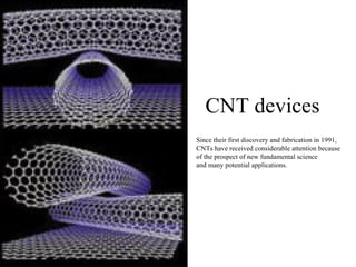
  • 1. CNT devices Since their first discovery and fabrication in 1991, CNTs have received considerable attention because of the prospect of new fundamental science and many potential applications.
  • 3. Stretching And confined deformation Strain of less than 1% results in the CNT changing from metal to semiconductor.
  • 5. The encapsulated fullerenes can rotate freely in the space of a (10, 10) tube at room temperature, and the rotation of fullerenes will affect C60@ ( 10 , 10 ) peapod electronic properties significantly; generally, orientational disorderwill remove the sharp features of the average density of states (DOS). However, the rotation of fullerenes cannot induce a metal–insulator transition. Unlike the multicarrier metallic C60@ ( 10 , 10 ) peapod, the C60@ ( 17 , 0 ) peapod is a semiconductor, and the effects of the encapsulated fullerenes on tube valence bands and conduction bands are asymmetrical. The distances between the centres of the fullerenes are 0.984 and 1.278 nm for the C60@ ( 10 , 10 ) peapod and C60@ ( 17 , 0 ) peapod, respectively. Peapods J. Chen, and J. Dong, J. Phys. Condens. Matter , 16, 1401 (2004)
  • 6.  
  • 7. It is shown that, by appropriate work function engineering of the source, drain and gate contacts to the device, the following desirable properties should be realizable: a sub-threshold slope close to the thermionic limit; a conductance close to the interfacial limit; an ON/OFF ratio of around 10 00 ; ON current and transconductance close to the low-quantum-capacitance limit. Semiconducting behavior in nanotubes was first reported by Tans et al. in 1998. Fig. 5 shows a measurement of the conductance of a semiconducting SWNT as the gate voltage applied to the conducting substrate is varied. The tube conducts at negative Vg and turns off with a positive Vg. The resistance change between the on and off state is many orders of magnitude. This device behavior is analogous to a p-type metal–oxide–semiconductor field-effect transistor (MOSFET), with the nanotube replacing Si as the semiconductor. At large positive gate voltages, n-type conductance is sometimes observed, especially in larger-diameter tubes. McEuen et al., IEEE Trans. Nanotechn ., 1 , 78 (2002)
  • 8. Semiconducting nanotubes are typically p-type at Vg=0 because of the contacts and also because chemical species, particularly oxygen, adsorb on the tube and act as weak p-type dopants. Experiments have shown that changing a tube’s chemical environment can change this doping level—shifting the voltage at which the device turns on by a significant amount. This has spurred interest in nanotubes as chemical sensors. Adsorbate doping can be a problem for reproducible device behavior, however. Controlled chemical doping of tubes, both p- and n-type, has been accomplished in a number of ways. N-type doping was first done using alkali metals that donate electrons to the tube. This has been used to create n-type transistors, p-n junctions, and p-n-p devices. Alkali metals are not air-stable, however, so other techniques are under development, such as using polymers for charge-transfer doping Scattering sites in nanotubes: I–V characteristics at different Vgs for a p-type SWNT FET utilizing an electrolyte gate in order to improve gate efficiency. McEuen et al., IEEE Trans. Nanotechn ., 1 , 78 (2002) Implying a mean-free path of approx. 700 nm. Maximum transconductance dI/dVg=20uA/V at Vg=-0.9V. Normalizing this to the device width of ~2nm: 10mS/um.
  • 9.  
  • 10. Bottom - gated CNT FET
  • 11.  
  • 12.  
  • 13. Calculated conductance vs gate voltage at room temperature, varying (a) the work function of the metal electrode, and (b) doping of the NT. In (a) the work function of the metal electrode is changed by - 0 . 2 eV (red dashed), - 0 . 1 eV (orange dashed), 0 eV (green), + 0 . 1 eV (light blue), and + 0 . 2 eV (blue), from left to right, respectively. In (b) the doping atomic fraction is n -type 0.001 (red), 0.0005 (orange), and 0.0001 (green), and p -type 0.0001 (blue dashed), from left to right, respectively. Thus the gate field induces switching by modulating the contact resistance (the junction barriers). Oxygen adsorption at the junctions modifies the barriers (i.e. the local band-bending of the CNT) and affects the injection of carriers (holes or electrons).
  • 14. The inverse subthreshold slope, which is a measure of the efficiency of the gate field in turning on the device, decreases with a decrease in gate oxide thickness. This behavior cannot be explained by conventional field-effect transistor models, and has in fact been shown to be a result of the presence of Schottky barriers at the metal/nanotube interface at the source and drain.
  • 15. There is a clear difference in the inverse subthreshold slope for the case of sweeping all gate segments together ( S = 400 mV/dec) versus sweeping only the inner segments ( S = 180 mV/dec). We attribute the observed change in S to a change from Schottky barrier modulation to bulk switching. (b) shows linear plots of the subthreshold portion ( where the current is dominated by carrier density ) of the transfer characteristics when the inner gate segments are swept together or separately. The current nearly identical, despite the fact that the effective gate lengths differ by a factor of 1.6 . This is in contrast to the expected behavior of diffusive transport, where the current varies inversely with the gate length.
  • 16. Calculated output characteristics of the symmetric ( dashed lines) and the asymmetric ( solid lines) CNFET.
  • 17.  
  • 18. We have introduced nanotemplate to control selective growth, length and diameter of CNT. Ohmic contact of the CNT/metal interface was formed by rapid thermal annealing (RTA). Diameter control and surface modification of CNT open the possibility to energy band gap modulation.
  • 19.  
  • 20. Diode-like rectifying behavior was observed in a CN x /C multiwalled nanotube due to its being one half doped with nitrogen. FETs based on an individual CN x /C nanotube were fabricated by focused ion-beam technology. The nanotube transistors exhibited n -type semiconductor characteristics, and the conductance of nanotube FETs can be modulated more than four orders of magnitude at room temperature. The electron mobility of a CN x /C NT FET estimated from its transconductance was as high as 384 0 cm2/Vs. The n -type gate modulation could be explained as due the effect of bending of the valence band in the Schottky-barrier junction.
  • 21. CNTs doped with fullerenes inside nanotubes (so-called peapods) are interesting materials for novel CNT FET channels. Transport properties of various peapods such as C60-, Gd@C82-, and Ti2@C92-peapods have been studied by measuring FET I - V characteristics. Metallofulleren peapod FETs exhibited ambipolar behavior both p- and n-type characteristics by changing the gate voltage, whereas C60-peapod FETs showed unipolar p-type characteristics similar to the FETs of intact single-walled nanotubes. This difference can be explained in terms of a bandgap narrowing of the single-walled nanotube due to the incorporation of metallofullerenes. The bandgap narrowing was large in the peapods of metallofullerene, where more electrons are transferred from encapsulated metal atoms to the fullerene cages. The entrapped fullerene molecules are capable of modifying the electronic structure of the host tube. It is, therefore, anticipated that the encapsulation of fullerene molecules can play a role in band gap engineering in nanotubes and hence that peapods may generate conceptually novel molecular devices.
  • 22. Schematic illustration of elastic strain distributed around the site of metallofullerenes in a small-diameter nanotube peapod and the corresponding changes in conduction and valence band edges. Charge transport in a partially filled peapod FET in “metal-on-top” setup. (a) Transfer characteristics at various temperatures. Data were taken at V ds = 0.3 V.
  • 23. CNT junction Current vs. voltage characteristics of an all-carbon transistor with semiconducting nanotube as channel, with different voltages at the carbon gate. The back gate is kept at 0 V. The measurements were carried out at 4 K.
  • 24. The band profile of the SB CNTFET at the minimal leakage bias (VG=0V) for VD=0.6V. The band profile of the MOS CNTFET when the source-drain current is low. (VD=0.6V and VG=-0.3V). The channel is a (13,0) nanotube. Ambipolar conduction leads to a large leakage current that exponentially increases with the power supply voltage, especially when the tube diameter is large. An asymmetric gate oxide SB CNTFET has been proposed as a means of suppressing ambipolar conduction. SB CNTFETs of any type, however, will likely suffer from the need to place the gate electrode close to the source (which increases parasitic capacitance) and metal-induced gap states, which increase source to drain tunneling and limit the minimum channel length.
  • 25. Id vs. Vd characteristics at VG = 0.4V for the MOS CNTFET (the solid line) and the SB CNTFETs (the dashed lines). The off-current of all transistors (defined at Vd=0.4V and Vg=0) was set at 0.01 µA by adjusting the flat band voltage for each transistor. For the SB CNTFETs, three barrier heights we simulated. The channel is a (13,0) nanotube, which results in a diameter of d≈ 1 nm , and a bandgap of Eg≈ 0.83 eV . Id vs. Vg characteristics at Vd = 0.4V for the zero barrier SBFET and the MOS CNTFET. The gated channel of both transistors is a 5nm-long, intrinsic (13, 0) CNT. By eliminating the Schottky barrier between the source and channel, the transistor will be capable of delivering more on-current. The leakage current of such devices will be controlled by the full bandgap of CNTs (instead of half of the bandgap for SB CNTFETs) and band-to-band tunneling. These factors will depend on the diameter of nanotubes and the power supply voltage.