SlideShare una empresa de Scribd logo
1 de 30
The Logic "AND" Gate
Definition
A Logic AND Gate is a type of digital logic gate that has an output which is normally at logic
level "0" and only goes "HIGH" to a logic level "1" when ALL of its inputs are at logic level
"1". The output of a Logic AND Gate only returns "LOW" again when ANY of its inputs are at
a logic level "0". The logic or Boolean expression given for a logic AND gate is that for Logical
Multiplication which is denoted by a single dot or full stop symbol, ( . ) giving us the Boolean
expression of: A.B = Q.

Then we can define the operation of a 2-input logic AND gate as being:

                            "If both A and B are true, then Q is true"

The Digital Logic "AND" Gate
2-input AND Gate
                         Symbol                                     Truth Table
                                                           B             A           Q
                                                           0             0            0
                                                           0             1            0
                   2-input AND Gate                        1             0            0
                                                           1             1            1
              Boolean Expression Q = A.B                    Read as A AND B gives Q


3-input AND Gate
                      Symbol                                     Truth Table
                                                    C           B            A        Q
                                                     0          0            0         0
                                                     0          0            1         0
                                                     0          1            0         0
                3-input AND Gate                     0          1            1         0
                                                     1          0            0         0
1          0          1           0
                                                    1          1          0           0
                                                    1          1          1           1
          Boolean Expression Q = A.B.C              Read as A AND B AND C gives Q


Because the Boolean expression for the logic AND function is defined as (.), which is a binary
operation, AND gates can be cascaded together to form any number of individual inputs.
However, commercial available AND gate IC's are only available in standard 2, 3, or 4-input
packages. If additional inputs are required, then standard AND gates will need to be cascaded
together to obtain the required input value, for example.

Multi-input AND Gate


The Boolean Expression for this 6-input AND gate will therefore be: Q = (A.B).(C.D).(E.F)

The Logic "OR" Gate
Definition
A Logic OR Gate or Inclusive-OR gate is a type of digital logic gate that has an output which is
normally at logic level "0" and only goes "HIGH" to a logic level "1" when one or more of its
inputs are at logic level "1". The output, Q of a Logic OR Gate only returns "LOW" again when
ALL of its inputs are at a logic level "0". The logic or Boolean expression given for a logic OR
gate is that for Logical Addition which is denoted by a plus sign, ( + ) giving us the Boolean
expression of: A+B = Q.

Then we can define the operation of a 2-input logic OR gate as being:
"If either A or B is true, then Q is true"


The Digital Logic "OR" Gate
2-input OR Gate
                         Symbol                                        Truth Table
                                                             B             A          Q
                                                              0            0           0
                                                              0            1           1
                     2-input OR Gate                          1            0           1
                                                              1            1           1
              Boolean Expression Q = A+B                       Read as A OR B gives Q


3-input OR Gate
                       Symbol                                      Truth Table
                                                       C           B           A        Q
                                                       0           0           0        0
                                                       0           0           1        1
                                                       0           1           0        1
                                                       0           1           1        1
                  3-input OR Gate                      1           0           0        1
                                                       1           0           1        1
                                                       1           1           0        1
                                                       1           1           1        1
          Boolean Expression Q = A+B+C                   Read as A OR B OR C gives Q

Like the AND gate, the OR function can have any number of individual inputs. However,
commercial available OR gates are available in 2, 3, or 4 inputs types. Additional inputs will
require gates to be cascaded together for example.

Multi-input OR Gate
The Boolean Expression for this 6-input OR gate will therefore be: Q = (A+B)+(C+D)+(E+F)

The Digital Logic "NOT" Gate
Definition
The digital Logic NOT Gate is the most basic of all the logical gates and is sometimes referred
to as an Inverting Buffer or simply a Digital Inverter. It is a single input device which has an
output level that is normally at logic level "1" and goes "LOW" to a logic level "0" when its
single input is at logic level "1", in other words it "inverts" (complements) its input signal. The
output from a NOT gate only returns "HIGH" again when its input is at logic level "0" giving us
the Boolean expression of: A = Q.

Then we can define the operation of a single input logic NOT gate as being:

                                "If A is NOT true, then Q is true"


The Digital Inverter or NOT gate
                         Symbol                                      Truth Table
                                                                A                   Q
                                                                0                   1

                  Inverter or NOT Gate                          1                   0
          Boolean Expression Q = not A or A                 Read as inverse of A gives Q
Logic NOT gates provide the complement of their input signal and are so called because when
their input signal is "HIGH" their output state will NOT be "HIGH". Likewise, when their input
signal is "LOW" their output state will NOT be "LOW". As they are single input devices, logic
NOT gates are not normally classed as "decision" making devices or even as a gate, such as the
AND or OR gates which have two or more logic inputs. Commercial available NOT gates IC's
are available in either 4 or 6 individual gates within a single i.c. package.

The Logic "NAND" Gate
Definition
The Logic NAND Gate is a combination of the digital logic AND gate with that of an inverter or
NOT gate connected together in series. The NAND (Not - AND) gate has an output that is
normally at logic level "1" and only goes "LOW" to logic level "0" when ALL of its inputs are at
logic level "1". The Logic NAND Gate is the reverse or "Complementary" form of the AND
gate we have seen previously.

Logic NAND Gate Equivalence


The logic or Boolean expression given for a logic NAND gate is that for Logical Addition, which
is the opposite to the AND gate, and which it performs on the complements of the inputs. The
Boolean expression for a logic NAND gate is denoted by a single dot or full stop symbol, ( . )
with a line or Overline, ( ‾‾ ) over the expression to signify the NOT or logical negation of the
NAND gate giving us the Boolean expression of: A.B = Q.

The Digital Logic "NAND" Gate
2-input NAND Gate
                      Symbol                                    Truth Table
                                                      B              A              Q
                                                       0             0              1
                                                       0             1              1
                2-input NAND Gate                      1             0              1
                                                       1             1              0
Boolean Expression Q = A.B                 Read as A AND B gives NOT Q


3-input NAND Gate
                    Symbol                                    Truth Table
                                                 C           B           A           Q
                                                 0           0           0           1
                                                 0           0           1           1
                                                 0           1           0           1
                                                 0           1           1           1
              3-input NAND Gate                  1           0           0           1
                                                 1           0           1           1
                                                 1           1           0           1
                                                 1           1           1           0
        Boolean Expression Q = A.B.C           Read as A AND B AND C gives NOT Q


As with the AND function seen previously, the NAND function can also have any number of
individual inputs and commercial available NAND Gate i.c.´s are available in standard 2, 3, or 4
input types

The Logic "NOR" Gate
Definition
The Logic NOR Gate or Inclusive-NOR gate is a combination of the digital logic OR gate with
that of an inverter or NOT gate connected together in series. The NOR (Not - OR) gate has an
output that is normally at logic level "1" and only goes "LOW" to logic level "0" when ANY of
its inputs are at logic level "1". The Logic NOR Gate is the reverse or "Complementary" form of
the OR gate we have seen previously.

NOR Gate Equivalent


The logic or Boolean expression given for a logic NOR gate is that for Logical Multiplication
which it performs on the complements of the inputs. The Boolean expression for a logic NOR
gate is denoted by a plus sign, ( + ) with a line or Overline, ( ‾‾ ) over the expression to signify
the NOT or logical negation of the NOR gate giving us the Boolean expression of: A+B = Q.

Then we can define the operation of a 2-input logic NOR gate as being:

                           "If both A and B are NOT true, then Q is true"


The Digital Logic "NOR" Gate
2-input NOR Gate
                        Symbol                                        Truth Table
                                                           B              A              Q
                                                           0              0               1
                                                           0              1               0
                  2-input NOR Gate                         1              0               0
                                                           1              1               0
            Boolean Expression Q = A+B                     Read as A OR B gives NOT Q


3-input NOR Gate
                      Symbol                                       Truth Table
                                                     C            B           A            Q
                                                      0           0           0               1
                                                      0           0           1               0
                                                      0           1           0               0
                                                      0           1           1               0
                3-input NOR Gate                      1           0           0               0
                                                      1           0           1               0
                                                      1           1           0               0
                                                      1           1           1               0
        Boolean Expression Q = A+B+C                 Read as A OR B OR C gives NOT Q


As with the OR function, the NOR function can also have any number of individual inputs and
commercial available NOR Gate IC's are available in standard 2, 3, or 4 input types.
The Exclusive-OR Gate
Definition
Previously, we have seen that for a 2-input OR gate, if A = "1", OR B = "1", OR BOTH A + B
= "1" then the output from the gate is also at logic level "1" and this is known as an Inclusive-OR
function because it includes the case of Q = "1" when both A and B = "1". If however, an output
"1" is obtained ONLY when A = "1" or when B = "1" but NOT both together at the same time,
then this type of gate is known as an Exclusive-OR function or an Ex-Or function for short
because it excludes the "OR BOTH" case of Q = "1" when both A and B = "1".

In other words the output of an Exclusive-OR gate ONLY goes "HIGH" when its two input
terminals are at "DIFFERENT" logic levels with respect to each other and they can both be at
logic level "1" or both at logic level "0" giving us the Boolean expression
of: Q = (A B) = A.B + A.B

The Exclusive-OR Gate function is achieved is achieved by combining standard gates together
to form more complex gate functions. An example of a 2-input Exclusive-OR gate is given
below.

The Digital Logic "Ex-OR" Gate
2-input Ex-OR Gate
                   Symbol                                       Truth Table
                                                   B                 A                 Q
                                                   0                 0                 0
                                                   0                 1                 1
            2-input Ex-OR Gate                     1                 0                 1
                                                   1                 1                 0
      Boolean Expression Q = A       B          Read as A OR B but NOT BOTH gives Q

Then, the logic function implemented by a 2-input Ex-OR is given as "either A OR B but NOT
both" will give an output at Q. In general, an Ex-OR gate will give an output value of logic "1"
ONLY when there are an ODD number of 1's on the inputs to the gate. Then an Ex-OR function
with more than two inputs is called an "odd function" or modulo-2-sum (Mod-2-SUM), not an
Ex-OR. This description can be expanded to apply to any number of individual inputs as shown
below for a 3-input Ex-OR gate.

3-input Ex-OR Gate
Symbol                                          Truth Table
                                                  C            B             A             Q
                                                  0            0             0             0
                                                  0            0             1             1
                                                  0            1             0             1
                                                  0            1             1             0
            3-input Ex-OR Gate                    1            0             0             1
                                                  1            0             1             0
                                                  1            1             0             0
                                                  1            1             1             1
    Boolean Expression Q = A       B    C      Read as "any ODD number of Inputs" gives Q


The symbol used to denote an Exclusive-OR function is slightly different to that for the standard
Inclusive-OR gate. The logic or Boolean expression given for a logic OR gate is that of logical
addition which is denoted by a standard plus sign. The symbol used to describe the Boolean
expression for an Exclusive-OR function is a plus sign, ( + ) within a circle, ( Ο ). This
exclusive-OR symbol also represents the mathematical "direct sum of sub-objects" expression,
with the resulting symbol for an Exclusive-OR function being given as: (      ).

We said previously that the Ex-OR function is a combination of different basic logic gates and
using the 2-input truth table above, we can expand the Ex-OR function to:
Q = (A     B) = (A+B).(A.B) which means we can realise this new expression using the
following individual gates.


SR Flip-Flop
The SR flip-flop, also known as a SR Latch, can be considered as one of the most basic
sequential logic circuit possible. This simple flip-flop is basically a one-bit memory bistable
device that has two inputs, one which will "SET" the device (meaning the output = "1"), and is
labelled S and another which will "RESET" the device (meaning the output = "0"), labelled R.

Then the SR description stands for "Set-Reset". The reset input resets the flip-flop back to its
original state with an output Q that will be either at a logic level "1" or logic "0" depending upon
this set/reset condition.
A basic NAND gate SR flip-flop circuit provides feedback from both of its outputs back to its
opposing inputs and is commonly used in memory circuits to store a single data bit. Then the SR
flip-flop actually has three inputs, Set, Reset and its current output Q relating to it's current state
or history. The term "Flip-flop" relates to the actual operation of the device, as it can be "flipped"
into one logic Set state or "flopped" back into the opposing logic Reset state.

The NAND Gate SR Flip-Flop
The simplest way to make any basic single bit set-reset SR flip-flop is to connect together a pair
of cross-coupled 2-input NAND gates as shown, to form a Set-Reset Bistable also known as an
active LOW SR NAND Gate Latch, so that there is feedback from each output to one of the
other NAND gate inputs. This device consists of two inputs, one called the Set, S and the other
called the Reset, R with two corresponding outputs Q and its inverse or complement Q (not-Q) as
shown below.

The Basic SR Flip-flop


The Set State

Consider the circuit shown above. If the input R is at logic level "0" (R = 0) and input S is at
logic level "1" (S = 1), the NAND gate Y has at least one of its inputs at logic "0" therefore, its
output Q must be at a logic level "1" (NAND Gate principles). Output Q is also fed back to input
"A" and so both inputs to NAND gate X are at logic level "1", and therefore its output Q must be
at logic level "0".

Again NAND gate principals. If the reset input R changes state, and goes HIGH to logic "1" with
S remaining HIGH also at logic level "1", NAND gate Y inputs are now R = "1" and B = "0".
Since one of its inputs is still at logic level "0" the output at Q still remains HIGH at logic level
"1" and there is no change of state. Therefore, the flip-flop circuit is said to be "Latched" or "Set"
with Q = "1" and Q = "0".

Reset State

In this second stable state, Q is at logic level "0", (not Q = "0") its inverse output at Q is at logic
level "1", (Q = "1"), and is given by R = "1" and S = "0". As gate X has one of its inputs at logic
"0" its output Q must equal logic level "1" (again NAND gate principles). Output Q is fed back
to input "B", so both inputs to NAND gate Y are at logic "1", therefore, Q = "0".

If the set input, S now changes state to logic "1" with input R remaining at logic "1", output Q
still remains LOW at logic level "0" and there is no change of state. Therefore, the flip-flop
circuits "Reset" state has also been latched and we can define this "set/reset" action in the
following truth table.

Truth Table for this Set-Reset Function

                                State S R Q Q          Description
                                         1 0 1 0        Set Q » 1
                                 Set
                                         1 1 1 0       no change
                                         0 1 0 1       Reset Q » 0
                                Reset
                                         1 1 0 1       no change
                                         0 0 0 1 memory with Q = 0
                               Invalid
                                         0 0 1 0 memory with Q = 1


It can be seen that when both inputs S = "1" and R = "1" the outputs Q and Q can be at either
logic level "1" or "0", depending upon the state of inputs S or R BEFORE this input condition
existed. However, input state R = "0" and S = "0" is an undesirable or invalid condition and must
be avoided because this will give both outputs Q and Q to be at logic level "1" at the same time
and we would normally want Q to be the inverse of Q.

However, if the two inputs are now switched "HIGH" again after this condition to logic "1", both
the outputs will go "LOW" resulting in the flip-flop becoming unstable and switch to an
unknown data state based upon the unbalance. This unbalance can cause one of the outputs to
switch faster than the other resulting in the flip-flop switching to one state or the other which
may not be the required state and data corruption will exist. This unstable condition is known as
its Meta-stable state.

Then, a bistable SR flip-flop or SR latch is activated or set by a logic "1" applied to its S input
and deactivated or reset by a logic "1" applied to its R. The SR flip-flop is said to be in an
"invalid" condition (Meta-stable) if both the set and reset inputs are activated simultaneously.

The D flip-flop
One of the main disadvantages of the basic SR NAND Gate bistable circuit is that the
indeterminate input condition of "SET" = logic "0" and "RESET" = logic "0" is forbidden. This
state will force both outputs to be at logic "1", over-riding the feedback latching action and
whichever input goes to logic level "1" first will lose control, while the other input still at logic
"0" controls the resulting state of the latch.
But in order to prevent this from happening an inverter can be connected between the "SET" and
the "RESET" inputs to produce another type of flip-flop circuit called a Data Latch, Delay flip-
flop, D-type Bistable or simply a D-type flip-flop as it is more generally called.

The D flip-flop is by far the most important of the clocked flip-flops as it ensures that ensures
that inputs S and R are never equal to one at the same time. D-type flip-flops are constructed
from a gated SR flip-flop with an inverter added between the S and the R inputs to allow for a
single D (data) input. This single data input D is used in place of the "set" signal, and the inverter
is used to generate the complementary "reset" input thereby making a level-sensitive D-type flip-
flop from a level-sensitive RS-latch as now S = D and R = not D as shown.

D flip-flop Circuit


We remember that a simple SR flip-flop requires two inputs, one to "SET" the output and one to
"RESET" the output. By connecting an inverter (NOT gate) to the SR flip-flop we can "SET"
and "RESET" the flip-flop using just one input as now the two input signals are complements of
each other. This complement avoids the ambiguity inherent in the SR latch when both inputs are
LOW, since that state is no longer possible.

Thus the single input is called the "DATA" input. If this data input is HIGH the flip-flop would
be "SET" and when it is LOW the flip-flop would be "RESET". However, this would be rather
pointless since the flip-flop's output would always change on every data input. To avoid this an
additional input called the "CLOCK" or "ENABLE" input is used to isolate the data input from
the flip-flop after the desired data has been stored. The effect is that D is only copied to the
output Q when the clock is active. This then forms the basis of a D flip-flop.

The D flip-flop will store and output whatever logic level is applied to its data terminal so long
as the clock input is HIGH. Once the clock input goes LOW the "set" and "reset" inputs of the
flip-flop are both held at logic level "1" so it will not change state and store whatever data was
present on its output before the clock transition occurred. In other words the output is "latched"
at either logic "0" or logic "1".

Truth Table for the D Flip-flop
Clk      D        Q       Q       Description
                                                              Memory
                          ↓»0      X        Q       Q
                                                             no change
                          ↑»1       0       0       1       Reset Q » 0
                          ↑»1       1       1       0         Set Q » 1


The JK Flip-flop
From the previous tutorial we now know that the basic gated SR NAND flip-flop suffers from
two basic problems: number one, the S = 0 and R = 0 condition or S = R = 0 must always be
avoided, and number two, if S or R change state while the enable input is high the correct
latching action may not occur. Then to overcome these two fundamental design problems with
the SR flip-flop, the JK flip-Flop was developed.

This simple JK flip-Flop is the most widely used of all the flip-flop designs and is considered to
be a universal flip-flop circuit. The sequential operation of the JK flip-flop is exactly the same as
for the previous SR flip-flop with the same "Set" and "Reset" inputs. The difference this time is
that the JK flip-flop has no invalid or forbidden input states of the SR Latch (when S and R are
both 1).

The JK flip-flop is basically a gated SR flip-flop with the addition of a clock input circuitry that
prevents the illegal or invalid output condition that can occur when both inputs S and R are equal
to logic level "1". Due to this additional clocked input, a JK flip-flop has four possible input
combinations, "logic 1", "logic 0", "no change" and "toggle". The symbol for a JK flip-flop is
similar to that of an SR Bistable Latch as seen in the previous tutorial except for the addition of a
clock input.

The Basic JK Flip-flop
Both the S and the R inputs of the previous SR bistable have now been replaced by two inputs
called the J and K inputs, respectively after its inventor Jack Kilby. Then this equates to: J = S
and K = R.

The two 2-input AND gates of the gated SR bistable have now been replaced by two 3-input
NAND gates with the third input of each gate connected to the outputs at Q and Q. This cross
coupling of the SR flip-flop allows the previously invalid condition of S = "1" and R = "1" state
to be used to produce a "toggle action" as the two inputs are now interlocked.

If the circuit is now "SET" the J input is inhibited by the
"0" status of Q through the lower NAND gate. If the circuit
is "RESET" the K input is inhibited by the "0" status of Q
through the upper NAND gate. As Q and Q are always
different we can use them to control the input. When both
inputs J and K are equal to logic "1", the JK flip-flop toggles
as shown in the following truth table. The Master-Slave JK
Flip-flop
The Master-Slave Flip-Flop is basically two gated SR flip-flops connected together in a series
configuration with the slave having an inverted clock pulse. The outputs from Q and Q from the
"Slave" flip-flop are fed back to the inputs of the "Master" with the outputs of the "Master" flip-
flop being connected to the two inputs of the "Slave" flip-flop. This feedback configuration from
the slave's output to the master's input gives the characteristic toggle of the JK flip-flop as shown
below.

The Master-Slave JK Flip-Flop


The input signals J and K are connected to the gated "master" SR flip-flop which "locks" the
input condition while the clock (Clk) input is "HIGH" at logic level "1". As the clock input of the
"slave" flip-flop is the inverse (complement) of the "master" clock input, the "slave" SR flip-flop
does not toggle. The outputs from the "master" flip-flop are only "seen" by the gated "slave" flip-
flop when the clock input goes "LOW" to logic level "0".

When the clock is "LOW", the outputs from the "master" flip-flop are latched and any additional
changes to its inputs are ignored. The gated "slave" flip-flop now responds to the state of its
inputs passed over by the "master" section. Then on the "Low-to-High" transition of the clock
pulse the inputs of the "master" flip-flop are fed through to the gated inputs of the "slave" flip-
flop and on the "High-to-Low" transition the same inputs are reflected on the output of the
"slave" making this type of flip-flop edge or pulse-triggered.

Then, the circuit accepts input data when the clock signal is "HIGH", and passes the data to the
output on the falling-edge of the clock signal. In other words, the Master-Slave JK Flip-flop is
a "Synchronous" device as it only passes data with the timing of the clock signal.

In the next tutorial about Sequential Logic Circuits, we will look at Multivibrators that are used
as waveform generators to produce the clock signals to switch sequential circuits.


The Shift Register
The Shift Register is another type of sequential logic circuit that is used for the storage or
transfer of data in the form of binary numbers and then "shifts" the data out once every clock
cycle, hence the name "shift register". It basically consists of several single bit "D-Type Data
Latches", one for each bit (0 or 1) connected together in a serial or daisy-chain arrangement so
that the output from one data latch becomes the input of the next latch and so on.

The data bits may be fed in or out of the register serially, i.e. one after the other from either the
left or the right direction, or in parallel, i.e. all together. The number of individual data latches
required to make up a single Shift Register is determined by the number of bits to be stored with
the most common being 8-bits (one byte) wide, i.e. eight individual data latches.

The Shift Register is used for data storage or data movement and are used in calculators or
computers to store data such as two binary numbers before they are added together, or to convert
the data from either a serial to parallel or parallel to serial format. The individual data latches that
make up a single shift register are all driven by a common clock ( Clk ) signal making them
synchronous devices.

Shift register IC's are generally provided with a clear or reset connection so that they can be
"SET" or "RESET" as required. Generally, shift registers operate in one of four different modes
with the basic movement of data through a shift register being:
Serial-in to Parallel-out (SIPO) - the register is loaded with serial data, one bit at a time,
        with the stored data being available in parallel form.
        Serial-in to Serial-out (SISO) - the data is shifted serially "IN" and "OUT" of the
        register, one bit at a time in either a left or right direction under clock control.
        Parallel-in to Serial-out (PISO) - the parallel data is loaded into the register
        simultaneously and is shifted out of the register serially one bit at a time under clock
        control.
        Parallel-in to Parallel-out (PIPO) - the parallel data is loaded simultaneously into the
        register, and transferred together to their respective outputs by the same clock pulse.

The effect of data movement from left to right through a shift register can be presented
graphically as:


Also, the directional movement of the data through a shift register can be either to the left, (left
shifting) to the right, (right shifting) left-in but right-out, (rotation) or both left and right shifting
within the same register thereby making it bidirectional. In this tutorial it is assumed that all the
data shifts to the right, (right shifting).

Serial-in to Parallel-out (SIPO)
4-bit Serial-in to Parallel-out Shift Register
The operation is as follows. Lets assume that all the flip-flops ( FFA to FFD ) have just been
RESET ( CLEAR input ) and that all the outputs QA to QD are at logic level "0" i.e, no parallel
data output. If a logic "1" is connected to the DATA input pin of FFA then on the first clock
pulse the output of FFA and therefore the resulting QA will be set HIGH to logic "1" with all the
other outputs still remaining LOW at logic "0". Assume now that the DATA input pin of FFA
has returned LOW again to logic "0" giving us one data pulse or 0-1-0.

The second clock pulse will change the output of FFA to logic "0" and the output of FFB and QB
HIGH to logic "1" as its input D has the logic "1" level on it from QA. The logic "1" has now
moved or been "shifted" one place along the register to the right as it is now at QA. When the
third clock pulse arrives this logic "1" value moves to the output of FFC ( QC ) and so on until
the arrival of the fifth clock pulse which sets all the outputs QA to QD back again to logic level
"0" because the input to FFA has remained constant at logic level "0".

The effect of each clock pulse is to shift the data contents of each stage one place to the right,
and this is shown in the following table until the complete data value of 0-0-0-1 is stored in the
register. This data value can now be read directly from the outputs of QA to QD. Then the data
has been converted from a serial data input signal to a parallel data output. The truth table and
following waveforms show the propagation of the logic "1" through the register from left to right
as follows.

Basic Movement of Data through a Shift Register

                                 Clock Pulse No QA QB QC QD
                                       0         0 0 0 0
                                       1         1 0 0 0
                                       2         0 1 0 0
                                       3         0 0 1 0
                                       4         0 0 0 1
                                       5         0 0 0 0
Note that after the fourth clock pulse has ended the 4-bits of data ( 0-0-0-1 ) are stored in the
register and will remain there provided clocking of the register has stopped. In practice the input
data to the register may consist of various combinations of logic "1" and "0". Commonly
available SIPO IC's include the standard 8-bit 74LS164 or the 74LS594.

Serial-in to Serial-out (SISO)
This shift register is very similar to the SIPO above, except were before the data was read
directly in a parallel form from the outputs QA to QD, this time the data is allowed to flow
straight through the register and out of the other end. Since there is only one output, the DATA
leaves the shift register one bit at a time in a serial pattern, hence the name Serial-in to Serial-
Out Shift Register or SISO.

The SISO shift register is one of the simplest of the four configurations as it has only three
connections, the serial input (SI) which determines what enters the left hand flip-flop, the serial
output (SO) which is taken from the output of the right hand flip-flop and the sequencing clock
signal (Clk). The logic circuit diagram below shows a generalized serial-in serial-out shift
register.

4-bit Serial-in to Serial-out Shift Register
You may think what's the point of a SISO shift register if the output data is exactly the same as
the input data. Well this type of Shift Register also acts as a temporary storage device or as a
time delay device for the data, with the amount of time delay being controlled by the number of
stages in the register, 4, 8, 16 etc or by varying the application of the clock pulses. Commonly
available IC's include the 74HC595 8-bit Serial-in/Serial-out Shift Register all with 3-state
outputs.

Parallel-in to Serial-out (PISO)
The Parallel-in to Serial-out shift register acts in the opposite way to the serial-in to parallel-out
one above. The data is loaded into the register in a parallel format i.e. all the data bits enter their
inputs simultaneously, to the parallel input pins PA to PD of the register. The data is then read out
sequentially in the normal shift-right mode from the register at Q representing the data present at
PA to PD.

This data is outputted one bit at a time on each clock cycle in a serial format. It is important to
note that with this system a clock pulse is not required to parallel load the register as it is already
present, but four clock pulses are required to unload the data.

4-bit Parallel-in to Serial-out Shift Register


As this type of shift register converts parallel data, such as an 8-bit data word into serial format,
it can be used to multiplex many different input lines into a single serial DATA stream which
can be sent directly to a computer or transmitted over a communications line. Commonly
available IC's include the 74HC166 8-bit Parallel-in/Serial-out Shift Registers.
Parallel-in to Parallel-out (PIPO)
The final mode of operation is the Parallel-in to Parallel-out Shift Register. This type of register
also acts as a temporary storage device or as a time delay device similar to the SISO
configuration above. The data is presented in a parallel format to the parallel input pins PA to PD
and then transferred together directly to their respective output pins QA to QA by the same clock
pulse. Then one clock pulse loads and unloads the register. This arrangement for parallel loading
and unloading is shown below.

4-bit Parallel-in to Parallel-out Shift Register


The PIPO shift register is the simplest of the four configurations as it has only three connections,
the parallel input (PI) which determines what enters the flip-flop, the parallel output (PO) and the
sequencing clock signal (Clk).

Similar to the Serial-in to Serial-out shift register, this type of register also acts as a temporary
storage device or as a time delay device, with the amount of time delay being varied by the
frequency of the clock pulses. Also, in this type of register there are no interconnections between
the individual flip-flops since no serial shifting of the data is required.


Asynchronous Counter
In the previous tutorial we saw that an Asynchronous counter can have 2n-1 possible counting
states e.g. MOD-16 for a 4-bit counter, (0-15) making it ideal for use in Frequency Division. But
it is also possible to use the basic asynchronous counter to construct special counters with
counting states less than their maximum output number by forcing the counter to reset itself to
zero at a pre-determined value producing a type of asynchronous counter that has truncated
sequences. Then an n-bit counter that counts up to its maximum modulus (2n) is called a full
sequence counter and a n-bit counter whose modulus is less than the maximum possible is called
a truncated counter.

But why would we want to create an asynchronous truncated counter that is not a MOD-4,
MOD-8, or some other modulus that is equal to the power of two. The answer is that we can by
using combinational logic to take advantage of the asynchronous inputs on the flip-flop. If we
take the modulo-16 asynchronous counter and modified it with additional logic gates it can be
made to give a decade (divide-by-10) counter output for use in standard decimal counting and
arithmetic circuits.

Such counters are generally referred to as Decade Counters. A decade counter requires resetting
to zero when the output count reaches the decimal value of 10, ie. when DCBA = 1010 and to do
this we need to feed this condition back to the reset input. A counter with a count sequence from
binary "0000" (BCD = "0") through to "1001" (BCD = "9") is generally referred to as a BCD
binary-coded-decimal counter because its ten state sequence is that of a BCD code but binary
decade counters are more common.

Asynchronous Decade Counter


This type of asynchronous counter counts upwards on each leading edge of the input clock signal
starting from "0000" until it reaches an output "1010" (decimal 10). Both outputs QB and QD are
now equal to logic "1" and the output from the NAND gate changes state from logic "1" to a
logic "0" level and whose output is also connected to the CLEAR (CLR) inputs of all the J-K
Flip-flops.
This signal causes all of the Q outputs to be reset back to binary "0000" on the count of 10. Once
QB and QD are both equal to logic "0" the output of the NAND gate returns back to a logic level
"1" and the counter restarts again from "0000". We now have a decade or Modulo-10 counter.

Decade Counter Truth Table

                    Clock             Output bit Pattern             Decimal
                    Count        QD      QC        QB       QA        Value
                      1           0        0         0        0         0
                      2           0        0         0        1         1
                      3           0        0         1        0         2
                      4           0        0         1        1         3
                      5           0        1         0        0         4
                      6           0        1         0        1         5
                      7           0        1         1        0         6
                      8           0        1         1        1         7
                      9           1        0         0        0         8
                     10           1        0         0        1         9
                     11            Counter Resets its Outputs back to Zero

Decade Counter Timing Diagram


Using the same idea of truncating counter output sequences, the above circuit could easily be
adapted to other counting cycles be simply changing the connections to the AND gate. For
example, a scale-of-twelve (modulo-12) can easily be made by simply taking the inputs to the
AND gate from the outputs at "QC" and "QD", noting that the binary equivalent of 12 is "1100"
and that output "QA" is the least significant bit (LSB).

Since the maximum modulus that can be implemented with n flip-flops is 2n, this means that
when you are designing truncated asynchronous counters you should determine the lowest power
of two that is greater than or equal to your desired modulus. For example, lets say you wish to
count from 0 to 39, or mod-40. Then the highest number of flip-flops required would be six, n =
6 giving a maximum MOD of 64 as five flip-flops would
only equal MOD-32.

Now suppose we wanted to build a "divide-by-128"
counter for frequency division we would need to cascade
seven flip-flops since 128 = 27. Using dual flip-flops
such as the 74LS74 we would still need four IC's to
complete the circuit.

One easy alternative method would be to use two TTL
7493's as 4-bit ripple counter/dividers. Since 128 = 16 x 8, one 7493 could be configured as a
"divide-by-16" counter and the other as a "divide-by-8" counter. The two IC's would be cascaded
together to form a "divide-by-128" frequency divider as shown.

Of course standard IC asynchronous counters are available such as the TTL 74LS90
programmable ripple counter/divider which can be configured as a divide-by-2, divide-by-5 or
any combination of both. The 74LS390 is a very flexible dual decade driver IC with a large
number of "divide-by" combinations available ranging form divide-by-2, 4, 5, 10, 20, 25, 50, and
100

Binary Synchronous Counter
In the previous Asynchronous binary counter tutorial, we saw that the output of one counter
stage is connected directly to the clock input of the next counter stage and so on along the chain,
and as a result the asynchronous counter suffers from what is known as "Propagation Delay" in
which the timing signal is delayed a fraction through each flip-flop.

However, with the Synchronous Counter, the external clock signal is connected to the clock
input of EVERY individual flip-flop within the counter so that all of the flip-flops are clocked
together simultaneously (in parallel) at the same time giving a fixed time relationship. In other
words, changes in the output occur in "synchronization" with the clock signal. This results in all
the individual output bits changing state at exactly the same time in response to the common
clock signal with no ripple effect and therefore, no propagation delay.

Binary 4-bit Synchronous Counter
It can be seen that the external clock pulses (pulses to be counted) are fed directly to each J-K
flip-flop in the counter chain and that both the J and K inputs are all tied together in toggle mode,
but only in the first flip-flop, flip-flop A (LSB) are they connected HIGH, logic "1" allowing the
flip-flop to toggle on every clock pulse. Then the synchronous counter follows a predetermined
sequence of states in response to the common clock signal, advancing one state for each pulse.

The J and K inputs of flip-flop B are connected to the output "Q" of flip-flop A, but the J and K
inputs of flip-flops C and D are driven from AND gates which are also supplied with signals
from the input and output of the previous stage. If we enable each J-K flip-flop to toggle based
on whether or not all preceding flip-flop outputs (Q) are "HIGH" we can obtain the same
counting sequence as with the asynchronous circuit but without the ripple effect, since each flip-
flop in this circuit will be clocked at exactly the same time. As there is no propagation delay in
synchronous counters because all the counter stages are triggered in parallel the maximum
operating frequency of this type of counter is much higher than that of a similar asynchronous
counter.

4-bit Synchronous Counter Waveform Timing Diagram.
Because this 4-bit synchronous counter counts sequentially on every clock pulse the resulting
outputs count upwards from 0 ( "0000" ) to 15 ( "1111" ). Therefore, this type of counter is also
known as a 4-bit Synchronous Up Counter.

As synchronous counters are formed by connecting flip-flops together and any number of flip-
flops can be connected or "cascaded" together to form a "divide-by-n" binary counter, the
modulo's or "MOD" number still applies as it does for asynchronous counters so a Decade
counter or BCD counter with counts from 0 to 2n-1 can be built along with truncated sequences.

Combinational Logic Circuits
Unlike Sequential Logic Circuits whose outputs are dependant on both their present inputs and
their previous output state giving them some form of Memory, the outputs of Combinational
Logic Circuits are only determined by the logical function of their current input state, logic "0"
or logic "1", at any given instant in time as they have no feedback, and any changes to the signals
being applied to their inputs will immediately have an effect at the output. In other words, in a
Combinational Logic Circuit, the output is dependant at all times on the combination of its
inputs and if one of its inputs condition changes state so does the output as combinational circuits
have "no memory", "timing" or "feedback loops".

Combinational Logic
Combinational Logic Circuits are made up from basic logic NAND, NOR or NOT gates that are
"combined" or connected together to produce more complicated switching circuits. These logic
gates are the building blocks of combinational logic circuits. An example of a combinational
circuit is a decoder, which converts the binary code data present at its input into a number of
different output lines, one at a time producing an equivalent decimal code at its output.

Combinational logic circuits can be very simple or very complicated and any combinational
circuit can be implemented with only NAND and NOR gates as these are classed as "universal"
gates.

The three main ways of specifying the function of a combinational logic circuit are:

       1. Boolean Algebra – This forms the algebraic expression showing the operation of the
       logic circuit for each input variable either True or False that results in a logic "1" output.

       2. Truth Table – A truth table defines the function of a logic gate by providing a concise
       list that shows all the output states in tabular form for each possible combination of input
       variable that the gate could encounter.

       3. Logic Diagram – This is a graphical representation of a logic circuit that shows the
       wiring and connections of each individual logic gate, represented by a specific graphical
       symbol, that implements the logic circuit.

and all three of these logic circuit representations are shown below.
As combinational logic circuits are made up from individual logic gates only, they can also be
considered as "decision making circuits" and combinational logic is about combining logic gates
together to process two or more signals in order to produce at least one output signal according
to the logical function of each logic gate. Common combinational circuits made up from
individual logic gates that carry out a desired application include Multiplexers, De-
multiplexers, Encoders, Decoders, Full and Half Adders etc.

Classification of Combinational Logic


One of the most common uses of combinational logic is in Multiplexer and De-multiplexer type
circuits. Here, multiple inputs or outputs are connected to a common signal line and logic gates
are used to decode an address to select a single data input or output switch. A multiplexer consist
of two separate components, a logic decoder and some solid state switches, but before we can
discuss multiplexers, decoders and de-multiplexers in more detail we first need to understand
how these devices use these "solid state switches" in their design.


The Half Adder Circuit
Another common and very useful combinational logic circuit which can be constructed using just
a few basic logic gates and adds together binary numbers is the Binary Adder circuit. The
Binary Adder is made up from standard AND and Ex-OR gates and allow us to "add" together
single bit binary numbers, a and b to produce two outputs called the SUM of the addition and a
CARRY called the Carry-out, ( C out ) bit. One of the main uses for the Binary Adder is in
arithmetic and counting circuits.

Consider the addition of two denary (base 10) numbers below.

                                       123        A        (Augend)
                                     + 789        B        (Addend)
                                       912       SUM

Each column is added together starting from the right hand side and each digit has a weighted
value depending upon its position in the columns. As each column is added together a carry is
generated if the result is greater or equal to ten, the base number. This carry is then added to the
result of the addition of the next column to the left and so on, simple school math's addition. The
adding of binary numbers is basically the same as that of adding decimal numbers but this time a
carry is only generated when the result in any column is greater or equal to "2", the base number
of binary.


1-bit Adder with Carry-Out

                    Symbol                                   Truth Table
                                             A         B         SUM            CARRY
                                             0         0              0            0
                                             0         1              1            0
                                             1         0              1            0
                                             1         1              0            1
                       Boolean Expression: Sum = A ⊕ B         Carry = A . B
From the truth table we can see that the SUM (S) output is the result of the Ex-OR gate and the
Carry-out (Cout) is the result of the AND gate. One major disadvantage of the Half Adder circuit
when used as a binary adder, is that there is no provision for a "Carry-in" from the previous
circuit when adding together multiple data bits.

For example, suppose we want to add together two 8-bit bytes of data, any resulting carry bit
would need to be able to "ripple" or move across the bit patterns starting from the least
significant bit (LSB). The most complicated operation the half adder can do is "1 + 1" but as the
half adder has no carry input the resultant added value would be incorrect. One simple way to
overcome this problem is to use a Full Adder type binary adder circuit.

The Full Adder Circuit
The main difference between the Full Adder and the previous seen Half Adder is that a full
adder has three inputs, the same two single bit binary inputs A and B as before plus an additional
Carry-In (C-in) input as shown below.

Full Adder with Carry-In

                        Symbol                                    Truth Table
                                                     A      B     C-in      Sum      C-out
                                                      0     0       0        0         0
                                                      0     1       0        1         0
                                                      1     0       0        1         0
                                                      1     1       0        0         1
                                                      0     0       1        1         0
                                                      0     1       1        0         1
                                                      1     0       1        0         1
                                                      1     1       1        1         1
                           Boolean Expression: Sum = A ⊕ B ⊕ C-in


The 1-bit Full Adder circuit above is basically two half adders connected together and consists
of three Ex-OR gates, two AND gates and an OR gate, six logic gates in total. The truth table for
the full adder includes an additional column to take into account the Carry-in input as well as the
summed output and carry-output. 4-bit full adder circuits are available as standard IC packages
in the form of the TTL 74LS83 or the 74LS283 which can add together two 4-bit binary numbers
and generate a SUM and a CARRY output. But what if we wanted to add together two n-bit
numbers, then n 1-bit full adders need to be connected together to produce what is known as the
Ripple Carry Adder.
The 4-bit Binary Adder
The Ripple Carry Binary Adder is simply n, full adders cascaded together with each full adder
represents a single weighted column in the long addition with the carry signals producing a
"ripple" effect through the binary adder from right to left. For example, suppose we want to
"add" together two 4-bit numbers, the two outputs of the first full adder will provide the first
place digit sum of the addition plus a carry-out bit that acts as the carry-in digit of the next binary
adder.

The second binary adder in the chain also produces a summed output (the 2nd bit) plus another
carry-out bit and we can keep adding more full adders to the combination to add larger numbers,
linking the carry bit output from the first full binary adder to the next full adder, and so forth. An
example of a 4-bit adder is given below.

A 4-bit Binary Adder


One main disadvantage of "cascading" together 1-bit binary adders to add large binary numbers
is that if inputs A and B change, the sum at its output will not be valid until any carry-input has
"rippled" through every full adder in the chain. Consequently, there will be a finite delay before
the output of a adder responds to a change in its inputs resulting in the accumulated delay
especially in large multi-bit binary adders becoming prohibitively large. This delay is called
Propagation delay. Also "overflow" occurs when an n-bit adder adds two numbers together
whose sum is greater than or equal to 2n

One solution is to generate the carry-input signals directly from the A and B inputs rather than
using the ripple arrangement above. This then produces another type of binary adder circuit
called a Carry Look Ahead Binary Adder were the speed of the parallel adder can be greatly
improved using carry-look ahead logic.

Más contenido relacionado

La actualidad más candente

EASA Part 66 Module 5.5 : Logic Circuit
EASA Part 66 Module 5.5 : Logic CircuitEASA Part 66 Module 5.5 : Logic Circuit
EASA Part 66 Module 5.5 : Logic Circuitsoulstalker
 
investagatory PHYSICS-LOGIC GATES
investagatory PHYSICS-LOGIC GATESinvestagatory PHYSICS-LOGIC GATES
investagatory PHYSICS-LOGIC GATESLakhvinder Singh
 
LED Cube Presentation Slides
LED Cube Presentation Slides LED Cube Presentation Slides
LED Cube Presentation Slides Projects EC
 
Physics investigatory project
Physics investigatory projectPhysics investigatory project
Physics investigatory projectAbhinav Kumar
 
verification of logic gates cbse class 12
verification of logic gates cbse class 12verification of logic gates cbse class 12
verification of logic gates cbse class 12Kirthi Kirthu
 
343logic-design-lab-manual-10 esl38-3rd-sem-2011
343logic-design-lab-manual-10 esl38-3rd-sem-2011343logic-design-lab-manual-10 esl38-3rd-sem-2011
343logic-design-lab-manual-10 esl38-3rd-sem-2011e11ie
 
Physics investigatgory project on logic gates class 12
Physics  investigatgory project on logic gates class 12Physics  investigatgory project on logic gates class 12
Physics investigatgory project on logic gates class 12appietech
 
Computer logic and gates
Computer logic and gatesComputer logic and gates
Computer logic and gatessamina khan
 
Ee2 chapter3 basic_logicgates
Ee2 chapter3 basic_logicgatesEe2 chapter3 basic_logicgates
Ee2 chapter3 basic_logicgatesCK Yang
 
7 realization of logic function using logic gates (1)
7 realization of logic function using logic gates (1)7 realization of logic function using logic gates (1)
7 realization of logic function using logic gates (1)Hemant Suthar
 
BOOLEAN ALGEBRA AND LOGIC GATE
BOOLEAN ALGEBRA AND LOGIC GATE BOOLEAN ALGEBRA AND LOGIC GATE
BOOLEAN ALGEBRA AND LOGIC GATE Tamim Tanvir
 

La actualidad más candente (19)

EASA Part 66 Module 5.5 : Logic Circuit
EASA Part 66 Module 5.5 : Logic CircuitEASA Part 66 Module 5.5 : Logic Circuit
EASA Part 66 Module 5.5 : Logic Circuit
 
investagatory PHYSICS-LOGIC GATES
investagatory PHYSICS-LOGIC GATESinvestagatory PHYSICS-LOGIC GATES
investagatory PHYSICS-LOGIC GATES
 
Bca i sem de lab
Bca i sem  de labBca i sem  de lab
Bca i sem de lab
 
LED Cube Presentation Slides
LED Cube Presentation Slides LED Cube Presentation Slides
LED Cube Presentation Slides
 
Physics investigatory project
Physics investigatory projectPhysics investigatory project
Physics investigatory project
 
De lab manual
De lab manualDe lab manual
De lab manual
 
verification of logic gates cbse class 12
verification of logic gates cbse class 12verification of logic gates cbse class 12
verification of logic gates cbse class 12
 
Experimentdsd[1]
Experimentdsd[1]Experimentdsd[1]
Experimentdsd[1]
 
Digital logic
Digital logicDigital logic
Digital logic
 
343logic-design-lab-manual-10 esl38-3rd-sem-2011
343logic-design-lab-manual-10 esl38-3rd-sem-2011343logic-design-lab-manual-10 esl38-3rd-sem-2011
343logic-design-lab-manual-10 esl38-3rd-sem-2011
 
9. logic gates._rr
9. logic gates._rr9. logic gates._rr
9. logic gates._rr
 
Physics investigatgory project on logic gates class 12
Physics  investigatgory project on logic gates class 12Physics  investigatgory project on logic gates class 12
Physics investigatgory project on logic gates class 12
 
Computer logic and gates
Computer logic and gatesComputer logic and gates
Computer logic and gates
 
Logic gates
Logic gatesLogic gates
Logic gates
 
24.logic gates
24.logic gates 24.logic gates
24.logic gates
 
Ee2 chapter3 basic_logicgates
Ee2 chapter3 basic_logicgatesEe2 chapter3 basic_logicgates
Ee2 chapter3 basic_logicgates
 
7 realization of logic function using logic gates (1)
7 realization of logic function using logic gates (1)7 realization of logic function using logic gates (1)
7 realization of logic function using logic gates (1)
 
BOOLEAN ALGEBRA AND LOGIC GATE
BOOLEAN ALGEBRA AND LOGIC GATE BOOLEAN ALGEBRA AND LOGIC GATE
BOOLEAN ALGEBRA AND LOGIC GATE
 
Boolean algebra
Boolean algebraBoolean algebra
Boolean algebra
 

Similar a Sudham

Digital logic gates and Boolean algebra
Digital logic gates and Boolean algebraDigital logic gates and Boolean algebra
Digital logic gates and Boolean algebraSARITHA REDDY
 
2.2 boolean algebra
2.2 boolean algebra2.2 boolean algebra
2.2 boolean algebraWan Afirah
 
Computer science study material
Computer science study materialComputer science study material
Computer science study materialSwarup Kumar Boro
 
Fault tolerant and online testability
Fault tolerant and online testabilityFault tolerant and online testability
Fault tolerant and online testabilitySajib Mitra
 
1,basic and derived logic gates.pdf
1,basic and derived logic gates.pdf1,basic and derived logic gates.pdf
1,basic and derived logic gates.pdfDamotTesfaye
 
boolean algrebra and logic gates in short
boolean algrebra and logic gates in shortboolean algrebra and logic gates in short
boolean algrebra and logic gates in shortRojin Khadka
 
Report on-the-logic-gates
Report on-the-logic-gatesReport on-the-logic-gates
Report on-the-logic-gatesbhardubhai
 
FYBSC IT Digital Electronics Unit II Chapter I Boolean Algebra and Logic Gates
FYBSC IT Digital Electronics Unit II Chapter I Boolean Algebra and Logic GatesFYBSC IT Digital Electronics Unit II Chapter I Boolean Algebra and Logic Gates
FYBSC IT Digital Electronics Unit II Chapter I Boolean Algebra and Logic GatesArti Parab Academics
 
Digital logic Gates of Computer Science
Digital logic Gates of Computer ScienceDigital logic Gates of Computer Science
Digital logic Gates of Computer ScienceAnil Kumar Prajapati
 
Semiconductor Devices Class 12 Part-4
Semiconductor Devices Class 12 Part-4Semiconductor Devices Class 12 Part-4
Semiconductor Devices Class 12 Part-4Self-employed
 
solids_and_semiconductor_devices_4.ppt
solids_and_semiconductor_devices_4.pptsolids_and_semiconductor_devices_4.ppt
solids_and_semiconductor_devices_4.pptUmeshPatil149
 
Solids_And_Semiconductor_Devices_4.ppt
Solids_And_Semiconductor_Devices_4.pptSolids_And_Semiconductor_Devices_4.ppt
Solids_And_Semiconductor_Devices_4.pptJosephMuez2
 
Electronic Circuits
Electronic  CircuitsElectronic  Circuits
Electronic Circuitsgavhays
 
LOGIC GATES VIDEO LECTURE IN HINDI|OR GATE,AND GATE &NOT GATE|LOGIC DIAGRAM &...
LOGIC GATES VIDEO LECTURE IN HINDI|OR GATE,AND GATE &NOT GATE|LOGIC DIAGRAM &...LOGIC GATES VIDEO LECTURE IN HINDI|OR GATE,AND GATE &NOT GATE|LOGIC DIAGRAM &...
LOGIC GATES VIDEO LECTURE IN HINDI|OR GATE,AND GATE &NOT GATE|LOGIC DIAGRAM &...Prasant Kumar
 
Digital Logic & Computer Architecture Practical Book by Yasir Ahmed Khan
Digital Logic & Computer Architecture Practical Book by Yasir Ahmed KhanDigital Logic & Computer Architecture Practical Book by Yasir Ahmed Khan
Digital Logic & Computer Architecture Practical Book by Yasir Ahmed KhanYasir Khan
 
Boolean 121126060211-phpapp02
Boolean 121126060211-phpapp02Boolean 121126060211-phpapp02
Boolean 121126060211-phpapp02Edmund Merren
 

Similar a Sudham (20)

Logic Gates
Logic GatesLogic Gates
Logic Gates
 
Digital logic gates and Boolean algebra
Digital logic gates and Boolean algebraDigital logic gates and Boolean algebra
Digital logic gates and Boolean algebra
 
2.2 boolean algebra
2.2 boolean algebra2.2 boolean algebra
2.2 boolean algebra
 
Plc 2
Plc 2Plc 2
Plc 2
 
Computer science study material
Computer science study materialComputer science study material
Computer science study material
 
Fault tolerant and online testability
Fault tolerant and online testabilityFault tolerant and online testability
Fault tolerant and online testability
 
1,basic and derived logic gates.pdf
1,basic and derived logic gates.pdf1,basic and derived logic gates.pdf
1,basic and derived logic gates.pdf
 
boolean algrebra and logic gates in short
boolean algrebra and logic gates in shortboolean algrebra and logic gates in short
boolean algrebra and logic gates in short
 
Report on-the-logic-gates
Report on-the-logic-gatesReport on-the-logic-gates
Report on-the-logic-gates
 
FYBSC IT Digital Electronics Unit II Chapter I Boolean Algebra and Logic Gates
FYBSC IT Digital Electronics Unit II Chapter I Boolean Algebra and Logic GatesFYBSC IT Digital Electronics Unit II Chapter I Boolean Algebra and Logic Gates
FYBSC IT Digital Electronics Unit II Chapter I Boolean Algebra and Logic Gates
 
Logic gates
 Logic gates Logic gates
Logic gates
 
Digital logic Gates of Computer Science
Digital logic Gates of Computer ScienceDigital logic Gates of Computer Science
Digital logic Gates of Computer Science
 
Semiconductor Devices Class 12 Part-4
Semiconductor Devices Class 12 Part-4Semiconductor Devices Class 12 Part-4
Semiconductor Devices Class 12 Part-4
 
solids_and_semiconductor_devices_4.ppt
solids_and_semiconductor_devices_4.pptsolids_and_semiconductor_devices_4.ppt
solids_and_semiconductor_devices_4.ppt
 
Solids_And_Semiconductor_Devices_4.ppt
Solids_And_Semiconductor_Devices_4.pptSolids_And_Semiconductor_Devices_4.ppt
Solids_And_Semiconductor_Devices_4.ppt
 
Electronic Circuits
Electronic  CircuitsElectronic  Circuits
Electronic Circuits
 
LOGIC GATES VIDEO LECTURE IN HINDI|OR GATE,AND GATE &NOT GATE|LOGIC DIAGRAM &...
LOGIC GATES VIDEO LECTURE IN HINDI|OR GATE,AND GATE &NOT GATE|LOGIC DIAGRAM &...LOGIC GATES VIDEO LECTURE IN HINDI|OR GATE,AND GATE &NOT GATE|LOGIC DIAGRAM &...
LOGIC GATES VIDEO LECTURE IN HINDI|OR GATE,AND GATE &NOT GATE|LOGIC DIAGRAM &...
 
Digital Logic & Computer Architecture Practical Book by Yasir Ahmed Khan
Digital Logic & Computer Architecture Practical Book by Yasir Ahmed KhanDigital Logic & Computer Architecture Practical Book by Yasir Ahmed Khan
Digital Logic & Computer Architecture Practical Book by Yasir Ahmed Khan
 
Logic Gates (1).ppt
Logic Gates (1).pptLogic Gates (1).ppt
Logic Gates (1).ppt
 
Boolean 121126060211-phpapp02
Boolean 121126060211-phpapp02Boolean 121126060211-phpapp02
Boolean 121126060211-phpapp02
 

Sudham

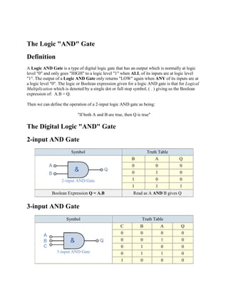
  • 1. The Logic "AND" Gate Definition A Logic AND Gate is a type of digital logic gate that has an output which is normally at logic level "0" and only goes "HIGH" to a logic level "1" when ALL of its inputs are at logic level "1". The output of a Logic AND Gate only returns "LOW" again when ANY of its inputs are at a logic level "0". The logic or Boolean expression given for a logic AND gate is that for Logical Multiplication which is denoted by a single dot or full stop symbol, ( . ) giving us the Boolean expression of: A.B = Q. Then we can define the operation of a 2-input logic AND gate as being: "If both A and B are true, then Q is true" The Digital Logic "AND" Gate 2-input AND Gate Symbol Truth Table B A Q 0 0 0 0 1 0 2-input AND Gate 1 0 0 1 1 1 Boolean Expression Q = A.B Read as A AND B gives Q 3-input AND Gate Symbol Truth Table C B A Q 0 0 0 0 0 0 1 0 0 1 0 0 3-input AND Gate 0 1 1 0 1 0 0 0
  • 2. 1 0 1 0 1 1 0 0 1 1 1 1 Boolean Expression Q = A.B.C Read as A AND B AND C gives Q Because the Boolean expression for the logic AND function is defined as (.), which is a binary operation, AND gates can be cascaded together to form any number of individual inputs. However, commercial available AND gate IC's are only available in standard 2, 3, or 4-input packages. If additional inputs are required, then standard AND gates will need to be cascaded together to obtain the required input value, for example. Multi-input AND Gate The Boolean Expression for this 6-input AND gate will therefore be: Q = (A.B).(C.D).(E.F) The Logic "OR" Gate Definition A Logic OR Gate or Inclusive-OR gate is a type of digital logic gate that has an output which is normally at logic level "0" and only goes "HIGH" to a logic level "1" when one or more of its inputs are at logic level "1". The output, Q of a Logic OR Gate only returns "LOW" again when ALL of its inputs are at a logic level "0". The logic or Boolean expression given for a logic OR gate is that for Logical Addition which is denoted by a plus sign, ( + ) giving us the Boolean expression of: A+B = Q. Then we can define the operation of a 2-input logic OR gate as being:
  • 3. "If either A or B is true, then Q is true" The Digital Logic "OR" Gate 2-input OR Gate Symbol Truth Table B A Q 0 0 0 0 1 1 2-input OR Gate 1 0 1 1 1 1 Boolean Expression Q = A+B Read as A OR B gives Q 3-input OR Gate Symbol Truth Table C B A Q 0 0 0 0 0 0 1 1 0 1 0 1 0 1 1 1 3-input OR Gate 1 0 0 1 1 0 1 1 1 1 0 1 1 1 1 1 Boolean Expression Q = A+B+C Read as A OR B OR C gives Q Like the AND gate, the OR function can have any number of individual inputs. However, commercial available OR gates are available in 2, 3, or 4 inputs types. Additional inputs will require gates to be cascaded together for example. Multi-input OR Gate
  • 4. The Boolean Expression for this 6-input OR gate will therefore be: Q = (A+B)+(C+D)+(E+F) The Digital Logic "NOT" Gate Definition The digital Logic NOT Gate is the most basic of all the logical gates and is sometimes referred to as an Inverting Buffer or simply a Digital Inverter. It is a single input device which has an output level that is normally at logic level "1" and goes "LOW" to a logic level "0" when its single input is at logic level "1", in other words it "inverts" (complements) its input signal. The output from a NOT gate only returns "HIGH" again when its input is at logic level "0" giving us the Boolean expression of: A = Q. Then we can define the operation of a single input logic NOT gate as being: "If A is NOT true, then Q is true" The Digital Inverter or NOT gate Symbol Truth Table A Q 0 1 Inverter or NOT Gate 1 0 Boolean Expression Q = not A or A Read as inverse of A gives Q
  • 5. Logic NOT gates provide the complement of their input signal and are so called because when their input signal is "HIGH" their output state will NOT be "HIGH". Likewise, when their input signal is "LOW" their output state will NOT be "LOW". As they are single input devices, logic NOT gates are not normally classed as "decision" making devices or even as a gate, such as the AND or OR gates which have two or more logic inputs. Commercial available NOT gates IC's are available in either 4 or 6 individual gates within a single i.c. package. The Logic "NAND" Gate Definition The Logic NAND Gate is a combination of the digital logic AND gate with that of an inverter or NOT gate connected together in series. The NAND (Not - AND) gate has an output that is normally at logic level "1" and only goes "LOW" to logic level "0" when ALL of its inputs are at logic level "1". The Logic NAND Gate is the reverse or "Complementary" form of the AND gate we have seen previously. Logic NAND Gate Equivalence The logic or Boolean expression given for a logic NAND gate is that for Logical Addition, which is the opposite to the AND gate, and which it performs on the complements of the inputs. The Boolean expression for a logic NAND gate is denoted by a single dot or full stop symbol, ( . ) with a line or Overline, ( ‾‾ ) over the expression to signify the NOT or logical negation of the NAND gate giving us the Boolean expression of: A.B = Q. The Digital Logic "NAND" Gate 2-input NAND Gate Symbol Truth Table B A Q 0 0 1 0 1 1 2-input NAND Gate 1 0 1 1 1 0
  • 6. Boolean Expression Q = A.B Read as A AND B gives NOT Q 3-input NAND Gate Symbol Truth Table C B A Q 0 0 0 1 0 0 1 1 0 1 0 1 0 1 1 1 3-input NAND Gate 1 0 0 1 1 0 1 1 1 1 0 1 1 1 1 0 Boolean Expression Q = A.B.C Read as A AND B AND C gives NOT Q As with the AND function seen previously, the NAND function can also have any number of individual inputs and commercial available NAND Gate i.c.´s are available in standard 2, 3, or 4 input types The Logic "NOR" Gate Definition The Logic NOR Gate or Inclusive-NOR gate is a combination of the digital logic OR gate with that of an inverter or NOT gate connected together in series. The NOR (Not - OR) gate has an output that is normally at logic level "1" and only goes "LOW" to logic level "0" when ANY of its inputs are at logic level "1". The Logic NOR Gate is the reverse or "Complementary" form of the OR gate we have seen previously. NOR Gate Equivalent The logic or Boolean expression given for a logic NOR gate is that for Logical Multiplication which it performs on the complements of the inputs. The Boolean expression for a logic NOR
  • 7. gate is denoted by a plus sign, ( + ) with a line or Overline, ( ‾‾ ) over the expression to signify the NOT or logical negation of the NOR gate giving us the Boolean expression of: A+B = Q. Then we can define the operation of a 2-input logic NOR gate as being: "If both A and B are NOT true, then Q is true" The Digital Logic "NOR" Gate 2-input NOR Gate Symbol Truth Table B A Q 0 0 1 0 1 0 2-input NOR Gate 1 0 0 1 1 0 Boolean Expression Q = A+B Read as A OR B gives NOT Q 3-input NOR Gate Symbol Truth Table C B A Q 0 0 0 1 0 0 1 0 0 1 0 0 0 1 1 0 3-input NOR Gate 1 0 0 0 1 0 1 0 1 1 0 0 1 1 1 0 Boolean Expression Q = A+B+C Read as A OR B OR C gives NOT Q As with the OR function, the NOR function can also have any number of individual inputs and commercial available NOR Gate IC's are available in standard 2, 3, or 4 input types.
  • 8. The Exclusive-OR Gate Definition Previously, we have seen that for a 2-input OR gate, if A = "1", OR B = "1", OR BOTH A + B = "1" then the output from the gate is also at logic level "1" and this is known as an Inclusive-OR function because it includes the case of Q = "1" when both A and B = "1". If however, an output "1" is obtained ONLY when A = "1" or when B = "1" but NOT both together at the same time, then this type of gate is known as an Exclusive-OR function or an Ex-Or function for short because it excludes the "OR BOTH" case of Q = "1" when both A and B = "1". In other words the output of an Exclusive-OR gate ONLY goes "HIGH" when its two input terminals are at "DIFFERENT" logic levels with respect to each other and they can both be at logic level "1" or both at logic level "0" giving us the Boolean expression of: Q = (A B) = A.B + A.B The Exclusive-OR Gate function is achieved is achieved by combining standard gates together to form more complex gate functions. An example of a 2-input Exclusive-OR gate is given below. The Digital Logic "Ex-OR" Gate 2-input Ex-OR Gate Symbol Truth Table B A Q 0 0 0 0 1 1 2-input Ex-OR Gate 1 0 1 1 1 0 Boolean Expression Q = A B Read as A OR B but NOT BOTH gives Q Then, the logic function implemented by a 2-input Ex-OR is given as "either A OR B but NOT both" will give an output at Q. In general, an Ex-OR gate will give an output value of logic "1" ONLY when there are an ODD number of 1's on the inputs to the gate. Then an Ex-OR function with more than two inputs is called an "odd function" or modulo-2-sum (Mod-2-SUM), not an Ex-OR. This description can be expanded to apply to any number of individual inputs as shown below for a 3-input Ex-OR gate. 3-input Ex-OR Gate
  • 9. Symbol Truth Table C B A Q 0 0 0 0 0 0 1 1 0 1 0 1 0 1 1 0 3-input Ex-OR Gate 1 0 0 1 1 0 1 0 1 1 0 0 1 1 1 1 Boolean Expression Q = A B C Read as "any ODD number of Inputs" gives Q The symbol used to denote an Exclusive-OR function is slightly different to that for the standard Inclusive-OR gate. The logic or Boolean expression given for a logic OR gate is that of logical addition which is denoted by a standard plus sign. The symbol used to describe the Boolean expression for an Exclusive-OR function is a plus sign, ( + ) within a circle, ( Ο ). This exclusive-OR symbol also represents the mathematical "direct sum of sub-objects" expression, with the resulting symbol for an Exclusive-OR function being given as: ( ). We said previously that the Ex-OR function is a combination of different basic logic gates and using the 2-input truth table above, we can expand the Ex-OR function to: Q = (A B) = (A+B).(A.B) which means we can realise this new expression using the following individual gates. SR Flip-Flop The SR flip-flop, also known as a SR Latch, can be considered as one of the most basic sequential logic circuit possible. This simple flip-flop is basically a one-bit memory bistable device that has two inputs, one which will "SET" the device (meaning the output = "1"), and is labelled S and another which will "RESET" the device (meaning the output = "0"), labelled R. Then the SR description stands for "Set-Reset". The reset input resets the flip-flop back to its original state with an output Q that will be either at a logic level "1" or logic "0" depending upon this set/reset condition.
  • 10. A basic NAND gate SR flip-flop circuit provides feedback from both of its outputs back to its opposing inputs and is commonly used in memory circuits to store a single data bit. Then the SR flip-flop actually has three inputs, Set, Reset and its current output Q relating to it's current state or history. The term "Flip-flop" relates to the actual operation of the device, as it can be "flipped" into one logic Set state or "flopped" back into the opposing logic Reset state. The NAND Gate SR Flip-Flop The simplest way to make any basic single bit set-reset SR flip-flop is to connect together a pair of cross-coupled 2-input NAND gates as shown, to form a Set-Reset Bistable also known as an active LOW SR NAND Gate Latch, so that there is feedback from each output to one of the other NAND gate inputs. This device consists of two inputs, one called the Set, S and the other called the Reset, R with two corresponding outputs Q and its inverse or complement Q (not-Q) as shown below. The Basic SR Flip-flop The Set State Consider the circuit shown above. If the input R is at logic level "0" (R = 0) and input S is at logic level "1" (S = 1), the NAND gate Y has at least one of its inputs at logic "0" therefore, its output Q must be at a logic level "1" (NAND Gate principles). Output Q is also fed back to input "A" and so both inputs to NAND gate X are at logic level "1", and therefore its output Q must be at logic level "0". Again NAND gate principals. If the reset input R changes state, and goes HIGH to logic "1" with S remaining HIGH also at logic level "1", NAND gate Y inputs are now R = "1" and B = "0". Since one of its inputs is still at logic level "0" the output at Q still remains HIGH at logic level "1" and there is no change of state. Therefore, the flip-flop circuit is said to be "Latched" or "Set" with Q = "1" and Q = "0". Reset State In this second stable state, Q is at logic level "0", (not Q = "0") its inverse output at Q is at logic level "1", (Q = "1"), and is given by R = "1" and S = "0". As gate X has one of its inputs at logic
  • 11. "0" its output Q must equal logic level "1" (again NAND gate principles). Output Q is fed back to input "B", so both inputs to NAND gate Y are at logic "1", therefore, Q = "0". If the set input, S now changes state to logic "1" with input R remaining at logic "1", output Q still remains LOW at logic level "0" and there is no change of state. Therefore, the flip-flop circuits "Reset" state has also been latched and we can define this "set/reset" action in the following truth table. Truth Table for this Set-Reset Function State S R Q Q Description 1 0 1 0 Set Q » 1 Set 1 1 1 0 no change 0 1 0 1 Reset Q » 0 Reset 1 1 0 1 no change 0 0 0 1 memory with Q = 0 Invalid 0 0 1 0 memory with Q = 1 It can be seen that when both inputs S = "1" and R = "1" the outputs Q and Q can be at either logic level "1" or "0", depending upon the state of inputs S or R BEFORE this input condition existed. However, input state R = "0" and S = "0" is an undesirable or invalid condition and must be avoided because this will give both outputs Q and Q to be at logic level "1" at the same time and we would normally want Q to be the inverse of Q. However, if the two inputs are now switched "HIGH" again after this condition to logic "1", both the outputs will go "LOW" resulting in the flip-flop becoming unstable and switch to an unknown data state based upon the unbalance. This unbalance can cause one of the outputs to switch faster than the other resulting in the flip-flop switching to one state or the other which may not be the required state and data corruption will exist. This unstable condition is known as its Meta-stable state. Then, a bistable SR flip-flop or SR latch is activated or set by a logic "1" applied to its S input and deactivated or reset by a logic "1" applied to its R. The SR flip-flop is said to be in an "invalid" condition (Meta-stable) if both the set and reset inputs are activated simultaneously. The D flip-flop One of the main disadvantages of the basic SR NAND Gate bistable circuit is that the indeterminate input condition of "SET" = logic "0" and "RESET" = logic "0" is forbidden. This state will force both outputs to be at logic "1", over-riding the feedback latching action and whichever input goes to logic level "1" first will lose control, while the other input still at logic "0" controls the resulting state of the latch.
  • 12. But in order to prevent this from happening an inverter can be connected between the "SET" and the "RESET" inputs to produce another type of flip-flop circuit called a Data Latch, Delay flip- flop, D-type Bistable or simply a D-type flip-flop as it is more generally called. The D flip-flop is by far the most important of the clocked flip-flops as it ensures that ensures that inputs S and R are never equal to one at the same time. D-type flip-flops are constructed from a gated SR flip-flop with an inverter added between the S and the R inputs to allow for a single D (data) input. This single data input D is used in place of the "set" signal, and the inverter is used to generate the complementary "reset" input thereby making a level-sensitive D-type flip- flop from a level-sensitive RS-latch as now S = D and R = not D as shown. D flip-flop Circuit We remember that a simple SR flip-flop requires two inputs, one to "SET" the output and one to "RESET" the output. By connecting an inverter (NOT gate) to the SR flip-flop we can "SET" and "RESET" the flip-flop using just one input as now the two input signals are complements of each other. This complement avoids the ambiguity inherent in the SR latch when both inputs are LOW, since that state is no longer possible. Thus the single input is called the "DATA" input. If this data input is HIGH the flip-flop would be "SET" and when it is LOW the flip-flop would be "RESET". However, this would be rather pointless since the flip-flop's output would always change on every data input. To avoid this an additional input called the "CLOCK" or "ENABLE" input is used to isolate the data input from the flip-flop after the desired data has been stored. The effect is that D is only copied to the output Q when the clock is active. This then forms the basis of a D flip-flop. The D flip-flop will store and output whatever logic level is applied to its data terminal so long as the clock input is HIGH. Once the clock input goes LOW the "set" and "reset" inputs of the flip-flop are both held at logic level "1" so it will not change state and store whatever data was present on its output before the clock transition occurred. In other words the output is "latched" at either logic "0" or logic "1". Truth Table for the D Flip-flop
  • 13. Clk D Q Q Description Memory ↓»0 X Q Q no change ↑»1 0 0 1 Reset Q » 0 ↑»1 1 1 0 Set Q » 1 The JK Flip-flop From the previous tutorial we now know that the basic gated SR NAND flip-flop suffers from two basic problems: number one, the S = 0 and R = 0 condition or S = R = 0 must always be avoided, and number two, if S or R change state while the enable input is high the correct latching action may not occur. Then to overcome these two fundamental design problems with the SR flip-flop, the JK flip-Flop was developed. This simple JK flip-Flop is the most widely used of all the flip-flop designs and is considered to be a universal flip-flop circuit. The sequential operation of the JK flip-flop is exactly the same as for the previous SR flip-flop with the same "Set" and "Reset" inputs. The difference this time is that the JK flip-flop has no invalid or forbidden input states of the SR Latch (when S and R are both 1). The JK flip-flop is basically a gated SR flip-flop with the addition of a clock input circuitry that prevents the illegal or invalid output condition that can occur when both inputs S and R are equal to logic level "1". Due to this additional clocked input, a JK flip-flop has four possible input combinations, "logic 1", "logic 0", "no change" and "toggle". The symbol for a JK flip-flop is similar to that of an SR Bistable Latch as seen in the previous tutorial except for the addition of a clock input. The Basic JK Flip-flop
  • 14. Both the S and the R inputs of the previous SR bistable have now been replaced by two inputs called the J and K inputs, respectively after its inventor Jack Kilby. Then this equates to: J = S and K = R. The two 2-input AND gates of the gated SR bistable have now been replaced by two 3-input NAND gates with the third input of each gate connected to the outputs at Q and Q. This cross coupling of the SR flip-flop allows the previously invalid condition of S = "1" and R = "1" state to be used to produce a "toggle action" as the two inputs are now interlocked. If the circuit is now "SET" the J input is inhibited by the "0" status of Q through the lower NAND gate. If the circuit is "RESET" the K input is inhibited by the "0" status of Q through the upper NAND gate. As Q and Q are always different we can use them to control the input. When both inputs J and K are equal to logic "1", the JK flip-flop toggles as shown in the following truth table. The Master-Slave JK Flip-flop The Master-Slave Flip-Flop is basically two gated SR flip-flops connected together in a series configuration with the slave having an inverted clock pulse. The outputs from Q and Q from the "Slave" flip-flop are fed back to the inputs of the "Master" with the outputs of the "Master" flip- flop being connected to the two inputs of the "Slave" flip-flop. This feedback configuration from the slave's output to the master's input gives the characteristic toggle of the JK flip-flop as shown below. The Master-Slave JK Flip-Flop The input signals J and K are connected to the gated "master" SR flip-flop which "locks" the
  • 15. input condition while the clock (Clk) input is "HIGH" at logic level "1". As the clock input of the "slave" flip-flop is the inverse (complement) of the "master" clock input, the "slave" SR flip-flop does not toggle. The outputs from the "master" flip-flop are only "seen" by the gated "slave" flip- flop when the clock input goes "LOW" to logic level "0". When the clock is "LOW", the outputs from the "master" flip-flop are latched and any additional changes to its inputs are ignored. The gated "slave" flip-flop now responds to the state of its inputs passed over by the "master" section. Then on the "Low-to-High" transition of the clock pulse the inputs of the "master" flip-flop are fed through to the gated inputs of the "slave" flip- flop and on the "High-to-Low" transition the same inputs are reflected on the output of the "slave" making this type of flip-flop edge or pulse-triggered. Then, the circuit accepts input data when the clock signal is "HIGH", and passes the data to the output on the falling-edge of the clock signal. In other words, the Master-Slave JK Flip-flop is a "Synchronous" device as it only passes data with the timing of the clock signal. In the next tutorial about Sequential Logic Circuits, we will look at Multivibrators that are used as waveform generators to produce the clock signals to switch sequential circuits. The Shift Register The Shift Register is another type of sequential logic circuit that is used for the storage or transfer of data in the form of binary numbers and then "shifts" the data out once every clock cycle, hence the name "shift register". It basically consists of several single bit "D-Type Data Latches", one for each bit (0 or 1) connected together in a serial or daisy-chain arrangement so that the output from one data latch becomes the input of the next latch and so on. The data bits may be fed in or out of the register serially, i.e. one after the other from either the left or the right direction, or in parallel, i.e. all together. The number of individual data latches required to make up a single Shift Register is determined by the number of bits to be stored with the most common being 8-bits (one byte) wide, i.e. eight individual data latches. The Shift Register is used for data storage or data movement and are used in calculators or computers to store data such as two binary numbers before they are added together, or to convert the data from either a serial to parallel or parallel to serial format. The individual data latches that make up a single shift register are all driven by a common clock ( Clk ) signal making them synchronous devices. Shift register IC's are generally provided with a clear or reset connection so that they can be "SET" or "RESET" as required. Generally, shift registers operate in one of four different modes with the basic movement of data through a shift register being:
  • 16. Serial-in to Parallel-out (SIPO) - the register is loaded with serial data, one bit at a time, with the stored data being available in parallel form. Serial-in to Serial-out (SISO) - the data is shifted serially "IN" and "OUT" of the register, one bit at a time in either a left or right direction under clock control. Parallel-in to Serial-out (PISO) - the parallel data is loaded into the register simultaneously and is shifted out of the register serially one bit at a time under clock control. Parallel-in to Parallel-out (PIPO) - the parallel data is loaded simultaneously into the register, and transferred together to their respective outputs by the same clock pulse. The effect of data movement from left to right through a shift register can be presented graphically as: Also, the directional movement of the data through a shift register can be either to the left, (left shifting) to the right, (right shifting) left-in but right-out, (rotation) or both left and right shifting within the same register thereby making it bidirectional. In this tutorial it is assumed that all the data shifts to the right, (right shifting). Serial-in to Parallel-out (SIPO) 4-bit Serial-in to Parallel-out Shift Register
  • 17. The operation is as follows. Lets assume that all the flip-flops ( FFA to FFD ) have just been RESET ( CLEAR input ) and that all the outputs QA to QD are at logic level "0" i.e, no parallel data output. If a logic "1" is connected to the DATA input pin of FFA then on the first clock pulse the output of FFA and therefore the resulting QA will be set HIGH to logic "1" with all the other outputs still remaining LOW at logic "0". Assume now that the DATA input pin of FFA has returned LOW again to logic "0" giving us one data pulse or 0-1-0. The second clock pulse will change the output of FFA to logic "0" and the output of FFB and QB HIGH to logic "1" as its input D has the logic "1" level on it from QA. The logic "1" has now moved or been "shifted" one place along the register to the right as it is now at QA. When the third clock pulse arrives this logic "1" value moves to the output of FFC ( QC ) and so on until the arrival of the fifth clock pulse which sets all the outputs QA to QD back again to logic level "0" because the input to FFA has remained constant at logic level "0". The effect of each clock pulse is to shift the data contents of each stage one place to the right, and this is shown in the following table until the complete data value of 0-0-0-1 is stored in the register. This data value can now be read directly from the outputs of QA to QD. Then the data has been converted from a serial data input signal to a parallel data output. The truth table and following waveforms show the propagation of the logic "1" through the register from left to right as follows. Basic Movement of Data through a Shift Register Clock Pulse No QA QB QC QD 0 0 0 0 0 1 1 0 0 0 2 0 1 0 0 3 0 0 1 0 4 0 0 0 1 5 0 0 0 0
  • 18. Note that after the fourth clock pulse has ended the 4-bits of data ( 0-0-0-1 ) are stored in the register and will remain there provided clocking of the register has stopped. In practice the input data to the register may consist of various combinations of logic "1" and "0". Commonly available SIPO IC's include the standard 8-bit 74LS164 or the 74LS594. Serial-in to Serial-out (SISO) This shift register is very similar to the SIPO above, except were before the data was read directly in a parallel form from the outputs QA to QD, this time the data is allowed to flow straight through the register and out of the other end. Since there is only one output, the DATA leaves the shift register one bit at a time in a serial pattern, hence the name Serial-in to Serial- Out Shift Register or SISO. The SISO shift register is one of the simplest of the four configurations as it has only three connections, the serial input (SI) which determines what enters the left hand flip-flop, the serial output (SO) which is taken from the output of the right hand flip-flop and the sequencing clock signal (Clk). The logic circuit diagram below shows a generalized serial-in serial-out shift register. 4-bit Serial-in to Serial-out Shift Register
  • 19. You may think what's the point of a SISO shift register if the output data is exactly the same as the input data. Well this type of Shift Register also acts as a temporary storage device or as a time delay device for the data, with the amount of time delay being controlled by the number of stages in the register, 4, 8, 16 etc or by varying the application of the clock pulses. Commonly available IC's include the 74HC595 8-bit Serial-in/Serial-out Shift Register all with 3-state outputs. Parallel-in to Serial-out (PISO) The Parallel-in to Serial-out shift register acts in the opposite way to the serial-in to parallel-out one above. The data is loaded into the register in a parallel format i.e. all the data bits enter their inputs simultaneously, to the parallel input pins PA to PD of the register. The data is then read out sequentially in the normal shift-right mode from the register at Q representing the data present at PA to PD. This data is outputted one bit at a time on each clock cycle in a serial format. It is important to note that with this system a clock pulse is not required to parallel load the register as it is already present, but four clock pulses are required to unload the data. 4-bit Parallel-in to Serial-out Shift Register As this type of shift register converts parallel data, such as an 8-bit data word into serial format, it can be used to multiplex many different input lines into a single serial DATA stream which can be sent directly to a computer or transmitted over a communications line. Commonly available IC's include the 74HC166 8-bit Parallel-in/Serial-out Shift Registers.
  • 20. Parallel-in to Parallel-out (PIPO) The final mode of operation is the Parallel-in to Parallel-out Shift Register. This type of register also acts as a temporary storage device or as a time delay device similar to the SISO configuration above. The data is presented in a parallel format to the parallel input pins PA to PD and then transferred together directly to their respective output pins QA to QA by the same clock pulse. Then one clock pulse loads and unloads the register. This arrangement for parallel loading and unloading is shown below. 4-bit Parallel-in to Parallel-out Shift Register The PIPO shift register is the simplest of the four configurations as it has only three connections, the parallel input (PI) which determines what enters the flip-flop, the parallel output (PO) and the sequencing clock signal (Clk). Similar to the Serial-in to Serial-out shift register, this type of register also acts as a temporary storage device or as a time delay device, with the amount of time delay being varied by the frequency of the clock pulses. Also, in this type of register there are no interconnections between the individual flip-flops since no serial shifting of the data is required. Asynchronous Counter
  • 21. In the previous tutorial we saw that an Asynchronous counter can have 2n-1 possible counting states e.g. MOD-16 for a 4-bit counter, (0-15) making it ideal for use in Frequency Division. But it is also possible to use the basic asynchronous counter to construct special counters with counting states less than their maximum output number by forcing the counter to reset itself to zero at a pre-determined value producing a type of asynchronous counter that has truncated sequences. Then an n-bit counter that counts up to its maximum modulus (2n) is called a full sequence counter and a n-bit counter whose modulus is less than the maximum possible is called a truncated counter. But why would we want to create an asynchronous truncated counter that is not a MOD-4, MOD-8, or some other modulus that is equal to the power of two. The answer is that we can by using combinational logic to take advantage of the asynchronous inputs on the flip-flop. If we take the modulo-16 asynchronous counter and modified it with additional logic gates it can be made to give a decade (divide-by-10) counter output for use in standard decimal counting and arithmetic circuits. Such counters are generally referred to as Decade Counters. A decade counter requires resetting to zero when the output count reaches the decimal value of 10, ie. when DCBA = 1010 and to do this we need to feed this condition back to the reset input. A counter with a count sequence from binary "0000" (BCD = "0") through to "1001" (BCD = "9") is generally referred to as a BCD binary-coded-decimal counter because its ten state sequence is that of a BCD code but binary decade counters are more common. Asynchronous Decade Counter This type of asynchronous counter counts upwards on each leading edge of the input clock signal starting from "0000" until it reaches an output "1010" (decimal 10). Both outputs QB and QD are now equal to logic "1" and the output from the NAND gate changes state from logic "1" to a logic "0" level and whose output is also connected to the CLEAR (CLR) inputs of all the J-K Flip-flops.
  • 22. This signal causes all of the Q outputs to be reset back to binary "0000" on the count of 10. Once QB and QD are both equal to logic "0" the output of the NAND gate returns back to a logic level "1" and the counter restarts again from "0000". We now have a decade or Modulo-10 counter. Decade Counter Truth Table Clock Output bit Pattern Decimal Count QD QC QB QA Value 1 0 0 0 0 0 2 0 0 0 1 1 3 0 0 1 0 2 4 0 0 1 1 3 5 0 1 0 0 4 6 0 1 0 1 5 7 0 1 1 0 6 8 0 1 1 1 7 9 1 0 0 0 8 10 1 0 0 1 9 11 Counter Resets its Outputs back to Zero Decade Counter Timing Diagram Using the same idea of truncating counter output sequences, the above circuit could easily be
  • 23. adapted to other counting cycles be simply changing the connections to the AND gate. For example, a scale-of-twelve (modulo-12) can easily be made by simply taking the inputs to the AND gate from the outputs at "QC" and "QD", noting that the binary equivalent of 12 is "1100" and that output "QA" is the least significant bit (LSB). Since the maximum modulus that can be implemented with n flip-flops is 2n, this means that when you are designing truncated asynchronous counters you should determine the lowest power of two that is greater than or equal to your desired modulus. For example, lets say you wish to count from 0 to 39, or mod-40. Then the highest number of flip-flops required would be six, n = 6 giving a maximum MOD of 64 as five flip-flops would only equal MOD-32. Now suppose we wanted to build a "divide-by-128" counter for frequency division we would need to cascade seven flip-flops since 128 = 27. Using dual flip-flops such as the 74LS74 we would still need four IC's to complete the circuit. One easy alternative method would be to use two TTL 7493's as 4-bit ripple counter/dividers. Since 128 = 16 x 8, one 7493 could be configured as a "divide-by-16" counter and the other as a "divide-by-8" counter. The two IC's would be cascaded together to form a "divide-by-128" frequency divider as shown. Of course standard IC asynchronous counters are available such as the TTL 74LS90 programmable ripple counter/divider which can be configured as a divide-by-2, divide-by-5 or any combination of both. The 74LS390 is a very flexible dual decade driver IC with a large number of "divide-by" combinations available ranging form divide-by-2, 4, 5, 10, 20, 25, 50, and 100 Binary Synchronous Counter In the previous Asynchronous binary counter tutorial, we saw that the output of one counter stage is connected directly to the clock input of the next counter stage and so on along the chain, and as a result the asynchronous counter suffers from what is known as "Propagation Delay" in which the timing signal is delayed a fraction through each flip-flop. However, with the Synchronous Counter, the external clock signal is connected to the clock input of EVERY individual flip-flop within the counter so that all of the flip-flops are clocked together simultaneously (in parallel) at the same time giving a fixed time relationship. In other words, changes in the output occur in "synchronization" with the clock signal. This results in all the individual output bits changing state at exactly the same time in response to the common clock signal with no ripple effect and therefore, no propagation delay. Binary 4-bit Synchronous Counter
  • 24. It can be seen that the external clock pulses (pulses to be counted) are fed directly to each J-K flip-flop in the counter chain and that both the J and K inputs are all tied together in toggle mode, but only in the first flip-flop, flip-flop A (LSB) are they connected HIGH, logic "1" allowing the flip-flop to toggle on every clock pulse. Then the synchronous counter follows a predetermined sequence of states in response to the common clock signal, advancing one state for each pulse. The J and K inputs of flip-flop B are connected to the output "Q" of flip-flop A, but the J and K inputs of flip-flops C and D are driven from AND gates which are also supplied with signals from the input and output of the previous stage. If we enable each J-K flip-flop to toggle based on whether or not all preceding flip-flop outputs (Q) are "HIGH" we can obtain the same counting sequence as with the asynchronous circuit but without the ripple effect, since each flip- flop in this circuit will be clocked at exactly the same time. As there is no propagation delay in synchronous counters because all the counter stages are triggered in parallel the maximum operating frequency of this type of counter is much higher than that of a similar asynchronous counter. 4-bit Synchronous Counter Waveform Timing Diagram.
  • 25. Because this 4-bit synchronous counter counts sequentially on every clock pulse the resulting outputs count upwards from 0 ( "0000" ) to 15 ( "1111" ). Therefore, this type of counter is also known as a 4-bit Synchronous Up Counter. As synchronous counters are formed by connecting flip-flops together and any number of flip- flops can be connected or "cascaded" together to form a "divide-by-n" binary counter, the modulo's or "MOD" number still applies as it does for asynchronous counters so a Decade counter or BCD counter with counts from 0 to 2n-1 can be built along with truncated sequences. Combinational Logic Circuits Unlike Sequential Logic Circuits whose outputs are dependant on both their present inputs and their previous output state giving them some form of Memory, the outputs of Combinational Logic Circuits are only determined by the logical function of their current input state, logic "0" or logic "1", at any given instant in time as they have no feedback, and any changes to the signals being applied to their inputs will immediately have an effect at the output. In other words, in a Combinational Logic Circuit, the output is dependant at all times on the combination of its inputs and if one of its inputs condition changes state so does the output as combinational circuits have "no memory", "timing" or "feedback loops". Combinational Logic
  • 26. Combinational Logic Circuits are made up from basic logic NAND, NOR or NOT gates that are "combined" or connected together to produce more complicated switching circuits. These logic gates are the building blocks of combinational logic circuits. An example of a combinational circuit is a decoder, which converts the binary code data present at its input into a number of different output lines, one at a time producing an equivalent decimal code at its output. Combinational logic circuits can be very simple or very complicated and any combinational circuit can be implemented with only NAND and NOR gates as these are classed as "universal" gates. The three main ways of specifying the function of a combinational logic circuit are: 1. Boolean Algebra – This forms the algebraic expression showing the operation of the logic circuit for each input variable either True or False that results in a logic "1" output. 2. Truth Table – A truth table defines the function of a logic gate by providing a concise list that shows all the output states in tabular form for each possible combination of input variable that the gate could encounter. 3. Logic Diagram – This is a graphical representation of a logic circuit that shows the wiring and connections of each individual logic gate, represented by a specific graphical symbol, that implements the logic circuit. and all three of these logic circuit representations are shown below.
  • 27. As combinational logic circuits are made up from individual logic gates only, they can also be considered as "decision making circuits" and combinational logic is about combining logic gates together to process two or more signals in order to produce at least one output signal according to the logical function of each logic gate. Common combinational circuits made up from individual logic gates that carry out a desired application include Multiplexers, De- multiplexers, Encoders, Decoders, Full and Half Adders etc. Classification of Combinational Logic One of the most common uses of combinational logic is in Multiplexer and De-multiplexer type circuits. Here, multiple inputs or outputs are connected to a common signal line and logic gates
  • 28. are used to decode an address to select a single data input or output switch. A multiplexer consist of two separate components, a logic decoder and some solid state switches, but before we can discuss multiplexers, decoders and de-multiplexers in more detail we first need to understand how these devices use these "solid state switches" in their design. The Half Adder Circuit Another common and very useful combinational logic circuit which can be constructed using just a few basic logic gates and adds together binary numbers is the Binary Adder circuit. The Binary Adder is made up from standard AND and Ex-OR gates and allow us to "add" together single bit binary numbers, a and b to produce two outputs called the SUM of the addition and a CARRY called the Carry-out, ( C out ) bit. One of the main uses for the Binary Adder is in arithmetic and counting circuits. Consider the addition of two denary (base 10) numbers below. 123 A (Augend) + 789 B (Addend) 912 SUM Each column is added together starting from the right hand side and each digit has a weighted value depending upon its position in the columns. As each column is added together a carry is generated if the result is greater or equal to ten, the base number. This carry is then added to the result of the addition of the next column to the left and so on, simple school math's addition. The adding of binary numbers is basically the same as that of adding decimal numbers but this time a carry is only generated when the result in any column is greater or equal to "2", the base number of binary. 1-bit Adder with Carry-Out Symbol Truth Table A B SUM CARRY 0 0 0 0 0 1 1 0 1 0 1 0 1 1 0 1 Boolean Expression: Sum = A ⊕ B Carry = A . B
  • 29. From the truth table we can see that the SUM (S) output is the result of the Ex-OR gate and the Carry-out (Cout) is the result of the AND gate. One major disadvantage of the Half Adder circuit when used as a binary adder, is that there is no provision for a "Carry-in" from the previous circuit when adding together multiple data bits. For example, suppose we want to add together two 8-bit bytes of data, any resulting carry bit would need to be able to "ripple" or move across the bit patterns starting from the least significant bit (LSB). The most complicated operation the half adder can do is "1 + 1" but as the half adder has no carry input the resultant added value would be incorrect. One simple way to overcome this problem is to use a Full Adder type binary adder circuit. The Full Adder Circuit The main difference between the Full Adder and the previous seen Half Adder is that a full adder has three inputs, the same two single bit binary inputs A and B as before plus an additional Carry-In (C-in) input as shown below. Full Adder with Carry-In Symbol Truth Table A B C-in Sum C-out 0 0 0 0 0 0 1 0 1 0 1 0 0 1 0 1 1 0 0 1 0 0 1 1 0 0 1 1 0 1 1 0 1 0 1 1 1 1 1 1 Boolean Expression: Sum = A ⊕ B ⊕ C-in The 1-bit Full Adder circuit above is basically two half adders connected together and consists of three Ex-OR gates, two AND gates and an OR gate, six logic gates in total. The truth table for the full adder includes an additional column to take into account the Carry-in input as well as the summed output and carry-output. 4-bit full adder circuits are available as standard IC packages in the form of the TTL 74LS83 or the 74LS283 which can add together two 4-bit binary numbers and generate a SUM and a CARRY output. But what if we wanted to add together two n-bit numbers, then n 1-bit full adders need to be connected together to produce what is known as the Ripple Carry Adder.
  • 30. The 4-bit Binary Adder The Ripple Carry Binary Adder is simply n, full adders cascaded together with each full adder represents a single weighted column in the long addition with the carry signals producing a "ripple" effect through the binary adder from right to left. For example, suppose we want to "add" together two 4-bit numbers, the two outputs of the first full adder will provide the first place digit sum of the addition plus a carry-out bit that acts as the carry-in digit of the next binary adder. The second binary adder in the chain also produces a summed output (the 2nd bit) plus another carry-out bit and we can keep adding more full adders to the combination to add larger numbers, linking the carry bit output from the first full binary adder to the next full adder, and so forth. An example of a 4-bit adder is given below. A 4-bit Binary Adder One main disadvantage of "cascading" together 1-bit binary adders to add large binary numbers is that if inputs A and B change, the sum at its output will not be valid until any carry-input has "rippled" through every full adder in the chain. Consequently, there will be a finite delay before the output of a adder responds to a change in its inputs resulting in the accumulated delay especially in large multi-bit binary adders becoming prohibitively large. This delay is called Propagation delay. Also "overflow" occurs when an n-bit adder adds two numbers together whose sum is greater than or equal to 2n One solution is to generate the carry-input signals directly from the A and B inputs rather than using the ripple arrangement above. This then produces another type of binary adder circuit called a Carry Look Ahead Binary Adder were the speed of the parallel adder can be greatly improved using carry-look ahead logic.