SlideShare una empresa de Scribd logo
1 de 15
Atomic Structure
The atom is basically composed of electrons, protons, and neutrons. The electrons, protons, and neutrons of one element are
identical to those of any other element. There are different kinds of elements because the number and the arrangement of
electrons and protons are different for each element.
The electron carries a small negative charge of electricity. The proton carries a positive charge of electricity equal and opposite to
the charge of the electron. Both the electron and proton have the same quantity of charge, although the mass of the proton is
approximately 1,827 times that of the electron. In some atoms there exists a neutral particle called a neutron. The neutron has a
mass approximately equal to that of a proton, but it has no electrical charge.
According to theory, the electrons, protons, and neutrons of the atoms are thought to be arranged in a manner similar to a
miniature solar system. Notice the helium atom in the figure. Two protons and two neutrons form the heavy nucleus with a positive
charge around which two very light electrons revolve. The path each electron takes around the nucleus is called an orbit. The
electrons are continuously being acted upon in their orbits by the force of attraction of the nucleus. To maintain an orbit around the
nucleus, the electrons travel at a speed that produces a counterforce equal to the attraction force of the nucleus. Just as energy is
required to move a space vehicle away from the earth, energy is also required to move an electron away from the nucleus. Like a
space vehicle, the electron is said to be at a higher energy level when it travels a larger orbit. Scientific experiments have shown
that the electron requires a certain amount of energy to stay in orbit. This quantity is called the electron's energy level. By virtue of
just its motion alone, the electron contains kinetic energy. Because of its position, it also contains potential energy. The total
energy contained by an electron (kinetic energy plus potential energy) is the main factor that determines the radius of the
electron's orbit. For an electron to remain in this orbit, it must neither gain nor lose energy.
The orbiting electrons do not follow random paths, instead they are confined to definite energy levels. Visualize these levels as
shells with each successive shell being spaced a greater distance from the nucleus. The shells, and the number of electrons
required to fill them, may be predicted by using Pauli's exclusion principle:
K-shell 2 electrons (n=1)
L-shell 8 electrons (n=2)
M-shell 18 electrons (n=3)
N-shell 32 electrons (n=4)
Table 1: The number of electrons required to fill the shells
Simply stated, this principle specifies that each shell will contain a maximum of 2·n2
electrons, where n corresponds to the shell
number starting with the one closest to the nucleus. By this principle, the second shell, for example, would contain 2·22
or 8
electrons when full. A list of all the other known elements, with the number of electrons in each atom, is contained in the Periodic
Table of Elements. This periodic table of elements can be explanated physically with help of the „Bohr-Sommerfeld” theory of
atomic structure.
Energy Bands
Orbiting electrons contain energy and are confined to definite energy levels. The various shells in an atom represent these levels.
Therefore, to move an electron from a lower shell to a higher shell a certain amount of energy is required. This energy can be in
the form of electric fields, heat, light, and even bombardment by other particles. Failure to provide enough energy to the electron,
even if the energy supplied is just short of the required amount, will cause it to remain at its present energy level. Supplying more
energy than is needed will only cause the electron to move to the next higher shell and the remaining energy will be wasted. In
simple terms, energy is required in definite units to move electrons from one shell to the next higher shell. These units are
calledquanta (for example 1, 2, or 3 quanta).
Electrons can also lose energy as well as receive it. When an electron loses energy, it moves to a lower shell. The lost energy, in
some cases, appears as heat. If a sufficient amount of energy is absorbed by an electron, it is possible for that electron to be
completely removed from the influence of the atom. This is calledionization. When an atom loses electrons or gains electrons in
this process of electron exchange, it is said to be ionized. For ionization to take place, there must be a transfer of energy that
results in a change in the internal energy of the atom. An atom having more than its normal amount of electrons acquires a
negative charge, and is called a negative ion. The atom that gives up some of its normal electrons is left with fewer negative
charges than positive charges and is called a positive ion. Thus, we can define ionization as the process by which an atom loses
or gains electrons.
Up to this point, we have spoken only of isolated atoms. When atoms are spaced far enough apart, as in a gas, they have very
little influence upon each other, and are very much like lone atoms. But atoms within a solid have a marked effect upon each
other. The forces that bind these atoms together greatly modify the behavior of the other electrons. One consequence of this close
proximity of atoms is to cause the individual energy levels of an atom to break up and form bands of energy. Discrete (separate
and complete) energy levels still exist within these energy bands, but there are many more energy levels than there were with the
isolated atom. In some cases, energy levels will have disappeared. Figure 3 shows the difference in the energy arrangement
between an isolated atom and the atom in a solid. Notice that the isolated atom (such as in gas) has energy levels, whereas the
atom in a solid has energy levels grouped into Energy Bands.
The upper band in the solid lines in figure 3 is called the conduction band because electrons in this band are easily removed by
the application of external electric fields. Materials that have a large number of electrons in the conduction band act as good
conductors of electricity.
Below the conduction band is the forbidden band or energy gap. Electrons are never found in this band, but may travel back and
forth through it, provided they do not come to rest in the band.
The last band or valence band is composed of a series of energy levels containing valence electrons. Electrons in this band are
more tightly bound to the individual atom than the electrons in the conduction band. However, the electrons in the valence band
can still be moved to the conduction band with the application of energy, usually thermal energy. There are more bands below the
valence band, but they are not important to the understanding of semiconductor theory and will not be discussed.
The concept of energy bands is particularly important in classifying materials as conductors, semiconductors, and insulators. An
electron can exist in either of two energy bands, the conduction band or the valence band. All that is necessary to move an
electron from the valence band to the conduction band so it can be used for electric current, is enough energy to carry the electron
through the forbidden band. The width of the forbidden band or the separation between the conduction and valence bands
determines whether a substance is an insulator, semiconductor, or conductor. Figure 4 uses energy level diagrams to show the
difference between insulators, semiconductors, and conductors.
The energy diagram for the insulator shows the insulator with a very wide energy gap. The wider this gap, the greater the amount
of energy required to move the electron from the valence band to the conduction band. Therefore, an insulator requires a large
amount of energy to obtain a small amount of current. The insulator „insulates” because of the wide forbidden band or energy gap.
The semiconductor, on the other hand, has a smaller forbidden band and requires less energy to move an electron from the
valence band to the conduction band. Therefore, for a certain amount of applied voltage, more current will flow in the
semiconductor than in the insulator.
The last energy level diagram in figure 4 is that of a conductor. Notice, there is no forbidden band or energy gap and the valence
and conduction bands overlap. With no energy gap, it takes a small amount of energy to move electrons into the conduction band;
consequently, conductors pass electrons very easily.
Covalent Bonding:
The chemical activity of an atom is determined by the number of electrons in its valence shell. When the valence shell is complete,
the atom is stable and shows little tendency to combine with other atoms to form solids. Only atoms that possess eight valence
electrons have a complete outer shell. These atoms are referred to as inert or inactive atoms. However, if the valence shell of an
atom lacks the required number of electrons to complete the shell, then the activity of the atom increases.
Silicon and germanium, for example, are the most frequently used semiconductors. Both are quite similar in their structure and
chemical behavior. Each has four electrons in the valence shell. Consider just germanium. Since it has fewer than the required
number of eight electrons needed in the outer shell, its atoms will unite with other atoms until eight electrons are shared. This
gives each atom a total of eight electrons in its valence shell; four of its own and four that it borrowed from the surrounding atoms.
The sharing of valence electrons between two or more atoms produces a covalent bond between the atoms. It is this bond that
holds the atoms together in an orderly structure called a crystal. A crystal is just another name for a solid whose atoms or
molecules are arranged in a three-dimensional geometrical pattern commonly referred to as a lattice. Figure 1 shows a typical
crystal structure. Each sphere in the figure represents the nucleus of an atom, and the arms that join the atoms and support the
structure are the covalent bonds.
As a result of this sharing process, the valence electrons are held tightly together. This can best be illustrated by the two-
dimensional view of the germanium lattice in figure 2. The big circles in the figure represent the nuclei of the atoms. The small
circles indicate valence electrons. Because every atom in this pattern is bonded to four other atoms, the electrons are not free to
move within the crystal. As a result of this bonding, pure germanium and silicon are poor conductors of electricity. The reason they
are not insulators but semiconductors is that with the proper application of heat or electrical pressure, electrons can be caused to
break free of their bonds and move into the conduction band. Once in this band, they wander aimlessly through the crystal.
Conduction Process
As stated earlier, energy can be added to electrons by applying heat. When enough energy is absorbed by the valence electrons,
it is possible for them to break some of their covalent bonds. Once the bonds are broken, the electrons move to the conduction
band where they are capable of supporting electric current. When a voltage is applied to a crystal containing these conduction
band electrons, the electrons move through the crystal toward the applied voltage. This movement of electrons in a semiconductor
is referred to as electron current flow.
There is still another type of current in a pure semiconductor. This current occurs when a covalent bond is broken and a vacancy
is left in the atom by the missing valence electron. This vacancy is commonly referred to as a „hole”. The hole is considered to
have a positive charge because its atom is deficient by one electron, which causes the protons to outnumber the electrons. As a
result of this hole, a chain reaction begins when a nearby electron breaks its own covalent bond to fill the hole, leaving another
hole. Then another electron breaks its bond to fill the previous hole, leaving still another hole. Each time an electron in this
process fills a hole, it enters into a covalent bond.
Even though an electron has moved from one covalent bond to
another, the most important thing to remember is that the hole is also moving.
Therefore, since this process of conduction resembles the movement of holes
rather than electrons, it is termed hole flow (short for hole current flow or
conduction by holes). Hole flow is very similar to electron flow except that the
holes move toward a negative potential and in an opposite direction to that of
the electron. Since hole flow results from the breaking of covalent bonds,
which are at the valence band level, the electrons associated with this type of
conduction contain only valence band energy and must remain in the valence
band. However, the electrons associated with electron flow have conduction
band energy and can, therefore, move throughout the crystal. A good analogy
of hole flow is the movement of a hole through a plank with drill holes filled with balls (figure 1).
When a ball is removed from the plank, a hole is left. This hole is then filled by the ball number 2, which leaves still another hole.
Ball number 3 then moves into the hole left by ball number 2. This causes still another hole to appear where ball 3 was. Notice the
holes are moving to the left side of the plank. This action continues until all the balls have moved one space to the right in which
time the hole moved four spaces to the left and came to rest at the left-hand end of the plank.
In the theory just described, two current carriers were created by the breaking of covalent bonds: the negative electron and the
positive hole. These carriers are referred to as electron-hole pairs. Since the semiconductor we have been discussing contains no
impurities, the number of holes in the electron-hole pairs is always equal to the number of conduction electrons. Another way of
describing this condition where no impurities exist is by saying the semiconductor is intrinsic. The term intrinsic is also used to
distinguish the pure semiconductor that we have been working with from one containing impurities.
Doping Process
The pure semiconductor mentioned earlier is basically neutral. It contains no free electrons in its conduction bands. Even with the
application of thermal energy, only a few covalent bonds are broken, yielding a relatively small current flow. A much more efficient
method of increasing current flow in semiconductors is by adding very small amounts of selected additives to them, generally no
more than a few parts per million. These additives are called impurities and the process of adding them to crystals is referred to
as doping. The purpose of semiconductor doping is to increase the number of free charges that can be moved by an external
applied voltage. When an impurity increases the number of free electrons, the doped semiconductor is negative or n-type, and the
impurity that is added is known as an n-typeimpurity. However, an impurity that reduces the number of free electrons, causing
more holes, creates a positive or p-type semiconductor, and the impurity that was added to it is known as a p-type impurity.
Semiconductors which are doped in this manner - either with n- or p-type impurities - are referred to as extrinsicsemiconductors.
i) n-Type Semiconductor
The n-type impurity loses its extra valence electron easily when added to a
semiconductor material, and in so doing, increases the conductivity of the
material by contributing a free electron. This type of impurity has 5 valence
electrons and is called a pentavalent impurity. Arsenic, antimony, bismuth,
and phosphorous are pentavalent impurities. Because these materials give
or donate one electron to the doped material, they are also
called donor impurities.
When a pentavalent (donor) impurity, like arsenic, is added to germanium, it
will form covalent bonds with the germanium atoms. Figure 1 illustrates this
by showing an arsenic atom (As) in a germanium (Ge) lattice structure. Notice the arsenic atom in the center of the lattice. It has
5 valence electrons in its outer shell but uses only 4 of them to form covalent bonds with the germanium atoms, leaving 1 electron
relatively free in the crystal structure. Pure germanium may be converted into an n-type semiconductor by „doping” it with any
donor impurity having 5 valence electrons in its outer shell. Since this type of semiconductor (n-type) has a surplus of electrons,
the electrons are considered majority carriers, while the holes, being few in number, are the minority carriers.
Conduction in the n-type semiconductor, or crystal, is similar to conduction in a copper wire. That is, with voltage applied across
the material, electrons will move through the crystal just as current would flow in a copper wire. The positive potential of a battery
will attract the free electrons in the crystal. These electrons will leave the crystal and flow into the positive terminal of the battery.
As an electron leaves the crystal, an electron from the negative terminal of the battery will enter the crystal, thus completing the
current path. Therefore, the majority current carriers in the n-type material (electrons) are repelled by the negative side of the
battery and move through the crystal toward the positive side of the battery.
ii) p-Type Semiconductor:
The second type of impurity, when added to a
semiconductor material, tends to compensate for its deficiency of
1 valence electron by acquiring an electron from its neighbor.
Impurities of this type have only 3 valence electrons and are
called trivalent impurities. Aluminum, indium, gallium, and boron
are trivalent impurities. Because these materials accept 1 electron
from the doped material, they are also called acceptor impurities.
A trivalent (acceptor) impurity element can also be used
to dope germanium. In this case, the impurity is 1 electron short
of the required amount of electrons needed to establish covalent
bonds with 4 neighboring atoms. Thus, in a single covalent bond,
there will be only 1 electron instead of 2. This arrangement leaves a hole in that covalent bond. Figure 2 illustrates
this theory by showing what happens when germanium is doped with an indium (In) atom. Notice, the indium atom
in the figure is 1 electron short of the required amount of electrons needed to form covalent bonds with
4 neighboring atoms and, therefore, creates a hole in the structure. Gallium and boron, which are also trivalent
impurities, exhibit these same characteristics when added to germanium. The holes can only be present in this type
semiconductor when a trivalent impurity is used. Note that a hole carrier is not created by the removal of an electron
from a neutral atom, but is created when a trivalent impurity enters into covalent bonds with a tetravalent (4 valence
electrons) crystal structure. The holes in this type of semiconductor (p-type) are considered the majority carriers
since they are present in the material in the greatest quantity. The electrons, on the other hand, are the minority
carriers.
Current Flow in the p-type Material is by positive holes, instead of negative electrons. A hole moves from
the positive terminal of the p-material to the negative terminal. Electrons from the external circuit enter the negative
terminal of the material and fill holes in the vicinity of this terminal. At the positive terminal, electrons are removed
from the covalent bonds, thus creating new holes. This process continues as the steady stream of holes (hole
current) moves toward the negative terminal.
Notice in both n-type and p-type materials, current flow in the external circuit consists of electrons moving out of the
negative terminal of the battery and into the positive terminal of the battery. Hole flow, on the other hand, only exists
within the material itself.
Semiconductor Diode
If we join a section of n-type semiconductor material with a similar
section of p-type semiconductor material, we obtain a device known as
a pn junction. (The area where the n and p regions meet is appropriately called
the junction.) The usual characteristics of this device make it extremely useful in
electronics as a diode rectifier. The diode is nothing more than a two-element
semiconductor device that makes use of the rectifying properties of a pn junction
to convert alternating current into direct current by permitting current flow in only
one direction. The schematic symbol of a pn junction diode is shown in figure 1.
The horizontal bar represents the cathode (n-type material) since it is the
source of electrons and the arrow represents the anode (p-type material) since
it is the destination of the electrons. (Notice the electron flow is against the
arrow.) The label „CR1” is an alphanumerical code used to identify the diode. In
this figure, we have only one diode so it is labeled CR1 (crystal rectifier number one).
Junction Barrier
Although the n-type material has an excess of free electrons, it is still electrically neutral. This is because the donor atoms
in the n material were left with positive charges after free electrons became available by covalent bonding (the protons outnumbered
the electrons). Therefore, for every free electron in the n material, there is a corresponding positively charge atom to balance it. The
end result is that the p material has an overall charge of zero.
By the same reasoning, the p-type material is also electrically neutral because the excess of holes in this material is exactly
balanced by the number of electrons. Keep in mind that the holes and electrons are still free to move in the material because they
are only loosely bound to their parent atoms.
It would seem that if we joined the n and p materials together by one of the
processes mentioned earlier, all the holes and electrons would pair up. On the
contrary, this does not happen. Instead the electrons in then material diffuse (move
or spread out) across the junction into the p material and fill some of the holes. At
the same time, the holes in the p material diffuse across the junction into
the n material and are filled byn material electrons. This process, called junction
recombination, reduces the number of free electrons and holes in the vicinity of the
junction. Because there is a depletion, or lack of free electrons and holes in this
area, it is known as the depletion region.
The loss of an electron from the n-type material created a positive ion in
the n material, while the loss of a hole from the p material created a negative ion in
that material. These ions are fixed in place in the crystal lattice structure and cannot
move. Thus, they make up a layer of fixed charges on the two sides of the junction
as shown in figure 2. On the n side of the junction, there is a layer of positively
charged ions; on thep side of the junction, there is a layer of negatively charged ions.
An electrostatic field is established across the junction between the oppositely
charged ions. The diffusion of electrons and holes across the junction will continue
until the magnitude of the electrostatic field is increased to the point where the
electrons and holes no longer have enough energy to overcome it, and are repelled
by the negative and positive ions respectively. At this point equilibrium is established
and, for all practical purposes, the movement of carriers across the junction ceases.
For this reason, the electrostatic field created by the positive and negative ions in the
depletion region is called a barrier.
The action just described occurs almost instantly when the junction is formed. Only the carriers in the immediate vicinity
of the junction are affected. The carriers throughout the remainder of the n and p material are relatively undisturbed and remain in
a balanced condition.
Forward Bias
An external voltage applied to a pn junction is called bias. If, for example, a battery is used to supply bias to apn junction and is
connected so that its voltage opposes the junction field, it will reduce the junction barrier and, therefore, aid current flow through
the junction. This type of bias is known as forward bias, and it causes the junction to offer only minimum resistance to the flow of
current.
The positive potential connected to the p-type material repels holes toward the
junction where they neutralize some of the negative ions. At the same time the
negative potential connected to the n-type material repels electrons toward the
junction where they neutralize some of the positive ions. Since ions on both
sides of the barrier are being neutralized, the width of the barrier decreases.
Thus, the effect of the battery voltage in the forward-bias direction is to reduce
the barrier potential across the junction and to allow majority carriers to cross the
junction. Current flow in the forward-biased pn junction is relatively simple. An
electron leaves the negative terminal of the battery and moves to the terminal of
the n-type material. It enters the n material, where it is the majority carrier and
moves to the edge of the junction barrier. Because of forward bias, the barrier offers less opposition to the electron and it will pass
through the depletion region into the p-type material. The electron loses energy in overcoming the opposition of the junction
barrier, and upon entering the p material, combines with a hole. The hole was produced when an electron was extracted from
the p material by the positive potential of the battery. The created hole moves through the p material toward the junction where it
combines with an electron.
It is important to remember that increasing the battery voltage will increase the number of majority carriers arriving at the junction
and will therefore increase the current flow. If the battery voltage is increased to the point where the barrier is greatly reduced, a
heavy current will flow and the junction may be damaged from the resulting heat.
Reverse Bias
If the battery mentioned earlier is connected across the junction so that its voltage aids
the junction, it will increase the junction barrier and thereby offer a high resistance to the
current flow through the junction. This type of bias is known as reverse bias.
To reverse bias a junction diode, the negative battery terminal is connected to the p-
type material, and the positive battery terminal to the n-type material as shown in figure
4. The negative potential attracts the holes away from the edge of the junction barrier on
the p side, while the positive potential attracts the electrons away from the edge of the
barrier on the n side. This action increases the barrier width because there are more
negative ions on the p side of the junction, and more positive ions on the n side of the
junction. Notice in the figure the width of the barrier has increased. This increase in the number of ions prevents current flow
across the junction by majority carriers. However, the current flow across the barrier is not quite zero because of the minority
carriers crossing the junction. As you recall, when the crystal is subjected to an external source of energy (light, heat, etc.),
electron-hole pairs are generated. The electron-hole pairs produce minority current carriers. There are minority current carriers in
both regions: holes in the n material and electrons in the n material. With reverse bias, the electrons in the p-type material are
repelled toward the junction by the negative terminal of the battery.
As the electron moves across the junction, it will neutralize a positive ion in
the n-type material. Similarly, the holes in the n-type material will be repelled by the
positive terminal of the battery toward the junction. As the hole crosses the junction,
it will neutralize a negative ion in the p-typematerial.This movement of minority
carriers is called minority current flow, because the holes and electrons involved
come from the electron-hole pairs that are generated in the crystal lattice structure,
and not from the addition of impurity atoms.
Therefore, when a pn junction is reverse biased, there will be no current flow
because of majority carriers but a very small amount of current because of minority
carriers crossing the junction. However, at normal operating temperatures, this small
current may be neglected.
In summary, the most important point to remember about the pn junction diode is its ability to offer very little resistance to current
flow in the forward-bias direction but maximum resistance to current flow when reverse biased. A good way of illustrating this point
is by plotting a graph of the applied voltage versus the measured current. Figure 5 shows a plot of this voltage-current relationship
(characteristic curve) for a typical pn junction diode.
Construction
One way to produce a pn junction is to mix p-type and n-type impurities into a single crystal during the manufacturing process.
By so doing, a p-region is grown over part of a semiconductor's length and n-region is grown over the other part. This is called
a grown junction.
Another way to produce a pn junction is to melt one type of impurity into a semiconductor
of the opposite type impurity. For example, a pellet of acceptor impurity is placed on a
wafer of n-type germanium and heated. Under controlled temperature conditions, the
acceptor impurity fuses into the wafer to form a p-region within it. This type of junction is
known as an alloy or fused-alloy junction, and is one of the most commonly used
junctions.
A point-contact type of diodes construction consists of a fine metal wire, that makes contact with a small
area on the surface of an n-type semiconductor. The pn union is formed in this process by momentarily applying a
high-surge current to the wire and the n-type semiconductor. The heat generated by this current converts the
material nearest the point of contact to a p-type material.
PN Junction Applications
Until now, we have mentioned only one application for the diode-rectification, but there are many more applications that we have
not yet discussed. Variations in doping agents, semiconductor materials, and manufacturing techniques have made it possible to
produce diodes that can be used in many different applications. Examples of these types of diodes are:
rectifying diodes,
signal diodes,
Tunnel Diodes,
Zener diodes,
varactors,
PIN- diodes,
and many more.
Diode Switch
In addition to their use as simple rectifiers, diodes are also used in circuits that mix
signals together (mixers), detect the presence of a signal (detector), and act as a switch
“to open or close a circuit”. Diodes used in these applications are commonly referred to
as “signal diodes”. The simplest application of a signal diode is the basic diode switch
shown in figure 1.
When the input to this circuit is at zero potential, the diode is forward biased because
of the zero potential on the cathode and the positive voltage on the anode. In this
condition, the diode conducts and acts as a straight piece of wire because of its very low forward resistance. In effect, the input is
directly coupled to the output resulting in zero volts across the output terminals. Therefore, the diode, acts as a closed switch
when its anode is positive with respect to its cathode.
If we apply a positive input voltage (equal to or greater than the positive voltage supplied to the anode) to the diode's cathode,
the diode will be reverse biased. In this situation, the diode is cut off and acts as an open switch between the input and output
terminals. Consequently, with no current flow in the circuit, the positive voltage on the diode's anode will be felt at the output
terminal. Therefore, the diode acts as an open switch when it is reverse biased.
Zener Diodes
The symbol used to represent Zener diodes is illustrated in figure 1. Note that the polarity markings
indicate electron flow is with the arrow symbol instead of against it as in a normal pn-junction diode. This is because breakdown
diodes are operated in the reverse-bias mode, which means the current flow is by minority current carriers.
Zener diodes of various sorts are used for many purposes, but their most widespread use is as voltage regulators. Once the
breakdown voltage of a Zener diode is reached, the voltage across the diode remains almost constant regardless of the supply
voltage. Therefore they hold the voltage across the load at a constant level. This characteristic makes Zener diodes ideal voltage
regulators, and they are found in almost all solid-state circuits in this capacity.
When a pn-junction diode is reverse biased, the majority carriers (holes in the p-material
and electrons in the n-material) move away from the junction. The barrier or depletion region
becomes wider, as illustrated in figure 2, and majority carrier current flow becomes very difficult
across the high resistance of the wide depletion region. The presence of minority carriers causes
a small leakage current that remains nearly constant for all reverse voltages up to a certain
value. Once this value has been exceeded, there is a sudden increase in the reverse current.
The voltage at which the sudden increase in current occurs is called the breakdown voltage. At
breakdown, the reverse current increases very rapidly with a slight increase in the reverse
voltage. Any diode can be reverse biased to the point of breakdown, but not every diode can
safely dissipate the power associated with breakdown. A Zener diode is a pn junction designed to
operate in the reverse-bias breakdown region. There are two distinct theories used to explain the
behavior of PN junctions during breakdown: one is the Zener effect and the other is
the avalanche effect.
The Zener effect was first proposed by Dr. Carl Zener in 1934. According to Dr.
Zener's theory, electrical breakdown in solid dielectrics occurs by a process called quantum-
mechanical tunneling. The Zener effect accounts for the breakdown below 5 volts; whereas,
above 5 volts the breakdown is caused by the avalanche effect. Although the avalanche effect is now accepted as an explanation
of diode breakdown, the term Zener diode is used to cover both types.
The true Zener effect in semiconductors can be described in terms of energy bands; however, only the two upper energy
bands are of interest. The two upper bands, illustrated in figure 3, are called the conduction band and thevalence band.
Figure 3 is an energy diagram of a reverse-biased Zener diode. The energy bands of
the p and n materials are naturally at different levels, but reverse bias causes the valence
band of the p material to overlap the energy level of the conduction band in the n material.
Under this condition, the valence electrons of the p material can cross the extremely thin
junction region at the overlap point without acquiring any additional energy. This action is called
tunneling. When the breakdown point of thepn junction is reached, large numbers of minority
carriers „tunnel” across the junction to form the current that occurs at breakdown. The tunneling
phenomenon only takes place in heavily doped diodes such as Zener diodes.
The second theory of reverse breakdown effect in diodes is known asavalanche breakdown
and occurs at reverse voltages beyond 5 volts. This type of breakdown diode has a depletion
region that is deliberately made narrower than the depletion region in the normal pn-junction
diode, but thicker than that in the Zener-effect diode. The thicker depletion region is achieved by
decreasing the doping level from the level used in Zener-effect diodes. The breakdown is at a higher voltage because of the
higher resistivity of the material. Controlling the doping level of the material during the manufacturing process can produce
breakdown voltages ranging between about 2 and 200 volts.
The mechanism of avalanche breakdown is different from that of the Zener effect. In the
depletion region of a pnjunction, thermal energy is responsible for the formation of electron-hole
pairs. The leakage current is caused by the movement of minority electrons, which is
accelerated in the electric field across the barrier region. As the reverse voltage across the
depletion region is increased, the reverse voltage eventually reaches a critical value. Once the
critical or breakdown voltage has been reached, sufficient energy is gained by the thermally
released minority electrons to enable the electrons to rupture covalent bonds as they collide
with lattice atoms. The released electrons are also accelerated by the electric field, resulting in
the release of further electrons, and so on, in a chain oravalanche effect. This process is
illustrated in figure 4.
For reverse voltage slightly higher than breakdown UD, the avalanche effect releases an almost
unlimited number of carriers so that the diode essentially becomes a short circuit. The current flow in this
region is limited only by an external series current-limiting resistor. Operating a diode in the breakdown
region does not damage it, as long as the maximum power dissipation rating of the diode is not
exceeded. Removing the reverse voltage permits all carriers to return to their normal energy values and
velocities.
Tunnel Diode
In 1958, Leo Esaki, a Japanese scientist, discovered that if a semiconductor junction diode is
heavily doped with impurities, it will have a region of negative resistance. The normal junction
diode uses semiconductor materials that are lightly doped with one impurity atom for ten-million
semiconductor atoms. This low doping level results in a relatively wide depletion region.
Conduction occurs in the normal junction diode only if the voltage applied to it is large enough to
overcome the potential barrier of the junction. The schematic symbols are to indicate a tunnel diode is illustrated in figure 1. In
the tunnel diode, the semiconductor materials used in forming a junction are doped to the extent of one-thousand impurity atoms
for ten-million semiconductor atoms. This heavy doping produces an extremely narrow depletion zone similar to that in the Zener
diode. Also because of the heavy doping, a tunnel diode exhibits an unusual current-voltage characteristic curve as compared
with that of an ordinary junction diode. The characteristic curve for a tunnel diode is illustrated in figure 2
.
The three most important aspects of this characteristic curve are:
1. the forward current increase to a peak (IP) with a small applied forward bias,
2. the decreasing forward current with an increasing forward bias to a minimum valley current (IV), and
3. the normal increasing forward current with further increases in the bias voltage.
The portion of the characteristic curve between IP and IV is the region of negative resistance. An explanation of why a tunnel diode
has a region of negative resistance is best understood by using energy levels as in the previous explanation of the Zener effect.
Simply stated the theory known as quantum-mechanical tunneling is an electron crossing a pn-junction without having sufficient
energy to do so otherwise. Because of the heavy doping the width of the depletion region is only one-millionth of an inch. You might
think of the process simply as an arc-over between the n- and the p-side across the depletion region
Figure 3 shows the equilibrium energy level diagram of a tunnel diode with no bias applied. Note that the
valence band of the p-material overlaps the conduction band of the n-material. The majority electrons and holes are
at the same energy level in the equilibrium state. If there is any movement of current carriers across the depletion
region due to thermal energy, the net current flow will be zero because equal numbers of current carriers flow in
opposite directions.
Figure 4 shows the energy diagram of a tunnel diode with a small forward bias (200 millivolts) applied. The
bias causes unequal energy levels between some of the majority carriers at the energy band overlap point, but not
enough of a potential difference to cause the carriers to cross the forbidden gap in the normal manner. Since the
valence band of the p-material and the conduction band of the n-material still overlap, current carriers tunnel across
at the overlap and cause a substantial current flow. Note in figure 4 that the amount of overlap between the valence
band and the conduction band decreased when forward bias was applied.
Figure 5 is the energy diagram of a tunnel diode in which the forward bias has been increased to 400
millivolts. As you can see, the valence band and the conduction band no longer overlap at this point, and tunneling
can no longer occur. The portion of the curve in figure 2 from peak point to valley point shows the decreasing
current that occurs as the bias is increased, and the area of overlap becomes smaller. As the overlap between the
two energy bands becomes smaller, fewer and fewer electrons can tunnel across the junction. The portion of the
curve between peak point and valley point in which current decreases as the voltage increases is the negative
resistance region of the tunnel diode.
If the energy diagram of a tunnel diode in which the forward bias has been increased even further, then the energy
bands no longer overlap and the diode operates in the same manner as a normal pn junction.
The negative resistance region is the most important and most widely used characteristic of the tunnel diode. A
tunnel diode biased to operate in the negative resistance region can be used as either an oscillator or an amplifier
in a wide range of frequencies and applications. Very high frequency applications using the tunnel diode are
possible because the tunneling action occurs so rapidly that there is no transit time effect and therefore no signal
distortion. Tunnel diodes are also used extensively in high-speed switching circuits because of the speed of the
tunneling action.
Varactor Diode:
The varactor, or varicap is a diode that exhibits the characteristics of a variable capacitor. The depletion region at
the pn junction acts as the dielectric and plates of a common capacitor and is caused to expand and contract by the
voltage applied to the diode. This action increases and decreases the capacitance. The schematic symbol for the
varactor is shown beside. Varactors are used in tuning circuits and can be used as high-frequency amplifiers.
The size of the depletion region in a varactor diode is directly related to the bias. Forward biasing makes the region smaller by
repelling the current carriers toward the pn junction. If the applied voltage is large enough (about .7 volt for silicon material), the
negative particles will cross the junction and join with the positive particles, as shown in figure 2. This forward biasing causes the
depletion region to decrease, producing a low resistance at the pn junction and a large current flow across it. This is the condition for
a forward-biased diode. On the other hand, if reverse-bias voltage is applied to the pn junction, the size of its depletion region
increases as the charged particles on both sides move away from the junction. This condition, shown in figure 3, produces a high
resistance between the terminals and allows little current flow (only in the microampere range). This is the operating condition for
the varactor diode, which is nothing more than a special pn junction.
can be applied to both the varactor and the capacitor. In this case, the size of the insulation gap of the varactor, or depletion region,
is substituted for the distance between the plates of the capacitor. By varying the reverse-bias voltage applied to the varactor, the
width of the „gap” may be varied. An increase in reverse bias increases the width of the gap which reduces the capacitance (C) of
the pn junction. Therefore, the capacitance of the varactor is inversely proportional to the applied reverse bias.
The ratio of varactor capacitance to reverse-bias voltage change may be as high as 10 to 1. Figure 4 shows one example of the
voltage-to-capacitance ratio. The upper view shows that a reverse bias of 3 volts produces a capacitance of e.g. 20 picofarads in
the varactor. If the reverse bias is increased to 6 volts, as shown in the bottom view, the depletion region widens and capacitance
drops to e.g. 5 picofarads. Each 1-volt increase in bias voltage causes a 5-picofarad decrease in the capacitance of the varactor;
the ratio of change is therefore 5 to 1. Of course any decrease in applied bias voltage would cause a proportionate increase in
capacitance, as the depletion region narrows. Notice that the value of the capacitance is small in the picofarad range.
In general, varactors are used to replace the old style variable capacitor tuning. They are used in tuning circuits of more
sophisticated communication equipment and in other circuits where variable capacitance is required. One advantage of the
varactor is that it allows a dc voltage to be used to tune a circuit for simple remote control or automatic tuning functions. One such
application of the varactor is as a variable tuning capacitor in a receiver or transmitter tank circuit like that shown in figure 5.
PIN- Diodes
The pin diode consists of two narrow, but highly doped, semiconductor regions
separated by a thicker, lightly-doped material called the intrinsic region. As suggested in
the name, pin, one of the heavily doped regions is p-type material and the other is n-
type. The same semiconductor material, usually silicon, is used for all three areas.
Silicon is used most often for its power-handling capability and because it provides a
highly resistive intrinsic (i) region. The pin diode acts as an ordinary diode at
frequencies up to about 100 megahertz, but above this frequency the operational
characteristics change.
The large intrinsic region increases the transit time of electrons crossing the region.
Above 100 megahertz, electrons begin to accumulate in the intrinsic region. The carrier
storage in the intrinsic region causes the diode to stop acting as a rectifier and begin
acting as a variable resistance.
When the bias on a pin diode is varied, the microwave resistance changes from a typical value of 6 kiloohms under
negative bias to about 5 ohms when the bias is positive. Thus when the diode is mounted across a transmission line or
waveguide, the loading effect is insignificant while the diode is reverse biased, and the diode presents no interference to power
flow. When the diode is forward biased, the resistance drops to approximately 5 ohms and most power is reflected. In other words,
the diode acts as a switch when mounted in parallel with a transmission line or waveguide. Several diodes in parallel can switch
power in excess of 150 kilowatts peak. The upper power limit is determined by the ability of the diode to dissipate power. The
upper frequency limit is determined by the shunt capacitance of thepn junction. Pin diodes with upper limit frequencies in excess
of 30 gigahertz are available.
“Gunn”- Diode
The discovery that microwaves could be generated by applying a steady voltage across a chip of n-type gallium-arsenide (GaAs)
crystal was made in 1963 by J.B. Gunn.
The Gunn oscillator is a source of microwave energy that uses the bulk-effect,
gallium-arsenide semiconductor. The basic frequency of a gunn oscillator is inversely
proportional to the transit time of a domain across the semiconductor. The transit time is
proportional to the length of semiconductor material, and to some extent, the voltage
applied. Each domain causes a pulse of current at the output; thus, the output is a frequency
determined by the physical length of the semiconductor chip.
In a gallium-arsenide semiconductor, empty electron conduction bands exist that are at a
higher energy level than the conduction bands occupied by most of the electrons. Any
electrons that do occupy the higher conduction band essentially have no mobility. If an
electric field of sufficient intensity is applied to the semiconductor electrons, they will move
from the low-energy conduction band to the high-energy conduction band and become
essentially immobile. The immobile electrons no longer contribute to the current flow and the
applied voltage progressively increases the rate at which the electrons move from the low
band to the high band. As the curve in figure 1 shows, the maximum current rate is reached and begins to decrease even though
the applied voltage continues to increase. The point at which the current on the curve begins to decrease is called the threshold.
This point is the beginning of the negative-resistance region. Negative resistance is caused by electrons moving to the higher
conduction band and becoming immobile.
Gunn diodes and IMPATT diodes are similar, but not interchangeable. Gunn diodes that are made from gallium arsenide can
operate at frequencies up to 200 GHz. A Gunn diode made from gallium nitride can reach 3 THz. Specifications for Gunn diodes
include frequency range, minimum power, typical operating voltage, operating current, and packaging. For higher output power, a
Gunn diode can be pulsed or stacked. The Gunn oscillator can deliver continuous power up to about 65 milliwatts and pulsed
outputs of up to about 200 watts peak.
Transistors
The discovery of the first transistor in 1948 by a team of physicists at the Bell Telephone
Laboratories sparked an interest in solid-state research that spread rapidly. The transistor,
which began as a simple laboratory oddity, was rapidly developed into a semiconductor
device of major importance. The transistor demonstrated for the first time in history that
amplification in solids was possible. Before the transistor, amplification was achieved only
with electron tubes. Transistors now perform numerous electronic tasks with new and
improved transistor designs being continually put on the market. In many cases, transistors
are more desirable than tubes because they are small, rugged, require no filament power,
and operate at low voltages with comparatively high efficiency. The development of a family
of transistors has even made possible the miniaturization of electronic circuits. Figure 1
shows a sample of the many different types of transistors you may encounter when working
with electronic equipment.
The first solid-state device discussed was the two-element semiconductor diode. The next device on our list is even more unique.
It not only has one more element than the diode but it can amplify as well. Semiconductor devices that have-three or more
elements are called transistors. The term transistor was derived from the words transfer and resistor. This term was adopted
because it best describes the operation of the transistor - the transfer of an input signal current from a low-resistance circuit to a
high-resistance circuit. Basically, the transistor is a solid-state device that amplifies by controlling the flow of current carriers
through its semiconductor materials.
Bipolar Transistors
There are many different types of bipolar transistors, but their basic theory of operation is all the same. As a matter of fact, the
theory we will be using to explain the operation of a transistor is the same theory used earlier with thepn-junction diode except that
now two such junctions are required to form the three elements of a transistor. The three elements of the two-junction transistor
are
1. the emitter, which gives off, or „emits”, current carriers (electrons or holes);
2. the base, which controls the flow of current carriers; and
3. the collector, which collects the current carriers.
Classification
Transistors are classified as either npn or pnp according to the arrangement of their n and p materials. Their basic construction and
chemical treatment is implied by their names, „npn” or „pnp”. That is, an npn transistor is formed by introducing a thin region of p-
type material between two regions of n-type material. On the other hand, a pnp transistor is formed by introducing a thin region
of n-type material between two regions of p-type material. Transistors constructed in this manner have two pn junctions, as
shown in figure 1. One pn junction is between the emitter and the base; the other pn junction is between the collector and the base.
The two junctions share one section of semiconductor material so that the bipolar transistor actually consists of three elements.
Since the majority and minority current carriers are different for n and p materials, it stands to reason that the internal operation
of the npn and pnp transistors will also be different. The theory of operation of the npn and pnp transistors will be discussed
separately in the next few paragraphs. Any additional information about the pn junction will be given as the theory of transistor
operation is developed.
To prepare you for the forthcoming information, the two basic types of transistors along with their circuit symbols are shown in
figure 2. It should be noted that the two symbols are different. The horizontal line represents the base, the angular line with the
arrow on it represents the emitter, and the other angular line represents the collector. The direction of the arrow on the emitter
distinguishes the npn from the pnp transistor. If the arrow points in, (points in) the transistor is a pnp. On the other hand if the
arrow points out, the transistor is an npn (not pointing in).
Another point you should keep in mind is that the arrow always points in the direction of hole flow, or from the p ton sections, no
matter whether the p section is the emitter or base. On the other hand, electron flow is always toward or against the arrow, just
like in the junction diode.
Construction
he very first transistors were known as point-contact transistors. Their construction is similar to the construction of thepoint-contact
diode. The difference, of course, is that the point-contact transistor has two p or n regions formed instead of one. Each of the two
regions constitutes an electrode (element) of the transistor. One is named the emitter and the other is named the collector, as
shown in figure 3, view A.
Point-contact transistors are now practically obsolete. They have been replaced by junction transistors, which are superior to point-
contact transistors in nearly all respects. The junction transistor generates less noise, handles more power, provides higher current
and voltage gains, and can be mass-produced more cheaply than the point-contact transistor. Junction transistors are manufactured
in much the same manner as the pn junction diode discussed earlier. However, when the pnpor npn material is grown (view B), the
impurity mixing process must be reversed twice to obtain the two junctions required in a transistor. Likewise, when the alloy-junction
(view C) or the diffused-junction (view D) process is used, two junctions must also be created within the crystal.
Although there are numerous ways to manufacture transistors, one of the most important parts of any manufacturing process is
quality control. Without good quality control, many transistors would prove unreliable because the construction and processing of
a transistor govern its thermal ratings, stability, and electrical characteristics. Even though there are many variations in the
transistor manufacturing processes, certain structural techniques, which yield good reliability and long life, are common to all
processes:
1. Wire leads are connected to each semiconductor electrode;
2. the crystal is specially mounted to protect it against mechanical damage; and
3. the unit is sealed to prevent harmful contamination of the crystal.
npn- Transistor Operation
A forward-biased pn- junction is comparable to a low-resistance circuit element because it passes a high current for a given
voltage. In turn, a reverse-biasedpn- junction is comparable to a high-resistance circuit element. By using the Ohm's law
formula for power (P = I2
·R) and assuming current is held constant, you can conclude that the power developed across a high
resistance is greater than that developed across a low resistance. Thus, if a crystal were to contain twopn- junctions (one
forward-biased and the other reverse-biased), a low-power signal could be injected into the forward-biased junction and produce a
high-power signal at the reverse-biased junction. In this manner, a power gain would be obtained across the crystal. This concept,
which is merely an extension of the material covered in the previous topics, is the basic theory behind how the transistor amplifies.
With this information fresh in your mind, let's proceed directly to thenpn transistor.
Just as in the case of the pn- junction diode, the n- material comprising the two end sections of the npn transistor contains a
number of free electrons, while the center p section contains an excess number of holes. The action at each junction between
these sections is the same as that previously described for the diode; that is, depletion regions develop and the junction barrier
appears. To use the transistor as an amplifier, each of these junctions must be modified by some external bias voltage. For the
transistor to function in this capacity, the first pn- junction (emitter-base junction) is biased in the forward, or low-resistance,
direction. At the same time the second pn- junction (base-collector junction) is biased in the reverse, or high-resistance, direction.
The letters of these elements indicate what polarity voltage to use for correct bias. For instance, notice the npn transistor shown in
figure 2:
The emitter, which is the first letter in the npn sequence, is connected to the negative side of the battery while the base, which is
the second letter (npn), is connected to the positive side. However, since the second pn- junction is required to be reverse biased
for proper transistor operation, the collector must be connected to an opposite polarity voltage (positive) than that indicated by its
letter designation (npn). The voltage on the collector must also be more positive than the base, as shown beside:
We now have a properly biased npn transistor.
In summary, the base of the npn transistor must be positive with respect to the emitter, and the collector must be more positive
than the base.
npn forward-biased junction
An important point to bring out at this time, which was not necessarily mentioned during the explanation of the diode, is the fact that
the n- material on one side of the forward-biased junction is more heavily doped than the p material. This results in more current
being carried across the junction by the majority carrier electrons from the n- material than the majority carrier holes from
the p material. Therefore, conduction through the forward-biased junction, as shown in figure 3, is mainly by majority carrier
electrons from the n- material (emitter).
With the emitter-to-base junction in the figure biased in the forward direction, electrons leave the negative terminal of the battery and
enter then- material (emitter). Since electrons are majority current carriers in the n- material, they pass easily through the emitter,
cross over the junction, and combine with holes in the p material (base). For each electron that fills a hole in the p material, another
electron will leave the p material (creating a new hole) and enter the positive terminal of the battery.
npn Reverse Biased junction:
The second pn- junction (base-to-collector), or reverse-biased junction as it is called (figure 4), blocks the majority current
carriers from crossing the junction. However, there is a very small current, that does pass through this junction. This current is called
minority current, or reverse current. As you recall, this current was produced by the electron-hole pairs. The minority carriers for the
reverse-biased pn- junction are the electrons in the p material and the holes in the n- material. These minority carriers
actually conduct the current for the reverse-biased junction when electrons from thep material enter the n material, and the holes
from the n- material enter the p- material. However, the minority current electrons play the most important part in the
operation of the npn transistor.
npn- junction interaction
The bias batteries in the figure 5 have been labeled VCC for the collector voltage supply, and VBB for the base voltage supply. Also
notice the base supply battery is quite small, as indicated by the number of cells in the battery, usually 1 volt or less. However, the
collector supply is generally much higher than the base supply, normally around 6 volts. This difference in supply voltages is
necessary to have current flow from the emitter to the collector.
The current flow in the external circuit is always due to the movement of free electrons. Therefore, electrons flow from the
negative terminals of the supply batteries to the n-type emitter. This combined movement of electrons is known as emitter current
(IE). Since electrons are the majority carriers in the n- material, they will move through the n- material emitter to the emitter-base
junction. With this junction forward biased, electrons continue on into the base region. Once the electrons are in the base, which is
a p-type material, they become minority carriers. Some of the electrons that move into the base recombine with available holes.
For each electron that recombines, another electron moves out through the base lead as base current IB(creating a new hole for
eventual combination) and returns to the base supply battery V.
The electrons that recombine are lost as far as the collector is concerned. Therefore, to make the transistor more efficient, the
base region is made very thin and lightly doped. This reduces the opportunity for an electron to recombine with a hole and be lost.
Thus, most of the electrons that move into the base region come under the influence of the large collector reverse bias. This bias
acts as forward bias for the minority carriers (electrons) in the base and, as such, accelerates them through the base-collector
junction and on into the collector region. Since the collector is made of an n-type material, the electrons that reach the collector
again become majority current carriers. Once in the collector, the electrons move easily through the n material and return to the
positive terminal of the collector supply battery VCC as collector current (IC).
To further improve on the efficiency of the transistor, the collector is made physically larger than the base for two reasons: (1) to
increase the chance of collecting carriers that diffuse to the side as well as directly across the base region, and (2) to enable the
collector to handle more heat without damage.
In summary, total current flow in the npn transistor is through the emitter lead. Therefore, in terms of
percentage, IE is 100 percent. On the other hand, since the base is very thin and lightly doped, a smaller
percentage of the total current (emitter current) will flow in the base circuit than in the collector circuit.
Usually no more than 2 to 5 percent of the total current is base current (IB) while the remaining 95 to 98
percent is collector current (IC). A very basic relationship exists between these two currents:
IE = IB + IC
In simple terms this means that the emitter current is separated into base and collector current. Since
the amount of current leaving the emitter is solely a function of the emitter-base bias, and because the
collector receives most of this current, a small change in emitter-base bias will have a far greater effect
on the magnitude of collector current than it will have on base current. In conclusion, the relatively small
emitter-base bias controls the relatively large emitter-to-collector current.
pnp- Transistor Operation
The pnp transistor works essentially the same as the npn transistor. However, since the emitter, base, and collector in
the pnp transistor are made of materials that are different from those used in the npn transistor, different current carriers flow in
the pnp unit. The majority current carriers in the pnp transistor are holes. This is in contrast to the npn transistor where the
majority current carriers are electrons. To support this different type of current (hole flow), the bias batteries are reversed for
the pnp transistor. A typical bias setup for the pnp transistor is shown in figure 1.
Notice that the procedure used earlier to properly bias the npn transistor also applies here to thepnp transistor. The first letter (p)
in the pnp sequence indicates the polarity of the voltage required for the emitter (positive), and the second letter (n) indicates the
polarity of the base voltage (negative). Since the base-collector junction is always reverse biased, then the opposite polarity
voltage (negative) must be used for the collector. Thus, the base of the pnp transistor must be negative with respect to the
emitter, and the collector must be more negative than the base. Remember, just as in the case of the npn transistor, this
difference in supply voltage is necessary to have current flow (hole flow in the case of the pnp transistor) from the emitter to the
collector. Although hole flow is the predominant type of current flow in the pnp transistor, hole flow only takes place within the
transistor itself, while electrons flow in the external circuit. However, it is the internal hole flow that leads to electron flow in the
external wires connected to the transistor.
pnp Forward-Biased Junction
Now let us consider what happens when the emitter-base junction is forward biased. With the bias setup shown, the positive
terminal of the battery repels the emitter holes toward the base, while the negative terminal drives the base electrons toward the
emitter. When an emitter hole and a base electron meet, they combine. For each electron that combines with a hole, another
electron leaves the negative terminal of the battery, and enters the base. At the same time, an electron leaves the emitter,
creating a new hole, and enters the positive terminal of the battery. This movement of electrons into the base and out of the
emitter constitutes base current flow (IB), and the path these electrons take is referred to as the emitter-base circuit.
pnp Reverse-Biased Junction
In the reverse-biased junction (figure 3), the negative voltage on the collector and the positive voltage on the base block the
majority current carriers from crossing the junction.
However, this same negative collector voltage acts as forward bias for the minority current holes in the base, which cross the
junction and enter the collector. The minority current electrons in the collector also sense forward bias-the positive base voltage-
and move into the base. The holes in the collector are filled by electrons that flow from the negative terminal of the battery. At the
same time the electrons leave the negative terminal of the battery, other electrons in the base break their covalent bonds and
enter the positive terminal of the battery. Although there is only minority current flow in the reverse-biased junction, it is still very
small because of the limited number of minority current carriers.
pnp Junction Interaction
The interaction between the forward- and reverse-biased junctions in a pnp transistor is very similar to that in an npn transistor,
except that in the pnp transistor, the majority current carriers are holes. In the pnp transistor shown in figure 4, the positive voltage
on the emitter repels the holes toward the base. Once in the base, the holes combine with base electrons. But again, remember that
the base region is made very thin to prevent the recombination of holes with electrons. Therefore, well over 90 percent of the holes
that enter the base become attracted to the large negative collector voltage and pass right through the base. However, for each
electron and hole that combine in the base region, another electron leaves the negative terminal of the base battery (V BB) and
enters the base as base current (IB). At the same time an electron leaves the negative terminal of the battery, another electron
leaves the emitter as IE (creating a new hole) and enters the positive terminal of VBB. Meanwhile, in the collector circuit, electrons
from the collector battery (VCC) enter the collector as Ic and combine with the excess holes from the base. For each hole that is
neutralized in the collector by an electron, another electron leaves the emitter and starts its way back to the positive terminal
of VCC.
Although current flow in the external circuit of the pnp transistor is opposite in direction to that of
thenpn transistor, the majority carriers always flow from the emitter to the collector. This flow of majority
carriers also results in the formation of two individual current loops within each transistor. One loop is
the base-current path, and the other loop is the collector-current path. The combination of the current in
both of these loops (IB + IC) results in total transistor current (IE). The most important thing to remember
about the two different types of transistors is that the emitter-base voltage of thepnp transistor has the
same controlling effect on collector current as that of the npn transistor. In simple terms, increasing the
forward-bias voltage of a transistor reduces the emitter-base junction barrier. This action allows more
carriers to reach the collector, causing an increase in current flow from the emitter to the collector and
through the external circuit. Conversely, a decrease in the forward-bias voltage reduces collector
current.
Website: http://www.radartutorial.eu/21.semiconductors/hl19.en.html

Más contenido relacionado

La actualidad más candente

Medical Physics - Atom
Medical Physics - AtomMedical Physics - Atom
Medical Physics - AtomNosheen Almas
 
Electron,nutron,proton
Electron,nutron,protonElectron,nutron,proton
Electron,nutron,protonPresentation
 
Atomic structure electronic configuration - ib
Atomic structure electronic configuration - ibAtomic structure electronic configuration - ib
Atomic structure electronic configuration - ibRania S Seoudi
 
Miguel And David Atoms
Miguel And David AtomsMiguel And David Atoms
Miguel And David Atomsulia
 
Chapter 16 8th grade
Chapter 16 8th gradeChapter 16 8th grade
Chapter 16 8th gradejbrown9010
 
Properties of periodic table by Saliha Rais
Properties of periodic table by Saliha RaisProperties of periodic table by Saliha Rais
Properties of periodic table by Saliha RaisSaliha Rais
 
Chapter 2 structure of atom class 11
Chapter 2 structure of atom class 11Chapter 2 structure of atom class 11
Chapter 2 structure of atom class 11ritik
 
Valence shell electron pair repulsion theory (VSEPR THEORY)
Valence shell electron pair repulsion theory (VSEPR THEORY)Valence shell electron pair repulsion theory (VSEPR THEORY)
Valence shell electron pair repulsion theory (VSEPR THEORY)Altamash Ali
 
Basic Atomic structure
Basic Atomic structureBasic Atomic structure
Basic Atomic structureVinay Desai
 
Band theory of solids
Band theory of solidsBand theory of solids
Band theory of solidsutpal sarkar
 
Chapter 2 atomic structure
Chapter 2   atomic structureChapter 2   atomic structure
Chapter 2 atomic structurekparmen
 
Ionization potential and electron affinity
Ionization potential and electron affinityIonization potential and electron affinity
Ionization potential and electron affinityAqsa Manzoor
 

La actualidad más candente (20)

ATOMIC PHYSICS
ATOMIC PHYSICSATOMIC PHYSICS
ATOMIC PHYSICS
 
Medical Physics - Atom
Medical Physics - AtomMedical Physics - Atom
Medical Physics - Atom
 
Electron,nutron,proton
Electron,nutron,protonElectron,nutron,proton
Electron,nutron,proton
 
structure of atom
structure of atomstructure of atom
structure of atom
 
Atomic structure electronic configuration - ib
Atomic structure electronic configuration - ibAtomic structure electronic configuration - ib
Atomic structure electronic configuration - ib
 
Shubham kumar{11th a}
Shubham kumar{11th a}Shubham kumar{11th a}
Shubham kumar{11th a}
 
Miguel And David Atoms
Miguel And David AtomsMiguel And David Atoms
Miguel And David Atoms
 
Module No. 22
Module No. 22Module No. 22
Module No. 22
 
Chapter 16 8th grade
Chapter 16 8th gradeChapter 16 8th grade
Chapter 16 8th grade
 
Properties of periodic table by Saliha Rais
Properties of periodic table by Saliha RaisProperties of periodic table by Saliha Rais
Properties of periodic table by Saliha Rais
 
Chapter 2 structure of atom class 11
Chapter 2 structure of atom class 11Chapter 2 structure of atom class 11
Chapter 2 structure of atom class 11
 
Valence shell electron pair repulsion theory (VSEPR THEORY)
Valence shell electron pair repulsion theory (VSEPR THEORY)Valence shell electron pair repulsion theory (VSEPR THEORY)
Valence shell electron pair repulsion theory (VSEPR THEORY)
 
Basic Atomic structure
Basic Atomic structureBasic Atomic structure
Basic Atomic structure
 
Periodic table
Periodic tablePeriodic table
Periodic table
 
Band theory of solids
Band theory of solidsBand theory of solids
Band theory of solids
 
Chapter 2 atomic structure
Chapter 2   atomic structureChapter 2   atomic structure
Chapter 2 atomic structure
 
Atomic structure
Atomic structureAtomic structure
Atomic structure
 
Ionization potential and electron affinity
Ionization potential and electron affinityIonization potential and electron affinity
Ionization potential and electron affinity
 
Chapter2 chemistry
Chapter2 chemistryChapter2 chemistry
Chapter2 chemistry
 
Pauli exclusion principle
Pauli exclusion principlePauli exclusion principle
Pauli exclusion principle
 

Destacado

I am a baby
I am a babyI am a baby
I am a babyagh1101
 
Mi autobiografía
Mi autobiografíaMi autobiografía
Mi autobiografíaagh1101
 
Establish a service based costing model
Establish a service based costing modelEstablish a service based costing model
Establish a service based costing modelavanca88
 
Manage an-agile-portfolio-infographic
Manage an-agile-portfolio-infographicManage an-agile-portfolio-infographic
Manage an-agile-portfolio-infographicavanca88
 
Name Pattern Project PowerPoint
Name Pattern Project PowerPointName Pattern Project PowerPoint
Name Pattern Project PowerPointLynetteY
 
Tutorial mikrotik-step-by-step
Tutorial mikrotik-step-by-stepTutorial mikrotik-step-by-step
Tutorial mikrotik-step-by-steptriwahyudidewi
 
Jhenniffer Alexandra Mahecha Gamboa
Jhenniffer Alexandra Mahecha GamboaJhenniffer Alexandra Mahecha Gamboa
Jhenniffer Alexandra Mahecha Gamboaagh1101
 
Welcome to the Account Planning Group Netherlands
Welcome to the Account Planning Group NetherlandsWelcome to the Account Planning Group Netherlands
Welcome to the Account Planning Group NetherlandsGerald Hensel
 
I am a baby
I am a babyI am a baby
I am a babyagh1101
 
Computergebruiker, de vaak vergeten laatste schakel in HNW
Computergebruiker, de vaak vergeten laatste schakel in HNWComputergebruiker, de vaak vergeten laatste schakel in HNW
Computergebruiker, de vaak vergeten laatste schakel in HNWoverhetnieuwewerken
 
Gedragsverandering belangrijker dan faciliteiten
Gedragsverandering belangrijker dan faciliteitenGedragsverandering belangrijker dan faciliteiten
Gedragsverandering belangrijker dan faciliteitenoverhetnieuwewerken
 
Info Tech Corporate Overview
Info Tech Corporate OverviewInfo Tech Corporate Overview
Info Tech Corporate Overviewavanca88
 
Autobiography juan sebastian orjuela
Autobiography juan sebastian orjuelaAutobiography juan sebastian orjuela
Autobiography juan sebastian orjuelaagh1101
 

Destacado (20)

I am a baby
I am a babyI am a baby
I am a baby
 
Mi autobiografía
Mi autobiografíaMi autobiografía
Mi autobiografía
 
Establish a service based costing model
Establish a service based costing modelEstablish a service based costing model
Establish a service based costing model
 
Manage an-agile-portfolio-infographic
Manage an-agile-portfolio-infographicManage an-agile-portfolio-infographic
Manage an-agile-portfolio-infographic
 
Name Pattern Project PowerPoint
Name Pattern Project PowerPointName Pattern Project PowerPoint
Name Pattern Project PowerPoint
 
Friendship(2)
Friendship(2)Friendship(2)
Friendship(2)
 
Czech republic group 4
Czech republic group 4Czech republic group 4
Czech republic group 4
 
Tutorial mikrotik-step-by-step
Tutorial mikrotik-step-by-stepTutorial mikrotik-step-by-step
Tutorial mikrotik-step-by-step
 
Jhenniffer Alexandra Mahecha Gamboa
Jhenniffer Alexandra Mahecha GamboaJhenniffer Alexandra Mahecha Gamboa
Jhenniffer Alexandra Mahecha Gamboa
 
Welcome to the Account Planning Group Netherlands
Welcome to the Account Planning Group NetherlandsWelcome to the Account Planning Group Netherlands
Welcome to the Account Planning Group Netherlands
 
Sourcefire семинар
Sourcefire семинарSourcefire семинар
Sourcefire семинар
 
I am a baby
I am a babyI am a baby
I am a baby
 
Computergebruiker, de vaak vergeten laatste schakel in HNW
Computergebruiker, de vaak vergeten laatste schakel in HNWComputergebruiker, de vaak vergeten laatste schakel in HNW
Computergebruiker, de vaak vergeten laatste schakel in HNW
 
Gedragsverandering belangrijker dan faciliteiten
Gedragsverandering belangrijker dan faciliteitenGedragsverandering belangrijker dan faciliteiten
Gedragsverandering belangrijker dan faciliteiten
 
Mi comunidad
Mi comunidadMi comunidad
Mi comunidad
 
DCTI Corporate Presentation
DCTI Corporate PresentationDCTI Corporate Presentation
DCTI Corporate Presentation
 
Mi comunidad
Mi comunidadMi comunidad
Mi comunidad
 
Info Tech Corporate Overview
Info Tech Corporate OverviewInfo Tech Corporate Overview
Info Tech Corporate Overview
 
Autobiography juan sebastian orjuela
Autobiography juan sebastian orjuelaAutobiography juan sebastian orjuela
Autobiography juan sebastian orjuela
 
Czech republic group 4
Czech republic group 4Czech republic group 4
Czech republic group 4
 

Similar a Basic electronics

Nature of Electricity
Nature of ElectricityNature of Electricity
Nature of Electricityrehman1oo
 
Applied Chemistry, atomic and molecular structure, part 1, by Shiraz mahbob PhD
Applied Chemistry, atomic and molecular structure, part 1, by Shiraz mahbob PhDApplied Chemistry, atomic and molecular structure, part 1, by Shiraz mahbob PhD
Applied Chemistry, atomic and molecular structure, part 1, by Shiraz mahbob PhDMaqsoodAhmadKhan5
 
Atomic structure
Atomic structureAtomic structure
Atomic structureSeval XD
 
Module 1 Semiconductors (1).pptx
Module 1  Semiconductors (1).pptxModule 1  Semiconductors (1).pptx
Module 1 Semiconductors (1).pptxPriyaSharma135745
 
BE UNIT-1 basic electronics unit one.pptx
BE UNIT-1 basic electronics unit one.pptxBE UNIT-1 basic electronics unit one.pptx
BE UNIT-1 basic electronics unit one.pptxharisbs369
 
ELECTRON-theory ppt industrials arts part2
ELECTRON-theory ppt industrials arts part2ELECTRON-theory ppt industrials arts part2
ELECTRON-theory ppt industrials arts part2GalangRoxanne
 
Semiconductors
SemiconductorsSemiconductors
Semiconductorsbijoycp
 
Wind and Solar Unit 3 Solar PV.ppsx
Wind and Solar Unit 3 Solar PV.ppsxWind and Solar Unit 3 Solar PV.ppsx
Wind and Solar Unit 3 Solar PV.ppsxPrakashGohil5
 
Atomic Structure and chemical BONDING.pptx
Atomic Structure and chemical BONDING.pptxAtomic Structure and chemical BONDING.pptx
Atomic Structure and chemical BONDING.pptxSesayAlimamy
 
Chemical bonding and aromaticity
Chemical bonding and aromaticityChemical bonding and aromaticity
Chemical bonding and aromaticityRoshni Ann
 
Chemical bonding and molecular structure
Chemical bonding and molecular structureChemical bonding and molecular structure
Chemical bonding and molecular structurePritesh Sharma
 

Similar a Basic electronics (20)

Nature of Electricity
Nature of ElectricityNature of Electricity
Nature of Electricity
 
Solid state physics
Solid state physicsSolid state physics
Solid state physics
 
Applied Chemistry, atomic and molecular structure, part 1, by Shiraz mahbob PhD
Applied Chemistry, atomic and molecular structure, part 1, by Shiraz mahbob PhDApplied Chemistry, atomic and molecular structure, part 1, by Shiraz mahbob PhD
Applied Chemistry, atomic and molecular structure, part 1, by Shiraz mahbob PhD
 
Models
ModelsModels
Models
 
Atomic structure
Atomic structureAtomic structure
Atomic structure
 
Module 1 Semiconductors (1).pptx
Module 1  Semiconductors (1).pptxModule 1  Semiconductors (1).pptx
Module 1 Semiconductors (1).pptx
 
Ionic Trends
Ionic TrendsIonic Trends
Ionic Trends
 
BE UNIT-1 basic electronics unit one.pptx
BE UNIT-1 basic electronics unit one.pptxBE UNIT-1 basic electronics unit one.pptx
BE UNIT-1 basic electronics unit one.pptx
 
Internship Report
Internship ReportInternship Report
Internship Report
 
ELECTRON-theory ppt industrials arts part2
ELECTRON-theory ppt industrials arts part2ELECTRON-theory ppt industrials arts part2
ELECTRON-theory ppt industrials arts part2
 
Semiconductors
SemiconductorsSemiconductors
Semiconductors
 
Periodic Trends
Periodic TrendsPeriodic Trends
Periodic Trends
 
Band Theory of Solids.pdf
Band Theory of Solids.pdfBand Theory of Solids.pdf
Band Theory of Solids.pdf
 
Wind and Solar Unit 3 Solar PV.ppsx
Wind and Solar Unit 3 Solar PV.ppsxWind and Solar Unit 3 Solar PV.ppsx
Wind and Solar Unit 3 Solar PV.ppsx
 
General principles of organic chemistry
General principles of organic chemistryGeneral principles of organic chemistry
General principles of organic chemistry
 
Atomic Structure and chemical BONDING.pptx
Atomic Structure and chemical BONDING.pptxAtomic Structure and chemical BONDING.pptx
Atomic Structure and chemical BONDING.pptx
 
Chemical bonding and aromaticity
Chemical bonding and aromaticityChemical bonding and aromaticity
Chemical bonding and aromaticity
 
7248247.ppt
7248247.ppt7248247.ppt
7248247.ppt
 
Atoms
AtomsAtoms
Atoms
 
Chemical bonding and molecular structure
Chemical bonding and molecular structureChemical bonding and molecular structure
Chemical bonding and molecular structure
 

Último

Unraveling Multimodality with Large Language Models.pdf
Unraveling Multimodality with Large Language Models.pdfUnraveling Multimodality with Large Language Models.pdf
Unraveling Multimodality with Large Language Models.pdfAlex Barbosa Coqueiro
 
Take control of your SAP testing with UiPath Test Suite
Take control of your SAP testing with UiPath Test SuiteTake control of your SAP testing with UiPath Test Suite
Take control of your SAP testing with UiPath Test SuiteDianaGray10
 
The Ultimate Guide to Choosing WordPress Pros and Cons
The Ultimate Guide to Choosing WordPress Pros and ConsThe Ultimate Guide to Choosing WordPress Pros and Cons
The Ultimate Guide to Choosing WordPress Pros and ConsPixlogix Infotech
 
Digital Identity is Under Attack: FIDO Paris Seminar.pptx
Digital Identity is Under Attack: FIDO Paris Seminar.pptxDigital Identity is Under Attack: FIDO Paris Seminar.pptx
Digital Identity is Under Attack: FIDO Paris Seminar.pptxLoriGlavin3
 
Gen AI in Business - Global Trends Report 2024.pdf
Gen AI in Business - Global Trends Report 2024.pdfGen AI in Business - Global Trends Report 2024.pdf
Gen AI in Business - Global Trends Report 2024.pdfAddepto
 
Merck Moving Beyond Passwords: FIDO Paris Seminar.pptx
Merck Moving Beyond Passwords: FIDO Paris Seminar.pptxMerck Moving Beyond Passwords: FIDO Paris Seminar.pptx
Merck Moving Beyond Passwords: FIDO Paris Seminar.pptxLoriGlavin3
 
What's New in Teams Calling, Meetings and Devices March 2024
What's New in Teams Calling, Meetings and Devices March 2024What's New in Teams Calling, Meetings and Devices March 2024
What's New in Teams Calling, Meetings and Devices March 2024Stephanie Beckett
 
A Deep Dive on Passkeys: FIDO Paris Seminar.pptx
A Deep Dive on Passkeys: FIDO Paris Seminar.pptxA Deep Dive on Passkeys: FIDO Paris Seminar.pptx
A Deep Dive on Passkeys: FIDO Paris Seminar.pptxLoriGlavin3
 
Transcript: New from BookNet Canada for 2024: BNC CataList - Tech Forum 2024
Transcript: New from BookNet Canada for 2024: BNC CataList - Tech Forum 2024Transcript: New from BookNet Canada for 2024: BNC CataList - Tech Forum 2024
Transcript: New from BookNet Canada for 2024: BNC CataList - Tech Forum 2024BookNet Canada
 
Streamlining Python Development: A Guide to a Modern Project Setup
Streamlining Python Development: A Guide to a Modern Project SetupStreamlining Python Development: A Guide to a Modern Project Setup
Streamlining Python Development: A Guide to a Modern Project SetupFlorian Wilhelm
 
"Subclassing and Composition – A Pythonic Tour of Trade-Offs", Hynek Schlawack
"Subclassing and Composition – A Pythonic Tour of Trade-Offs", Hynek Schlawack"Subclassing and Composition – A Pythonic Tour of Trade-Offs", Hynek Schlawack
"Subclassing and Composition – A Pythonic Tour of Trade-Offs", Hynek SchlawackFwdays
 
Generative AI for Technical Writer or Information Developers
Generative AI for Technical Writer or Information DevelopersGenerative AI for Technical Writer or Information Developers
Generative AI for Technical Writer or Information DevelopersRaghuram Pandurangan
 
DSPy a system for AI to Write Prompts and Do Fine Tuning
DSPy a system for AI to Write Prompts and Do Fine TuningDSPy a system for AI to Write Prompts and Do Fine Tuning
DSPy a system for AI to Write Prompts and Do Fine TuningLars Bell
 
The Fit for Passkeys for Employee and Consumer Sign-ins: FIDO Paris Seminar.pptx
The Fit for Passkeys for Employee and Consumer Sign-ins: FIDO Paris Seminar.pptxThe Fit for Passkeys for Employee and Consumer Sign-ins: FIDO Paris Seminar.pptx
The Fit for Passkeys for Employee and Consumer Sign-ins: FIDO Paris Seminar.pptxLoriGlavin3
 
SALESFORCE EDUCATION CLOUD | FEXLE SERVICES
SALESFORCE EDUCATION CLOUD | FEXLE SERVICESSALESFORCE EDUCATION CLOUD | FEXLE SERVICES
SALESFORCE EDUCATION CLOUD | FEXLE SERVICESmohitsingh558521
 
Unleash Your Potential - Namagunga Girls Coding Club
Unleash Your Potential - Namagunga Girls Coding ClubUnleash Your Potential - Namagunga Girls Coding Club
Unleash Your Potential - Namagunga Girls Coding ClubKalema Edgar
 
WordPress Websites for Engineers: Elevate Your Brand
WordPress Websites for Engineers: Elevate Your BrandWordPress Websites for Engineers: Elevate Your Brand
WordPress Websites for Engineers: Elevate Your Brandgvaughan
 
unit 4 immunoblotting technique complete.pptx
unit 4 immunoblotting technique complete.pptxunit 4 immunoblotting technique complete.pptx
unit 4 immunoblotting technique complete.pptxBkGupta21
 
Commit 2024 - Secret Management made easy
Commit 2024 - Secret Management made easyCommit 2024 - Secret Management made easy
Commit 2024 - Secret Management made easyAlfredo García Lavilla
 

Último (20)

Unraveling Multimodality with Large Language Models.pdf
Unraveling Multimodality with Large Language Models.pdfUnraveling Multimodality with Large Language Models.pdf
Unraveling Multimodality with Large Language Models.pdf
 
Take control of your SAP testing with UiPath Test Suite
Take control of your SAP testing with UiPath Test SuiteTake control of your SAP testing with UiPath Test Suite
Take control of your SAP testing with UiPath Test Suite
 
The Ultimate Guide to Choosing WordPress Pros and Cons
The Ultimate Guide to Choosing WordPress Pros and ConsThe Ultimate Guide to Choosing WordPress Pros and Cons
The Ultimate Guide to Choosing WordPress Pros and Cons
 
Digital Identity is Under Attack: FIDO Paris Seminar.pptx
Digital Identity is Under Attack: FIDO Paris Seminar.pptxDigital Identity is Under Attack: FIDO Paris Seminar.pptx
Digital Identity is Under Attack: FIDO Paris Seminar.pptx
 
Gen AI in Business - Global Trends Report 2024.pdf
Gen AI in Business - Global Trends Report 2024.pdfGen AI in Business - Global Trends Report 2024.pdf
Gen AI in Business - Global Trends Report 2024.pdf
 
Merck Moving Beyond Passwords: FIDO Paris Seminar.pptx
Merck Moving Beyond Passwords: FIDO Paris Seminar.pptxMerck Moving Beyond Passwords: FIDO Paris Seminar.pptx
Merck Moving Beyond Passwords: FIDO Paris Seminar.pptx
 
What's New in Teams Calling, Meetings and Devices March 2024
What's New in Teams Calling, Meetings and Devices March 2024What's New in Teams Calling, Meetings and Devices March 2024
What's New in Teams Calling, Meetings and Devices March 2024
 
A Deep Dive on Passkeys: FIDO Paris Seminar.pptx
A Deep Dive on Passkeys: FIDO Paris Seminar.pptxA Deep Dive on Passkeys: FIDO Paris Seminar.pptx
A Deep Dive on Passkeys: FIDO Paris Seminar.pptx
 
Transcript: New from BookNet Canada for 2024: BNC CataList - Tech Forum 2024
Transcript: New from BookNet Canada for 2024: BNC CataList - Tech Forum 2024Transcript: New from BookNet Canada for 2024: BNC CataList - Tech Forum 2024
Transcript: New from BookNet Canada for 2024: BNC CataList - Tech Forum 2024
 
Streamlining Python Development: A Guide to a Modern Project Setup
Streamlining Python Development: A Guide to a Modern Project SetupStreamlining Python Development: A Guide to a Modern Project Setup
Streamlining Python Development: A Guide to a Modern Project Setup
 
"Subclassing and Composition – A Pythonic Tour of Trade-Offs", Hynek Schlawack
"Subclassing and Composition – A Pythonic Tour of Trade-Offs", Hynek Schlawack"Subclassing and Composition – A Pythonic Tour of Trade-Offs", Hynek Schlawack
"Subclassing and Composition – A Pythonic Tour of Trade-Offs", Hynek Schlawack
 
Generative AI for Technical Writer or Information Developers
Generative AI for Technical Writer or Information DevelopersGenerative AI for Technical Writer or Information Developers
Generative AI for Technical Writer or Information Developers
 
DSPy a system for AI to Write Prompts and Do Fine Tuning
DSPy a system for AI to Write Prompts and Do Fine TuningDSPy a system for AI to Write Prompts and Do Fine Tuning
DSPy a system for AI to Write Prompts and Do Fine Tuning
 
The Fit for Passkeys for Employee and Consumer Sign-ins: FIDO Paris Seminar.pptx
The Fit for Passkeys for Employee and Consumer Sign-ins: FIDO Paris Seminar.pptxThe Fit for Passkeys for Employee and Consumer Sign-ins: FIDO Paris Seminar.pptx
The Fit for Passkeys for Employee and Consumer Sign-ins: FIDO Paris Seminar.pptx
 
SALESFORCE EDUCATION CLOUD | FEXLE SERVICES
SALESFORCE EDUCATION CLOUD | FEXLE SERVICESSALESFORCE EDUCATION CLOUD | FEXLE SERVICES
SALESFORCE EDUCATION CLOUD | FEXLE SERVICES
 
Unleash Your Potential - Namagunga Girls Coding Club
Unleash Your Potential - Namagunga Girls Coding ClubUnleash Your Potential - Namagunga Girls Coding Club
Unleash Your Potential - Namagunga Girls Coding Club
 
WordPress Websites for Engineers: Elevate Your Brand
WordPress Websites for Engineers: Elevate Your BrandWordPress Websites for Engineers: Elevate Your Brand
WordPress Websites for Engineers: Elevate Your Brand
 
DMCC Future of Trade Web3 - Special Edition
DMCC Future of Trade Web3 - Special EditionDMCC Future of Trade Web3 - Special Edition
DMCC Future of Trade Web3 - Special Edition
 
unit 4 immunoblotting technique complete.pptx
unit 4 immunoblotting technique complete.pptxunit 4 immunoblotting technique complete.pptx
unit 4 immunoblotting technique complete.pptx
 
Commit 2024 - Secret Management made easy
Commit 2024 - Secret Management made easyCommit 2024 - Secret Management made easy
Commit 2024 - Secret Management made easy
 

Basic electronics

  • 1. Atomic Structure The atom is basically composed of electrons, protons, and neutrons. The electrons, protons, and neutrons of one element are identical to those of any other element. There are different kinds of elements because the number and the arrangement of electrons and protons are different for each element. The electron carries a small negative charge of electricity. The proton carries a positive charge of electricity equal and opposite to the charge of the electron. Both the electron and proton have the same quantity of charge, although the mass of the proton is approximately 1,827 times that of the electron. In some atoms there exists a neutral particle called a neutron. The neutron has a mass approximately equal to that of a proton, but it has no electrical charge. According to theory, the electrons, protons, and neutrons of the atoms are thought to be arranged in a manner similar to a miniature solar system. Notice the helium atom in the figure. Two protons and two neutrons form the heavy nucleus with a positive charge around which two very light electrons revolve. The path each electron takes around the nucleus is called an orbit. The electrons are continuously being acted upon in their orbits by the force of attraction of the nucleus. To maintain an orbit around the nucleus, the electrons travel at a speed that produces a counterforce equal to the attraction force of the nucleus. Just as energy is required to move a space vehicle away from the earth, energy is also required to move an electron away from the nucleus. Like a space vehicle, the electron is said to be at a higher energy level when it travels a larger orbit. Scientific experiments have shown that the electron requires a certain amount of energy to stay in orbit. This quantity is called the electron's energy level. By virtue of just its motion alone, the electron contains kinetic energy. Because of its position, it also contains potential energy. The total energy contained by an electron (kinetic energy plus potential energy) is the main factor that determines the radius of the electron's orbit. For an electron to remain in this orbit, it must neither gain nor lose energy. The orbiting electrons do not follow random paths, instead they are confined to definite energy levels. Visualize these levels as shells with each successive shell being spaced a greater distance from the nucleus. The shells, and the number of electrons required to fill them, may be predicted by using Pauli's exclusion principle: K-shell 2 electrons (n=1) L-shell 8 electrons (n=2) M-shell 18 electrons (n=3) N-shell 32 electrons (n=4) Table 1: The number of electrons required to fill the shells Simply stated, this principle specifies that each shell will contain a maximum of 2·n2 electrons, where n corresponds to the shell number starting with the one closest to the nucleus. By this principle, the second shell, for example, would contain 2·22 or 8 electrons when full. A list of all the other known elements, with the number of electrons in each atom, is contained in the Periodic Table of Elements. This periodic table of elements can be explanated physically with help of the „Bohr-Sommerfeld” theory of atomic structure. Energy Bands Orbiting electrons contain energy and are confined to definite energy levels. The various shells in an atom represent these levels. Therefore, to move an electron from a lower shell to a higher shell a certain amount of energy is required. This energy can be in the form of electric fields, heat, light, and even bombardment by other particles. Failure to provide enough energy to the electron, even if the energy supplied is just short of the required amount, will cause it to remain at its present energy level. Supplying more energy than is needed will only cause the electron to move to the next higher shell and the remaining energy will be wasted. In simple terms, energy is required in definite units to move electrons from one shell to the next higher shell. These units are calledquanta (for example 1, 2, or 3 quanta). Electrons can also lose energy as well as receive it. When an electron loses energy, it moves to a lower shell. The lost energy, in some cases, appears as heat. If a sufficient amount of energy is absorbed by an electron, it is possible for that electron to be completely removed from the influence of the atom. This is calledionization. When an atom loses electrons or gains electrons in this process of electron exchange, it is said to be ionized. For ionization to take place, there must be a transfer of energy that results in a change in the internal energy of the atom. An atom having more than its normal amount of electrons acquires a negative charge, and is called a negative ion. The atom that gives up some of its normal electrons is left with fewer negative charges than positive charges and is called a positive ion. Thus, we can define ionization as the process by which an atom loses or gains electrons.
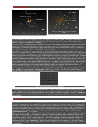
  • 2. Up to this point, we have spoken only of isolated atoms. When atoms are spaced far enough apart, as in a gas, they have very little influence upon each other, and are very much like lone atoms. But atoms within a solid have a marked effect upon each other. The forces that bind these atoms together greatly modify the behavior of the other electrons. One consequence of this close proximity of atoms is to cause the individual energy levels of an atom to break up and form bands of energy. Discrete (separate and complete) energy levels still exist within these energy bands, but there are many more energy levels than there were with the isolated atom. In some cases, energy levels will have disappeared. Figure 3 shows the difference in the energy arrangement between an isolated atom and the atom in a solid. Notice that the isolated atom (such as in gas) has energy levels, whereas the atom in a solid has energy levels grouped into Energy Bands. The upper band in the solid lines in figure 3 is called the conduction band because electrons in this band are easily removed by the application of external electric fields. Materials that have a large number of electrons in the conduction band act as good conductors of electricity. Below the conduction band is the forbidden band or energy gap. Electrons are never found in this band, but may travel back and forth through it, provided they do not come to rest in the band. The last band or valence band is composed of a series of energy levels containing valence electrons. Electrons in this band are more tightly bound to the individual atom than the electrons in the conduction band. However, the electrons in the valence band can still be moved to the conduction band with the application of energy, usually thermal energy. There are more bands below the valence band, but they are not important to the understanding of semiconductor theory and will not be discussed. The concept of energy bands is particularly important in classifying materials as conductors, semiconductors, and insulators. An electron can exist in either of two energy bands, the conduction band or the valence band. All that is necessary to move an electron from the valence band to the conduction band so it can be used for electric current, is enough energy to carry the electron through the forbidden band. The width of the forbidden band or the separation between the conduction and valence bands determines whether a substance is an insulator, semiconductor, or conductor. Figure 4 uses energy level diagrams to show the difference between insulators, semiconductors, and conductors. The energy diagram for the insulator shows the insulator with a very wide energy gap. The wider this gap, the greater the amount of energy required to move the electron from the valence band to the conduction band. Therefore, an insulator requires a large amount of energy to obtain a small amount of current. The insulator „insulates” because of the wide forbidden band or energy gap. The semiconductor, on the other hand, has a smaller forbidden band and requires less energy to move an electron from the valence band to the conduction band. Therefore, for a certain amount of applied voltage, more current will flow in the semiconductor than in the insulator. The last energy level diagram in figure 4 is that of a conductor. Notice, there is no forbidden band or energy gap and the valence and conduction bands overlap. With no energy gap, it takes a small amount of energy to move electrons into the conduction band; consequently, conductors pass electrons very easily. Covalent Bonding: The chemical activity of an atom is determined by the number of electrons in its valence shell. When the valence shell is complete, the atom is stable and shows little tendency to combine with other atoms to form solids. Only atoms that possess eight valence electrons have a complete outer shell. These atoms are referred to as inert or inactive atoms. However, if the valence shell of an atom lacks the required number of electrons to complete the shell, then the activity of the atom increases. Silicon and germanium, for example, are the most frequently used semiconductors. Both are quite similar in their structure and chemical behavior. Each has four electrons in the valence shell. Consider just germanium. Since it has fewer than the required number of eight electrons needed in the outer shell, its atoms will unite with other atoms until eight electrons are shared. This gives each atom a total of eight electrons in its valence shell; four of its own and four that it borrowed from the surrounding atoms. The sharing of valence electrons between two or more atoms produces a covalent bond between the atoms. It is this bond that holds the atoms together in an orderly structure called a crystal. A crystal is just another name for a solid whose atoms or molecules are arranged in a three-dimensional geometrical pattern commonly referred to as a lattice. Figure 1 shows a typical
  • 3. crystal structure. Each sphere in the figure represents the nucleus of an atom, and the arms that join the atoms and support the structure are the covalent bonds. As a result of this sharing process, the valence electrons are held tightly together. This can best be illustrated by the two- dimensional view of the germanium lattice in figure 2. The big circles in the figure represent the nuclei of the atoms. The small circles indicate valence electrons. Because every atom in this pattern is bonded to four other atoms, the electrons are not free to move within the crystal. As a result of this bonding, pure germanium and silicon are poor conductors of electricity. The reason they are not insulators but semiconductors is that with the proper application of heat or electrical pressure, electrons can be caused to break free of their bonds and move into the conduction band. Once in this band, they wander aimlessly through the crystal. Conduction Process As stated earlier, energy can be added to electrons by applying heat. When enough energy is absorbed by the valence electrons, it is possible for them to break some of their covalent bonds. Once the bonds are broken, the electrons move to the conduction band where they are capable of supporting electric current. When a voltage is applied to a crystal containing these conduction band electrons, the electrons move through the crystal toward the applied voltage. This movement of electrons in a semiconductor is referred to as electron current flow. There is still another type of current in a pure semiconductor. This current occurs when a covalent bond is broken and a vacancy is left in the atom by the missing valence electron. This vacancy is commonly referred to as a „hole”. The hole is considered to have a positive charge because its atom is deficient by one electron, which causes the protons to outnumber the electrons. As a result of this hole, a chain reaction begins when a nearby electron breaks its own covalent bond to fill the hole, leaving another hole. Then another electron breaks its bond to fill the previous hole, leaving still another hole. Each time an electron in this process fills a hole, it enters into a covalent bond. Even though an electron has moved from one covalent bond to another, the most important thing to remember is that the hole is also moving. Therefore, since this process of conduction resembles the movement of holes rather than electrons, it is termed hole flow (short for hole current flow or conduction by holes). Hole flow is very similar to electron flow except that the holes move toward a negative potential and in an opposite direction to that of the electron. Since hole flow results from the breaking of covalent bonds, which are at the valence band level, the electrons associated with this type of conduction contain only valence band energy and must remain in the valence band. However, the electrons associated with electron flow have conduction band energy and can, therefore, move throughout the crystal. A good analogy of hole flow is the movement of a hole through a plank with drill holes filled with balls (figure 1). When a ball is removed from the plank, a hole is left. This hole is then filled by the ball number 2, which leaves still another hole. Ball number 3 then moves into the hole left by ball number 2. This causes still another hole to appear where ball 3 was. Notice the holes are moving to the left side of the plank. This action continues until all the balls have moved one space to the right in which time the hole moved four spaces to the left and came to rest at the left-hand end of the plank. In the theory just described, two current carriers were created by the breaking of covalent bonds: the negative electron and the positive hole. These carriers are referred to as electron-hole pairs. Since the semiconductor we have been discussing contains no impurities, the number of holes in the electron-hole pairs is always equal to the number of conduction electrons. Another way of describing this condition where no impurities exist is by saying the semiconductor is intrinsic. The term intrinsic is also used to distinguish the pure semiconductor that we have been working with from one containing impurities. Doping Process The pure semiconductor mentioned earlier is basically neutral. It contains no free electrons in its conduction bands. Even with the application of thermal energy, only a few covalent bonds are broken, yielding a relatively small current flow. A much more efficient method of increasing current flow in semiconductors is by adding very small amounts of selected additives to them, generally no more than a few parts per million. These additives are called impurities and the process of adding them to crystals is referred to as doping. The purpose of semiconductor doping is to increase the number of free charges that can be moved by an external applied voltage. When an impurity increases the number of free electrons, the doped semiconductor is negative or n-type, and the impurity that is added is known as an n-typeimpurity. However, an impurity that reduces the number of free electrons, causing more holes, creates a positive or p-type semiconductor, and the impurity that was added to it is known as a p-type impurity. Semiconductors which are doped in this manner - either with n- or p-type impurities - are referred to as extrinsicsemiconductors. i) n-Type Semiconductor The n-type impurity loses its extra valence electron easily when added to a semiconductor material, and in so doing, increases the conductivity of the material by contributing a free electron. This type of impurity has 5 valence electrons and is called a pentavalent impurity. Arsenic, antimony, bismuth, and phosphorous are pentavalent impurities. Because these materials give or donate one electron to the doped material, they are also called donor impurities. When a pentavalent (donor) impurity, like arsenic, is added to germanium, it will form covalent bonds with the germanium atoms. Figure 1 illustrates this by showing an arsenic atom (As) in a germanium (Ge) lattice structure. Notice the arsenic atom in the center of the lattice. It has 5 valence electrons in its outer shell but uses only 4 of them to form covalent bonds with the germanium atoms, leaving 1 electron relatively free in the crystal structure. Pure germanium may be converted into an n-type semiconductor by „doping” it with any
  • 4. donor impurity having 5 valence electrons in its outer shell. Since this type of semiconductor (n-type) has a surplus of electrons, the electrons are considered majority carriers, while the holes, being few in number, are the minority carriers. Conduction in the n-type semiconductor, or crystal, is similar to conduction in a copper wire. That is, with voltage applied across the material, electrons will move through the crystal just as current would flow in a copper wire. The positive potential of a battery will attract the free electrons in the crystal. These electrons will leave the crystal and flow into the positive terminal of the battery. As an electron leaves the crystal, an electron from the negative terminal of the battery will enter the crystal, thus completing the current path. Therefore, the majority current carriers in the n-type material (electrons) are repelled by the negative side of the battery and move through the crystal toward the positive side of the battery. ii) p-Type Semiconductor: The second type of impurity, when added to a semiconductor material, tends to compensate for its deficiency of 1 valence electron by acquiring an electron from its neighbor. Impurities of this type have only 3 valence electrons and are called trivalent impurities. Aluminum, indium, gallium, and boron are trivalent impurities. Because these materials accept 1 electron from the doped material, they are also called acceptor impurities. A trivalent (acceptor) impurity element can also be used to dope germanium. In this case, the impurity is 1 electron short of the required amount of electrons needed to establish covalent bonds with 4 neighboring atoms. Thus, in a single covalent bond, there will be only 1 electron instead of 2. This arrangement leaves a hole in that covalent bond. Figure 2 illustrates this theory by showing what happens when germanium is doped with an indium (In) atom. Notice, the indium atom in the figure is 1 electron short of the required amount of electrons needed to form covalent bonds with 4 neighboring atoms and, therefore, creates a hole in the structure. Gallium and boron, which are also trivalent impurities, exhibit these same characteristics when added to germanium. The holes can only be present in this type semiconductor when a trivalent impurity is used. Note that a hole carrier is not created by the removal of an electron from a neutral atom, but is created when a trivalent impurity enters into covalent bonds with a tetravalent (4 valence electrons) crystal structure. The holes in this type of semiconductor (p-type) are considered the majority carriers since they are present in the material in the greatest quantity. The electrons, on the other hand, are the minority carriers. Current Flow in the p-type Material is by positive holes, instead of negative electrons. A hole moves from the positive terminal of the p-material to the negative terminal. Electrons from the external circuit enter the negative terminal of the material and fill holes in the vicinity of this terminal. At the positive terminal, electrons are removed from the covalent bonds, thus creating new holes. This process continues as the steady stream of holes (hole current) moves toward the negative terminal. Notice in both n-type and p-type materials, current flow in the external circuit consists of electrons moving out of the negative terminal of the battery and into the positive terminal of the battery. Hole flow, on the other hand, only exists within the material itself. Semiconductor Diode If we join a section of n-type semiconductor material with a similar section of p-type semiconductor material, we obtain a device known as a pn junction. (The area where the n and p regions meet is appropriately called the junction.) The usual characteristics of this device make it extremely useful in electronics as a diode rectifier. The diode is nothing more than a two-element semiconductor device that makes use of the rectifying properties of a pn junction to convert alternating current into direct current by permitting current flow in only one direction. The schematic symbol of a pn junction diode is shown in figure 1. The horizontal bar represents the cathode (n-type material) since it is the source of electrons and the arrow represents the anode (p-type material) since it is the destination of the electrons. (Notice the electron flow is against the arrow.) The label „CR1” is an alphanumerical code used to identify the diode. In this figure, we have only one diode so it is labeled CR1 (crystal rectifier number one). Junction Barrier Although the n-type material has an excess of free electrons, it is still electrically neutral. This is because the donor atoms in the n material were left with positive charges after free electrons became available by covalent bonding (the protons outnumbered the electrons). Therefore, for every free electron in the n material, there is a corresponding positively charge atom to balance it. The end result is that the p material has an overall charge of zero.
  • 5. By the same reasoning, the p-type material is also electrically neutral because the excess of holes in this material is exactly balanced by the number of electrons. Keep in mind that the holes and electrons are still free to move in the material because they are only loosely bound to their parent atoms. It would seem that if we joined the n and p materials together by one of the processes mentioned earlier, all the holes and electrons would pair up. On the contrary, this does not happen. Instead the electrons in then material diffuse (move or spread out) across the junction into the p material and fill some of the holes. At the same time, the holes in the p material diffuse across the junction into the n material and are filled byn material electrons. This process, called junction recombination, reduces the number of free electrons and holes in the vicinity of the junction. Because there is a depletion, or lack of free electrons and holes in this area, it is known as the depletion region. The loss of an electron from the n-type material created a positive ion in the n material, while the loss of a hole from the p material created a negative ion in that material. These ions are fixed in place in the crystal lattice structure and cannot move. Thus, they make up a layer of fixed charges on the two sides of the junction as shown in figure 2. On the n side of the junction, there is a layer of positively charged ions; on thep side of the junction, there is a layer of negatively charged ions. An electrostatic field is established across the junction between the oppositely charged ions. The diffusion of electrons and holes across the junction will continue until the magnitude of the electrostatic field is increased to the point where the electrons and holes no longer have enough energy to overcome it, and are repelled by the negative and positive ions respectively. At this point equilibrium is established and, for all practical purposes, the movement of carriers across the junction ceases. For this reason, the electrostatic field created by the positive and negative ions in the depletion region is called a barrier. The action just described occurs almost instantly when the junction is formed. Only the carriers in the immediate vicinity of the junction are affected. The carriers throughout the remainder of the n and p material are relatively undisturbed and remain in a balanced condition. Forward Bias An external voltage applied to a pn junction is called bias. If, for example, a battery is used to supply bias to apn junction and is connected so that its voltage opposes the junction field, it will reduce the junction barrier and, therefore, aid current flow through the junction. This type of bias is known as forward bias, and it causes the junction to offer only minimum resistance to the flow of current. The positive potential connected to the p-type material repels holes toward the junction where they neutralize some of the negative ions. At the same time the negative potential connected to the n-type material repels electrons toward the junction where they neutralize some of the positive ions. Since ions on both sides of the barrier are being neutralized, the width of the barrier decreases. Thus, the effect of the battery voltage in the forward-bias direction is to reduce the barrier potential across the junction and to allow majority carriers to cross the junction. Current flow in the forward-biased pn junction is relatively simple. An electron leaves the negative terminal of the battery and moves to the terminal of the n-type material. It enters the n material, where it is the majority carrier and moves to the edge of the junction barrier. Because of forward bias, the barrier offers less opposition to the electron and it will pass through the depletion region into the p-type material. The electron loses energy in overcoming the opposition of the junction barrier, and upon entering the p material, combines with a hole. The hole was produced when an electron was extracted from the p material by the positive potential of the battery. The created hole moves through the p material toward the junction where it combines with an electron. It is important to remember that increasing the battery voltage will increase the number of majority carriers arriving at the junction and will therefore increase the current flow. If the battery voltage is increased to the point where the barrier is greatly reduced, a heavy current will flow and the junction may be damaged from the resulting heat. Reverse Bias If the battery mentioned earlier is connected across the junction so that its voltage aids the junction, it will increase the junction barrier and thereby offer a high resistance to the current flow through the junction. This type of bias is known as reverse bias. To reverse bias a junction diode, the negative battery terminal is connected to the p- type material, and the positive battery terminal to the n-type material as shown in figure 4. The negative potential attracts the holes away from the edge of the junction barrier on the p side, while the positive potential attracts the electrons away from the edge of the barrier on the n side. This action increases the barrier width because there are more negative ions on the p side of the junction, and more positive ions on the n side of the
  • 6. junction. Notice in the figure the width of the barrier has increased. This increase in the number of ions prevents current flow across the junction by majority carriers. However, the current flow across the barrier is not quite zero because of the minority carriers crossing the junction. As you recall, when the crystal is subjected to an external source of energy (light, heat, etc.), electron-hole pairs are generated. The electron-hole pairs produce minority current carriers. There are minority current carriers in both regions: holes in the n material and electrons in the n material. With reverse bias, the electrons in the p-type material are repelled toward the junction by the negative terminal of the battery. As the electron moves across the junction, it will neutralize a positive ion in the n-type material. Similarly, the holes in the n-type material will be repelled by the positive terminal of the battery toward the junction. As the hole crosses the junction, it will neutralize a negative ion in the p-typematerial.This movement of minority carriers is called minority current flow, because the holes and electrons involved come from the electron-hole pairs that are generated in the crystal lattice structure, and not from the addition of impurity atoms. Therefore, when a pn junction is reverse biased, there will be no current flow because of majority carriers but a very small amount of current because of minority carriers crossing the junction. However, at normal operating temperatures, this small current may be neglected. In summary, the most important point to remember about the pn junction diode is its ability to offer very little resistance to current flow in the forward-bias direction but maximum resistance to current flow when reverse biased. A good way of illustrating this point is by plotting a graph of the applied voltage versus the measured current. Figure 5 shows a plot of this voltage-current relationship (characteristic curve) for a typical pn junction diode. Construction One way to produce a pn junction is to mix p-type and n-type impurities into a single crystal during the manufacturing process. By so doing, a p-region is grown over part of a semiconductor's length and n-region is grown over the other part. This is called a grown junction. Another way to produce a pn junction is to melt one type of impurity into a semiconductor of the opposite type impurity. For example, a pellet of acceptor impurity is placed on a wafer of n-type germanium and heated. Under controlled temperature conditions, the acceptor impurity fuses into the wafer to form a p-region within it. This type of junction is known as an alloy or fused-alloy junction, and is one of the most commonly used junctions. A point-contact type of diodes construction consists of a fine metal wire, that makes contact with a small area on the surface of an n-type semiconductor. The pn union is formed in this process by momentarily applying a high-surge current to the wire and the n-type semiconductor. The heat generated by this current converts the material nearest the point of contact to a p-type material. PN Junction Applications Until now, we have mentioned only one application for the diode-rectification, but there are many more applications that we have not yet discussed. Variations in doping agents, semiconductor materials, and manufacturing techniques have made it possible to produce diodes that can be used in many different applications. Examples of these types of diodes are: rectifying diodes, signal diodes, Tunnel Diodes, Zener diodes, varactors, PIN- diodes, and many more. Diode Switch In addition to their use as simple rectifiers, diodes are also used in circuits that mix signals together (mixers), detect the presence of a signal (detector), and act as a switch “to open or close a circuit”. Diodes used in these applications are commonly referred to as “signal diodes”. The simplest application of a signal diode is the basic diode switch shown in figure 1. When the input to this circuit is at zero potential, the diode is forward biased because of the zero potential on the cathode and the positive voltage on the anode. In this condition, the diode conducts and acts as a straight piece of wire because of its very low forward resistance. In effect, the input is directly coupled to the output resulting in zero volts across the output terminals. Therefore, the diode, acts as a closed switch when its anode is positive with respect to its cathode. If we apply a positive input voltage (equal to or greater than the positive voltage supplied to the anode) to the diode's cathode, the diode will be reverse biased. In this situation, the diode is cut off and acts as an open switch between the input and output terminals. Consequently, with no current flow in the circuit, the positive voltage on the diode's anode will be felt at the output terminal. Therefore, the diode acts as an open switch when it is reverse biased.
  • 7. Zener Diodes The symbol used to represent Zener diodes is illustrated in figure 1. Note that the polarity markings indicate electron flow is with the arrow symbol instead of against it as in a normal pn-junction diode. This is because breakdown diodes are operated in the reverse-bias mode, which means the current flow is by minority current carriers. Zener diodes of various sorts are used for many purposes, but their most widespread use is as voltage regulators. Once the breakdown voltage of a Zener diode is reached, the voltage across the diode remains almost constant regardless of the supply voltage. Therefore they hold the voltage across the load at a constant level. This characteristic makes Zener diodes ideal voltage regulators, and they are found in almost all solid-state circuits in this capacity. When a pn-junction diode is reverse biased, the majority carriers (holes in the p-material and electrons in the n-material) move away from the junction. The barrier or depletion region becomes wider, as illustrated in figure 2, and majority carrier current flow becomes very difficult across the high resistance of the wide depletion region. The presence of minority carriers causes a small leakage current that remains nearly constant for all reverse voltages up to a certain value. Once this value has been exceeded, there is a sudden increase in the reverse current. The voltage at which the sudden increase in current occurs is called the breakdown voltage. At breakdown, the reverse current increases very rapidly with a slight increase in the reverse voltage. Any diode can be reverse biased to the point of breakdown, but not every diode can safely dissipate the power associated with breakdown. A Zener diode is a pn junction designed to operate in the reverse-bias breakdown region. There are two distinct theories used to explain the behavior of PN junctions during breakdown: one is the Zener effect and the other is the avalanche effect. The Zener effect was first proposed by Dr. Carl Zener in 1934. According to Dr. Zener's theory, electrical breakdown in solid dielectrics occurs by a process called quantum- mechanical tunneling. The Zener effect accounts for the breakdown below 5 volts; whereas, above 5 volts the breakdown is caused by the avalanche effect. Although the avalanche effect is now accepted as an explanation of diode breakdown, the term Zener diode is used to cover both types. The true Zener effect in semiconductors can be described in terms of energy bands; however, only the two upper energy bands are of interest. The two upper bands, illustrated in figure 3, are called the conduction band and thevalence band. Figure 3 is an energy diagram of a reverse-biased Zener diode. The energy bands of the p and n materials are naturally at different levels, but reverse bias causes the valence band of the p material to overlap the energy level of the conduction band in the n material. Under this condition, the valence electrons of the p material can cross the extremely thin junction region at the overlap point without acquiring any additional energy. This action is called tunneling. When the breakdown point of thepn junction is reached, large numbers of minority carriers „tunnel” across the junction to form the current that occurs at breakdown. The tunneling phenomenon only takes place in heavily doped diodes such as Zener diodes. The second theory of reverse breakdown effect in diodes is known asavalanche breakdown and occurs at reverse voltages beyond 5 volts. This type of breakdown diode has a depletion region that is deliberately made narrower than the depletion region in the normal pn-junction diode, but thicker than that in the Zener-effect diode. The thicker depletion region is achieved by decreasing the doping level from the level used in Zener-effect diodes. The breakdown is at a higher voltage because of the higher resistivity of the material. Controlling the doping level of the material during the manufacturing process can produce breakdown voltages ranging between about 2 and 200 volts. The mechanism of avalanche breakdown is different from that of the Zener effect. In the depletion region of a pnjunction, thermal energy is responsible for the formation of electron-hole pairs. The leakage current is caused by the movement of minority electrons, which is accelerated in the electric field across the barrier region. As the reverse voltage across the depletion region is increased, the reverse voltage eventually reaches a critical value. Once the critical or breakdown voltage has been reached, sufficient energy is gained by the thermally released minority electrons to enable the electrons to rupture covalent bonds as they collide with lattice atoms. The released electrons are also accelerated by the electric field, resulting in the release of further electrons, and so on, in a chain oravalanche effect. This process is illustrated in figure 4.
  • 8. For reverse voltage slightly higher than breakdown UD, the avalanche effect releases an almost unlimited number of carriers so that the diode essentially becomes a short circuit. The current flow in this region is limited only by an external series current-limiting resistor. Operating a diode in the breakdown region does not damage it, as long as the maximum power dissipation rating of the diode is not exceeded. Removing the reverse voltage permits all carriers to return to their normal energy values and velocities. Tunnel Diode In 1958, Leo Esaki, a Japanese scientist, discovered that if a semiconductor junction diode is heavily doped with impurities, it will have a region of negative resistance. The normal junction diode uses semiconductor materials that are lightly doped with one impurity atom for ten-million semiconductor atoms. This low doping level results in a relatively wide depletion region. Conduction occurs in the normal junction diode only if the voltage applied to it is large enough to overcome the potential barrier of the junction. The schematic symbols are to indicate a tunnel diode is illustrated in figure 1. In the tunnel diode, the semiconductor materials used in forming a junction are doped to the extent of one-thousand impurity atoms for ten-million semiconductor atoms. This heavy doping produces an extremely narrow depletion zone similar to that in the Zener diode. Also because of the heavy doping, a tunnel diode exhibits an unusual current-voltage characteristic curve as compared with that of an ordinary junction diode. The characteristic curve for a tunnel diode is illustrated in figure 2 . The three most important aspects of this characteristic curve are: 1. the forward current increase to a peak (IP) with a small applied forward bias, 2. the decreasing forward current with an increasing forward bias to a minimum valley current (IV), and 3. the normal increasing forward current with further increases in the bias voltage. The portion of the characteristic curve between IP and IV is the region of negative resistance. An explanation of why a tunnel diode has a region of negative resistance is best understood by using energy levels as in the previous explanation of the Zener effect. Simply stated the theory known as quantum-mechanical tunneling is an electron crossing a pn-junction without having sufficient energy to do so otherwise. Because of the heavy doping the width of the depletion region is only one-millionth of an inch. You might think of the process simply as an arc-over between the n- and the p-side across the depletion region Figure 3 shows the equilibrium energy level diagram of a tunnel diode with no bias applied. Note that the valence band of the p-material overlaps the conduction band of the n-material. The majority electrons and holes are at the same energy level in the equilibrium state. If there is any movement of current carriers across the depletion region due to thermal energy, the net current flow will be zero because equal numbers of current carriers flow in opposite directions. Figure 4 shows the energy diagram of a tunnel diode with a small forward bias (200 millivolts) applied. The bias causes unequal energy levels between some of the majority carriers at the energy band overlap point, but not enough of a potential difference to cause the carriers to cross the forbidden gap in the normal manner. Since the valence band of the p-material and the conduction band of the n-material still overlap, current carriers tunnel across at the overlap and cause a substantial current flow. Note in figure 4 that the amount of overlap between the valence band and the conduction band decreased when forward bias was applied.
  • 9. Figure 5 is the energy diagram of a tunnel diode in which the forward bias has been increased to 400 millivolts. As you can see, the valence band and the conduction band no longer overlap at this point, and tunneling can no longer occur. The portion of the curve in figure 2 from peak point to valley point shows the decreasing current that occurs as the bias is increased, and the area of overlap becomes smaller. As the overlap between the two energy bands becomes smaller, fewer and fewer electrons can tunnel across the junction. The portion of the curve between peak point and valley point in which current decreases as the voltage increases is the negative resistance region of the tunnel diode. If the energy diagram of a tunnel diode in which the forward bias has been increased even further, then the energy bands no longer overlap and the diode operates in the same manner as a normal pn junction. The negative resistance region is the most important and most widely used characteristic of the tunnel diode. A tunnel diode biased to operate in the negative resistance region can be used as either an oscillator or an amplifier in a wide range of frequencies and applications. Very high frequency applications using the tunnel diode are possible because the tunneling action occurs so rapidly that there is no transit time effect and therefore no signal distortion. Tunnel diodes are also used extensively in high-speed switching circuits because of the speed of the tunneling action. Varactor Diode: The varactor, or varicap is a diode that exhibits the characteristics of a variable capacitor. The depletion region at the pn junction acts as the dielectric and plates of a common capacitor and is caused to expand and contract by the voltage applied to the diode. This action increases and decreases the capacitance. The schematic symbol for the varactor is shown beside. Varactors are used in tuning circuits and can be used as high-frequency amplifiers. The size of the depletion region in a varactor diode is directly related to the bias. Forward biasing makes the region smaller by repelling the current carriers toward the pn junction. If the applied voltage is large enough (about .7 volt for silicon material), the negative particles will cross the junction and join with the positive particles, as shown in figure 2. This forward biasing causes the depletion region to decrease, producing a low resistance at the pn junction and a large current flow across it. This is the condition for a forward-biased diode. On the other hand, if reverse-bias voltage is applied to the pn junction, the size of its depletion region increases as the charged particles on both sides move away from the junction. This condition, shown in figure 3, produces a high resistance between the terminals and allows little current flow (only in the microampere range). This is the operating condition for the varactor diode, which is nothing more than a special pn junction. can be applied to both the varactor and the capacitor. In this case, the size of the insulation gap of the varactor, or depletion region, is substituted for the distance between the plates of the capacitor. By varying the reverse-bias voltage applied to the varactor, the width of the „gap” may be varied. An increase in reverse bias increases the width of the gap which reduces the capacitance (C) of the pn junction. Therefore, the capacitance of the varactor is inversely proportional to the applied reverse bias.
  • 10. The ratio of varactor capacitance to reverse-bias voltage change may be as high as 10 to 1. Figure 4 shows one example of the voltage-to-capacitance ratio. The upper view shows that a reverse bias of 3 volts produces a capacitance of e.g. 20 picofarads in the varactor. If the reverse bias is increased to 6 volts, as shown in the bottom view, the depletion region widens and capacitance drops to e.g. 5 picofarads. Each 1-volt increase in bias voltage causes a 5-picofarad decrease in the capacitance of the varactor; the ratio of change is therefore 5 to 1. Of course any decrease in applied bias voltage would cause a proportionate increase in capacitance, as the depletion region narrows. Notice that the value of the capacitance is small in the picofarad range. In general, varactors are used to replace the old style variable capacitor tuning. They are used in tuning circuits of more sophisticated communication equipment and in other circuits where variable capacitance is required. One advantage of the varactor is that it allows a dc voltage to be used to tune a circuit for simple remote control or automatic tuning functions. One such application of the varactor is as a variable tuning capacitor in a receiver or transmitter tank circuit like that shown in figure 5. PIN- Diodes The pin diode consists of two narrow, but highly doped, semiconductor regions separated by a thicker, lightly-doped material called the intrinsic region. As suggested in the name, pin, one of the heavily doped regions is p-type material and the other is n- type. The same semiconductor material, usually silicon, is used for all three areas. Silicon is used most often for its power-handling capability and because it provides a highly resistive intrinsic (i) region. The pin diode acts as an ordinary diode at frequencies up to about 100 megahertz, but above this frequency the operational characteristics change. The large intrinsic region increases the transit time of electrons crossing the region. Above 100 megahertz, electrons begin to accumulate in the intrinsic region. The carrier storage in the intrinsic region causes the diode to stop acting as a rectifier and begin acting as a variable resistance. When the bias on a pin diode is varied, the microwave resistance changes from a typical value of 6 kiloohms under negative bias to about 5 ohms when the bias is positive. Thus when the diode is mounted across a transmission line or waveguide, the loading effect is insignificant while the diode is reverse biased, and the diode presents no interference to power flow. When the diode is forward biased, the resistance drops to approximately 5 ohms and most power is reflected. In other words, the diode acts as a switch when mounted in parallel with a transmission line or waveguide. Several diodes in parallel can switch power in excess of 150 kilowatts peak. The upper power limit is determined by the ability of the diode to dissipate power. The upper frequency limit is determined by the shunt capacitance of thepn junction. Pin diodes with upper limit frequencies in excess of 30 gigahertz are available. “Gunn”- Diode The discovery that microwaves could be generated by applying a steady voltage across a chip of n-type gallium-arsenide (GaAs) crystal was made in 1963 by J.B. Gunn. The Gunn oscillator is a source of microwave energy that uses the bulk-effect, gallium-arsenide semiconductor. The basic frequency of a gunn oscillator is inversely proportional to the transit time of a domain across the semiconductor. The transit time is proportional to the length of semiconductor material, and to some extent, the voltage applied. Each domain causes a pulse of current at the output; thus, the output is a frequency determined by the physical length of the semiconductor chip. In a gallium-arsenide semiconductor, empty electron conduction bands exist that are at a higher energy level than the conduction bands occupied by most of the electrons. Any electrons that do occupy the higher conduction band essentially have no mobility. If an electric field of sufficient intensity is applied to the semiconductor electrons, they will move from the low-energy conduction band to the high-energy conduction band and become essentially immobile. The immobile electrons no longer contribute to the current flow and the applied voltage progressively increases the rate at which the electrons move from the low band to the high band. As the curve in figure 1 shows, the maximum current rate is reached and begins to decrease even though the applied voltage continues to increase. The point at which the current on the curve begins to decrease is called the threshold. This point is the beginning of the negative-resistance region. Negative resistance is caused by electrons moving to the higher conduction band and becoming immobile. Gunn diodes and IMPATT diodes are similar, but not interchangeable. Gunn diodes that are made from gallium arsenide can operate at frequencies up to 200 GHz. A Gunn diode made from gallium nitride can reach 3 THz. Specifications for Gunn diodes include frequency range, minimum power, typical operating voltage, operating current, and packaging. For higher output power, a Gunn diode can be pulsed or stacked. The Gunn oscillator can deliver continuous power up to about 65 milliwatts and pulsed outputs of up to about 200 watts peak.
  • 11. Transistors The discovery of the first transistor in 1948 by a team of physicists at the Bell Telephone Laboratories sparked an interest in solid-state research that spread rapidly. The transistor, which began as a simple laboratory oddity, was rapidly developed into a semiconductor device of major importance. The transistor demonstrated for the first time in history that amplification in solids was possible. Before the transistor, amplification was achieved only with electron tubes. Transistors now perform numerous electronic tasks with new and improved transistor designs being continually put on the market. In many cases, transistors are more desirable than tubes because they are small, rugged, require no filament power, and operate at low voltages with comparatively high efficiency. The development of a family of transistors has even made possible the miniaturization of electronic circuits. Figure 1 shows a sample of the many different types of transistors you may encounter when working with electronic equipment. The first solid-state device discussed was the two-element semiconductor diode. The next device on our list is even more unique. It not only has one more element than the diode but it can amplify as well. Semiconductor devices that have-three or more elements are called transistors. The term transistor was derived from the words transfer and resistor. This term was adopted because it best describes the operation of the transistor - the transfer of an input signal current from a low-resistance circuit to a high-resistance circuit. Basically, the transistor is a solid-state device that amplifies by controlling the flow of current carriers through its semiconductor materials. Bipolar Transistors There are many different types of bipolar transistors, but their basic theory of operation is all the same. As a matter of fact, the theory we will be using to explain the operation of a transistor is the same theory used earlier with thepn-junction diode except that now two such junctions are required to form the three elements of a transistor. The three elements of the two-junction transistor are 1. the emitter, which gives off, or „emits”, current carriers (electrons or holes); 2. the base, which controls the flow of current carriers; and 3. the collector, which collects the current carriers. Classification Transistors are classified as either npn or pnp according to the arrangement of their n and p materials. Their basic construction and chemical treatment is implied by their names, „npn” or „pnp”. That is, an npn transistor is formed by introducing a thin region of p- type material between two regions of n-type material. On the other hand, a pnp transistor is formed by introducing a thin region of n-type material between two regions of p-type material. Transistors constructed in this manner have two pn junctions, as shown in figure 1. One pn junction is between the emitter and the base; the other pn junction is between the collector and the base. The two junctions share one section of semiconductor material so that the bipolar transistor actually consists of three elements.
  • 12. Since the majority and minority current carriers are different for n and p materials, it stands to reason that the internal operation of the npn and pnp transistors will also be different. The theory of operation of the npn and pnp transistors will be discussed separately in the next few paragraphs. Any additional information about the pn junction will be given as the theory of transistor operation is developed. To prepare you for the forthcoming information, the two basic types of transistors along with their circuit symbols are shown in figure 2. It should be noted that the two symbols are different. The horizontal line represents the base, the angular line with the arrow on it represents the emitter, and the other angular line represents the collector. The direction of the arrow on the emitter distinguishes the npn from the pnp transistor. If the arrow points in, (points in) the transistor is a pnp. On the other hand if the arrow points out, the transistor is an npn (not pointing in). Another point you should keep in mind is that the arrow always points in the direction of hole flow, or from the p ton sections, no matter whether the p section is the emitter or base. On the other hand, electron flow is always toward or against the arrow, just like in the junction diode. Construction he very first transistors were known as point-contact transistors. Their construction is similar to the construction of thepoint-contact diode. The difference, of course, is that the point-contact transistor has two p or n regions formed instead of one. Each of the two regions constitutes an electrode (element) of the transistor. One is named the emitter and the other is named the collector, as shown in figure 3, view A. Point-contact transistors are now practically obsolete. They have been replaced by junction transistors, which are superior to point- contact transistors in nearly all respects. The junction transistor generates less noise, handles more power, provides higher current and voltage gains, and can be mass-produced more cheaply than the point-contact transistor. Junction transistors are manufactured in much the same manner as the pn junction diode discussed earlier. However, when the pnpor npn material is grown (view B), the impurity mixing process must be reversed twice to obtain the two junctions required in a transistor. Likewise, when the alloy-junction (view C) or the diffused-junction (view D) process is used, two junctions must also be created within the crystal. Although there are numerous ways to manufacture transistors, one of the most important parts of any manufacturing process is quality control. Without good quality control, many transistors would prove unreliable because the construction and processing of a transistor govern its thermal ratings, stability, and electrical characteristics. Even though there are many variations in the transistor manufacturing processes, certain structural techniques, which yield good reliability and long life, are common to all processes: 1. Wire leads are connected to each semiconductor electrode; 2. the crystal is specially mounted to protect it against mechanical damage; and 3. the unit is sealed to prevent harmful contamination of the crystal. npn- Transistor Operation A forward-biased pn- junction is comparable to a low-resistance circuit element because it passes a high current for a given voltage. In turn, a reverse-biasedpn- junction is comparable to a high-resistance circuit element. By using the Ohm's law formula for power (P = I2 ·R) and assuming current is held constant, you can conclude that the power developed across a high resistance is greater than that developed across a low resistance. Thus, if a crystal were to contain twopn- junctions (one forward-biased and the other reverse-biased), a low-power signal could be injected into the forward-biased junction and produce a high-power signal at the reverse-biased junction. In this manner, a power gain would be obtained across the crystal. This concept, which is merely an extension of the material covered in the previous topics, is the basic theory behind how the transistor amplifies. With this information fresh in your mind, let's proceed directly to thenpn transistor.
  • 13. Just as in the case of the pn- junction diode, the n- material comprising the two end sections of the npn transistor contains a number of free electrons, while the center p section contains an excess number of holes. The action at each junction between these sections is the same as that previously described for the diode; that is, depletion regions develop and the junction barrier appears. To use the transistor as an amplifier, each of these junctions must be modified by some external bias voltage. For the transistor to function in this capacity, the first pn- junction (emitter-base junction) is biased in the forward, or low-resistance, direction. At the same time the second pn- junction (base-collector junction) is biased in the reverse, or high-resistance, direction. The letters of these elements indicate what polarity voltage to use for correct bias. For instance, notice the npn transistor shown in figure 2: The emitter, which is the first letter in the npn sequence, is connected to the negative side of the battery while the base, which is the second letter (npn), is connected to the positive side. However, since the second pn- junction is required to be reverse biased for proper transistor operation, the collector must be connected to an opposite polarity voltage (positive) than that indicated by its letter designation (npn). The voltage on the collector must also be more positive than the base, as shown beside: We now have a properly biased npn transistor. In summary, the base of the npn transistor must be positive with respect to the emitter, and the collector must be more positive than the base. npn forward-biased junction An important point to bring out at this time, which was not necessarily mentioned during the explanation of the diode, is the fact that the n- material on one side of the forward-biased junction is more heavily doped than the p material. This results in more current being carried across the junction by the majority carrier electrons from the n- material than the majority carrier holes from the p material. Therefore, conduction through the forward-biased junction, as shown in figure 3, is mainly by majority carrier electrons from the n- material (emitter). With the emitter-to-base junction in the figure biased in the forward direction, electrons leave the negative terminal of the battery and enter then- material (emitter). Since electrons are majority current carriers in the n- material, they pass easily through the emitter, cross over the junction, and combine with holes in the p material (base). For each electron that fills a hole in the p material, another electron will leave the p material (creating a new hole) and enter the positive terminal of the battery. npn Reverse Biased junction: The second pn- junction (base-to-collector), or reverse-biased junction as it is called (figure 4), blocks the majority current carriers from crossing the junction. However, there is a very small current, that does pass through this junction. This current is called minority current, or reverse current. As you recall, this current was produced by the electron-hole pairs. The minority carriers for the reverse-biased pn- junction are the electrons in the p material and the holes in the n- material. These minority carriers actually conduct the current for the reverse-biased junction when electrons from thep material enter the n material, and the holes from the n- material enter the p- material. However, the minority current electrons play the most important part in the operation of the npn transistor. npn- junction interaction The bias batteries in the figure 5 have been labeled VCC for the collector voltage supply, and VBB for the base voltage supply. Also notice the base supply battery is quite small, as indicated by the number of cells in the battery, usually 1 volt or less. However, the collector supply is generally much higher than the base supply, normally around 6 volts. This difference in supply voltages is necessary to have current flow from the emitter to the collector.
  • 14. The current flow in the external circuit is always due to the movement of free electrons. Therefore, electrons flow from the negative terminals of the supply batteries to the n-type emitter. This combined movement of electrons is known as emitter current (IE). Since electrons are the majority carriers in the n- material, they will move through the n- material emitter to the emitter-base junction. With this junction forward biased, electrons continue on into the base region. Once the electrons are in the base, which is a p-type material, they become minority carriers. Some of the electrons that move into the base recombine with available holes. For each electron that recombines, another electron moves out through the base lead as base current IB(creating a new hole for eventual combination) and returns to the base supply battery V. The electrons that recombine are lost as far as the collector is concerned. Therefore, to make the transistor more efficient, the base region is made very thin and lightly doped. This reduces the opportunity for an electron to recombine with a hole and be lost. Thus, most of the electrons that move into the base region come under the influence of the large collector reverse bias. This bias acts as forward bias for the minority carriers (electrons) in the base and, as such, accelerates them through the base-collector junction and on into the collector region. Since the collector is made of an n-type material, the electrons that reach the collector again become majority current carriers. Once in the collector, the electrons move easily through the n material and return to the positive terminal of the collector supply battery VCC as collector current (IC). To further improve on the efficiency of the transistor, the collector is made physically larger than the base for two reasons: (1) to increase the chance of collecting carriers that diffuse to the side as well as directly across the base region, and (2) to enable the collector to handle more heat without damage. In summary, total current flow in the npn transistor is through the emitter lead. Therefore, in terms of percentage, IE is 100 percent. On the other hand, since the base is very thin and lightly doped, a smaller percentage of the total current (emitter current) will flow in the base circuit than in the collector circuit. Usually no more than 2 to 5 percent of the total current is base current (IB) while the remaining 95 to 98 percent is collector current (IC). A very basic relationship exists between these two currents: IE = IB + IC In simple terms this means that the emitter current is separated into base and collector current. Since the amount of current leaving the emitter is solely a function of the emitter-base bias, and because the collector receives most of this current, a small change in emitter-base bias will have a far greater effect on the magnitude of collector current than it will have on base current. In conclusion, the relatively small emitter-base bias controls the relatively large emitter-to-collector current. pnp- Transistor Operation The pnp transistor works essentially the same as the npn transistor. However, since the emitter, base, and collector in the pnp transistor are made of materials that are different from those used in the npn transistor, different current carriers flow in the pnp unit. The majority current carriers in the pnp transistor are holes. This is in contrast to the npn transistor where the majority current carriers are electrons. To support this different type of current (hole flow), the bias batteries are reversed for the pnp transistor. A typical bias setup for the pnp transistor is shown in figure 1. Notice that the procedure used earlier to properly bias the npn transistor also applies here to thepnp transistor. The first letter (p) in the pnp sequence indicates the polarity of the voltage required for the emitter (positive), and the second letter (n) indicates the polarity of the base voltage (negative). Since the base-collector junction is always reverse biased, then the opposite polarity voltage (negative) must be used for the collector. Thus, the base of the pnp transistor must be negative with respect to the emitter, and the collector must be more negative than the base. Remember, just as in the case of the npn transistor, this difference in supply voltage is necessary to have current flow (hole flow in the case of the pnp transistor) from the emitter to the collector. Although hole flow is the predominant type of current flow in the pnp transistor, hole flow only takes place within the transistor itself, while electrons flow in the external circuit. However, it is the internal hole flow that leads to electron flow in the external wires connected to the transistor. pnp Forward-Biased Junction Now let us consider what happens when the emitter-base junction is forward biased. With the bias setup shown, the positive terminal of the battery repels the emitter holes toward the base, while the negative terminal drives the base electrons toward the emitter. When an emitter hole and a base electron meet, they combine. For each electron that combines with a hole, another electron leaves the negative terminal of the battery, and enters the base. At the same time, an electron leaves the emitter, creating a new hole, and enters the positive terminal of the battery. This movement of electrons into the base and out of the emitter constitutes base current flow (IB), and the path these electrons take is referred to as the emitter-base circuit.
  • 15. pnp Reverse-Biased Junction In the reverse-biased junction (figure 3), the negative voltage on the collector and the positive voltage on the base block the majority current carriers from crossing the junction. However, this same negative collector voltage acts as forward bias for the minority current holes in the base, which cross the junction and enter the collector. The minority current electrons in the collector also sense forward bias-the positive base voltage- and move into the base. The holes in the collector are filled by electrons that flow from the negative terminal of the battery. At the same time the electrons leave the negative terminal of the battery, other electrons in the base break their covalent bonds and enter the positive terminal of the battery. Although there is only minority current flow in the reverse-biased junction, it is still very small because of the limited number of minority current carriers. pnp Junction Interaction The interaction between the forward- and reverse-biased junctions in a pnp transistor is very similar to that in an npn transistor, except that in the pnp transistor, the majority current carriers are holes. In the pnp transistor shown in figure 4, the positive voltage on the emitter repels the holes toward the base. Once in the base, the holes combine with base electrons. But again, remember that the base region is made very thin to prevent the recombination of holes with electrons. Therefore, well over 90 percent of the holes that enter the base become attracted to the large negative collector voltage and pass right through the base. However, for each electron and hole that combine in the base region, another electron leaves the negative terminal of the base battery (V BB) and enters the base as base current (IB). At the same time an electron leaves the negative terminal of the battery, another electron leaves the emitter as IE (creating a new hole) and enters the positive terminal of VBB. Meanwhile, in the collector circuit, electrons from the collector battery (VCC) enter the collector as Ic and combine with the excess holes from the base. For each hole that is neutralized in the collector by an electron, another electron leaves the emitter and starts its way back to the positive terminal of VCC. Although current flow in the external circuit of the pnp transistor is opposite in direction to that of thenpn transistor, the majority carriers always flow from the emitter to the collector. This flow of majority carriers also results in the formation of two individual current loops within each transistor. One loop is the base-current path, and the other loop is the collector-current path. The combination of the current in both of these loops (IB + IC) results in total transistor current (IE). The most important thing to remember about the two different types of transistors is that the emitter-base voltage of thepnp transistor has the same controlling effect on collector current as that of the npn transistor. In simple terms, increasing the forward-bias voltage of a transistor reduces the emitter-base junction barrier. This action allows more carriers to reach the collector, causing an increase in current flow from the emitter to the collector and through the external circuit. Conversely, a decrease in the forward-bias voltage reduces collector current. Website: http://www.radartutorial.eu/21.semiconductors/hl19.en.html