SlideShare a Scribd company logo
1 of 8
Download to read offline
© Semiconductor Components Industries, LLC, 2013
August, 2013 − Rev. 13
1 Publication Order Number:
NTD2955/D
NTD2955, NVD2955
Power MOSFET
−60 V, −12 A, P−Channel DPAK
This Power MOSFET is designed to withstand high energy in the
avalanche and commutation modes. Designed for low−voltage, high−
speed switching applications in power supplies, converters, and power
motor controls. These devices are particularly well suited for bridge
circuits where diode speed and commutating safe operating areas are
critical and offer an additional safety margin against unexpected
voltage transients.
Features
• Avalanche Energy Specified
• IDSS and VDS(on) Specified at Elevated Temperature
• Designed for Low−Voltage, High−Speed Switching Applications and
to Withstand High Energy in the Avalanche and Commutation Modes
• NVD Prefix for Automotive and Other Applications Requiring
Unique Site and Control Change Requirements; AEC−Q101
Qualified and PPAP Capable
• These Devices are Pb−Free and are RoHS Compliant
MAXIMUM RATINGS (TJ = 25°C unless otherwise noted)
Rating Symbol Value Unit
Drain−to−Source Voltage VDSS −60 Vdc
Gate−to−Source Voltage
− Continuous
− Non−repetitive (tp ≤ 10 ms)
VGS
VGSM
± 20
± 25
Vdc
Vpk
Drain Current
Drain Current − Continuous @ Ta = 25°C
Drain Current − Single Pulse (tp ≤ 10 ms)
ID
IDM
−12
−18
Adc
Apk
Total Power Dissipation @ Ta = 25°C PD 55 W
Operating and Storage Temperature
Range
TJ, Tstg −55 to
175
°C
Single Pulse Drain−to−Source Avalanche
Energy − Starting TJ = 25°C
(VDD = 25 Vdc, VGS = 10 Vdc, Peak
IL = 12 Apk, L = 3.0 mH, RG = 25 W)
EAS 216 mJ
Thermal Resistance
− Junction−to−Case
− Junction−to−Ambient (Note 1)
− Junction−to−Ambient (Note 2)
RqJC
RqJA
RqJA
2.73
71.4
100
°C/W
Maximum Lead Temperature for Soldering
Purposes, 1/8 in. from case for
10 seconds
TL 260 °C
Stresses exceeding Maximum Ratings may damage the device. Maximum
Ratings are stress ratings only. Functional operation above the Recommended
Operating Conditions is not implied. Extended exposure to stresses above the
Recommended Operating Conditions may affect device reliability.
1. When surface mounted to an FR4 board using 1 in pad size
(Cu area = 1.127 in2).
2. When surface mounted to an FR4 board using the minimum recommended
pad size (Cu area = 0.412 in2).
D
S
G
P−Channel
http://onsemi.com
−60 V 155 mW @ −10 V, 6 A
RDS(on) TYP
−12 A
ID MAXV(BR)DSS
Y = Year
WW = Work Week
G = Pb−Free Package
1
Gate
3
Source
2
Drain
4
Drain
DPAK
CASE 369C
STYLE 2
MARKING DIAGRAMS
1 2
3
4
DPAK−3
CASE 369D
STYLE 2
1
2
3
4
YWW
NT
2955G
See detailed ordering and shipping information in the package
dimensions section on page 6 of this data sheet.
ORDERING INFORMATION
1
Gate
3
Source
2
Drain
4
Drain
YWW
NT
2955G
1
Gate
3
Source
2
Drain
4
Drain
YWW
NTP
2955G
NTD2955, NVD2955
http://onsemi.com
2
ELECTRICAL CHARACTERISTICS (TJ = 25°C unless otherwise noted)
Characteristic Symbol Min Typ Max Unit
OFF CHARACTERISTICS
Drain−to−Source Breakdown Voltage (Note 3)
(VGS = 0 Vdc, ID = −0.25 mA)
(Positive Temperature Coefficient)
V(BR)DSS
−60
−
−
67
−
−
Vdc
mV/°C
Zero Gate Voltage Drain Current
(VGS = 0 Vdc, VDS = −60 Vdc, TJ = 25°C)
(VGS = 0 Vdc, VDS = −60 Vdc, TJ = 150°C)
IDSS
−
−
−
−
−10
−100
mAdc
Gate−Body Leakage Current (VGS = ± 20 Vdc, VDS = 0 Vdc) IGSS − − −100 nAdc
ON CHARACTERISTICS (Note 3)
Gate Threshold Voltage
(VDS = VGS, ID = −250 mAdc)
(Negative Temperature Coefficient)
VGS(th)
−2.0
−
−2.8
4.5
−4.0
−
Vdc
mV/°C
Static Drain−Source On−State Resistance
(VGS = −10 Vdc, ID = −6.0 Adc)
RDS(on)
− 0.155 0.180
W
Drain−to−Source On−Voltage
(VGS = −10 Vdc, ID = −12 Adc)
(VGS = −10 Vdc, ID = −6.0 Adc, TJ = 150°C)
VDS(on)
−1.86
−
−2.6
−2.0
Vdc
Forward Transconductance (VDS = 10 Vdc, ID = 6.0 Adc) gFS 8.0 − Mhos
DYNAMIC CHARACTERISTICS
Input Capacitance
(VDS = −25 Vdc, VGS = 0 Vdc,
F = 1.0 MHz)
Ciss − 500 750 pF
Output Capacitance Coss − 150 250
Reverse Transfer Capacitance Crss − 50 100
SWITCHING CHARACTERISTICS (Notes 3 and 4)
Turn−On Delay Time
(VDD = −30 Vdc, ID = −12 A,
VGS = −10 V, RG = 9.1 W)
td(on) − 10 20 ns
Rise Time tr − 45 85
Turn−Off Delay Time td(off) − 26 40
Fall Time tf − 48 90
Gate Charge
(VDS = −48 Vdc, VGS = −10 Vdc,
ID = −12 A)
QT − 15 30 nC
QGS − 4.0 −
QGD − 7.0 −
DRAIN−SOURCE DIODE CHARACTERISTICS (Note 3)
Diode Forward On−Voltage
(IS = 12 Adc, VGS = 0 V)
(IS = 12 Adc, VGS = 0 V, TJ = 150°C)
VSD
−
−
−1.6
−1.3
−2.5
−
Vdc
Reverse Recovery Time
(IS = 12 A, dIS/dt = 100 A/ms ,VGS = 0 V)
trr − 50 ns
ta − 40 −
tb − 10 −
Reverse Recovery Stored Charge QRR − 0.10 − mC
3. Indicates Pulse Test: Pulse Width ≤ 300 ms, Duty Cycle ≤ 2%.
4. Switching characteristics are independent of operating junction temperature.
NTD2955, NVD2955
http://onsemi.com
3
TYPICAL PERFORMANCE CURVES (TJ = 25°C unless otherwise noted)
Figure 1. On−Region Characteristics Figure 2. Transfer Characteristics
Figure 3. On−Resistance versus Drain Current
and Temperature
Figure 4. On−Resistance versus Drain Current
and Gate Voltage
Figure 5. On−Resistance Variation with
Temperature
Figure 6. Drain−To−Source Leakage
Current versus Voltage
0 1 2 3 4 5
0
15
25
−VDS, DRAIN−TO−SOURCE VOLTAGE (VOLTS)
2 4 6 8 10
0
10
18
24
−VGS, GATE−TO−SOURCE VOLTAGE (VOLTS)
TJ = 25°C VDS ≥ −10 V TJ = - 55°C
25°C 125°C
VGS = -10 V -9 V
-8 V
-6 V
-5 V
-7 V
5
10
20
3 5 7 9
4
12
22
6 7 8 9 10
16
6
0 3 6 15 24
0
0.10
0.20
0.30
0 6 21 24
0.050
0.075
0.200
0.250
−ID, DRAIN CURRENT (AMPS) -ID, DRAIN CURRENT (AMPS)
TJ = 25°CVGS = −10 V
TJ = 125°C
25°C
- 55°C
12 21 3 12 15
0.05
0.15
0.25
0.100
0.225
0.125
VGS = −10 V
-15 V
189
0.35
0.40
0.175
9 18
0.150
- 50
0.6
0.8
1.2
1.6
5 20 50 60
1
100
1000
TJ, JUNCTION TEMPERATURE (°C) −VDS, DRAIN−TO−SOURCE VOLTAGE (VOLTS)
- 25 0 25 50 75 100 125 150
VGS = 0 V
VGS = −10 V
ID = −6 A
15 30 40
1.0
1.4
TJ = 125°C
175
0.4
0.2
0
1.8
2.0
100°C
-6.5 V
-5.5 V
-9.5 V
8
2
20
14
0.45
0.50
10
10 25 5535 45
−ID,DRAINCURRENT(A)
−ID,DRAINCURRENT(A)
RDS(on),DRAIN−TO−SOURCERESISTANCE(Ω)
RDS(on),DRAIN−TO−SOURCERESISTANCE(NORMALIZED)
−IDSS,LEAKAGE(nA)
NTD2955, NVD2955
http://onsemi.com
4
0.1
1
10
100
0.1 1 10 100
Figure 7. Capacitance Variation Figure 8. Gate−To−Source and Drain−To−Source
Voltage versus Total Charge
Figure 9. Resistive Switching Time
Variation versus Gate Resistance
RG, GATE RESISTANCE (W)
1 10 100
t,TIME(ns)
VDD = −30 V
ID = −12 A
VGS = −10 V
TJ = 25°C
tf
td(off)
0
QT, TOTAL GATE CHARGE (nC)
2 4 6 8
ID = 12 A
TJ = 25°C
VGS
1000
100
10
1
15
10
0
2.5
5
60
50
40
30
0
VDS
14
QT
QGS QGD
1610 12
td(on)
tr
12.5
7.5
20
0 0.25 0.75 1.75
−VSD, SOURCE−TO−DRAIN VOLTAGE (V)
VGS = 0 V
TJ = 25°C
0
10
15
5
0.5 1 1.25 1.5
10
10 0 10 15 25
GATE−TO−SOURCE OR DRAIN−TO−SOURCE VOLTAGE (V)
C,CAPACITANCE(pF)
-VGS -VDS
TJ = 25°CVDS = 0 V VGS = 0 V
1000
800
600
400
200
0
20
Ciss
Coss
Crss
5 5
Ciss
Crss
1200
Figure 10. Diode Forward Voltage versus Current
Figure 11. Maximum Rated Forward Biased
Safe Operating Area
−VDS, DRAIN−TO−SOURCE VOLTAGE (V)
VGS = −15 V
SINGLE PULSE
TC = 25°C
dc
100 ms
1 ms
10 ms
RDS(on) LIMIT
THERMAL LIMIT
PACKAGE LIMIT
Figure 12. Diode Reverse Recovery Waveform
di/dt
trr
ta
tp
IS
0.25 IS
TIME
IS
tb
ID,DRAINCURRENT(AMPS)
−VGS,GATE−TO−SOURCEVOLTAGE(V)−IS,SOURCECURRENT(AMPS)
−VDS,DRAIN−TO−SOURCEVOLTAGE(V)
NTD2955, NVD2955
http://onsemi.com
5
Figure 13. Thermal Response
t, TIME (s)
r(t),NORMALIZEDEFFECTIVE
TRANSIENTTHERMALRESISTANCE
RqJC(t) = r(t) RqJC
D CURVES APPLY FOR POWER
PULSE TRAIN SHOWN
READ TIME AT t1
TJ(pk) - TC = P(pk) RqJC(t)
P(pk)
t1
t2
DUTY CYCLE, D = t1/t2
1.0
0.1
0.01
0.2
D = 0.5
0.05
0.01
SINGLE PULSE
0.1
1.0E-05 1.0E-04 1.0E-03 1.0E-02 1.0E-01 1.0E+00 1.0E+01
0.02
NTD2955, NVD2955
http://onsemi.com
6
ORDERING INFORMATION
Device Package Shipping†
NTD2955G DPAK
(Pb−Free)
75 Units / Rail
NTD2955−1G IPAK
(Pb−Free)
75 Units / Rail
NTD2955T4G DPAK
(Pb−Free)
2500 / Tape & Reel
NVD2955T4G* DPAK
(Pb−Free)
†For information on tape and reel specifications, including part orientation and tape sizes, please refer to our Tape and Reel Packaging
Specifications Brochure, BRD8011/D.
*NVD Prefix for Automotive and Other Applications Requiring Unique Site and Control Change Requirements; AEC−Q101 Qualified and PPAP
Capable.
NTD2955, NVD2955
http://onsemi.com
7
PACKAGE DIMENSIONS
DPAK (SINGLE GAUGE)
CASE 369C
ISSUE D
STYLE 2:
PIN 1. GATE
2. DRAIN
3. SOURCE
4. DRAIN
b
D
E
b3
L3
L4
b2
e M0.005 (0.13) C
c2
A
c
C
Z
DIM MIN MAX MIN MAX
MILLIMETERSINCHES
D 0.235 0.245 5.97 6.22
E 0.250 0.265 6.35 6.73
A 0.086 0.094 2.18 2.38
b 0.025 0.035 0.63 0.89
c2 0.018 0.024 0.46 0.61
b2 0.030 0.045 0.76 1.14
c 0.018 0.024 0.46 0.61
e 0.090 BSC 2.29 BSC
b3 0.180 0.215 4.57 5.46
L4 −−− 0.040 −−− 1.01
L 0.055 0.070 1.40 1.78
L3 0.035 0.050 0.89 1.27
Z 0.155 −−− 3.93 −−−
NOTES:
1. DIMENSIONING AND TOLERANCING PER ASME
Y14.5M, 1994.
2. CONTROLLING DIMENSION: INCHES.
3. THERMAL PAD CONTOUR OPTIONAL WITHIN DI-
MENSIONS b3, L3 and Z.
4. DIMENSIONS D AND E DO NOT INCLUDE MOLD
FLASH, PROTRUSIONS, OR BURRS. MOLD
FLASH, PROTRUSIONS, OR GATE BURRS SHALL
NOT EXCEED 0.006 INCHES PER SIDE.
5. DIMENSIONS D AND E ARE DETERMINED AT THE
OUTERMOST EXTREMES OF THE PLASTIC BODY.
6. DATUMS A AND B ARE DETERMINED AT DATUM
PLANE H.1 2 3
4
5.80
0.228
2.58
0.102
1.60
0.063
6.20
0.244
3.00
0.118
6.17
0.243
ǒ mm
inches
ǓSCALE 3:1
*For additional information on our Pb−Free strategy and soldering
details, please download the ON Semiconductor Soldering and
Mounting Techniques Reference Manual, SOLDERRM/D.
SOLDERING FOOTPRINT*
H 0.370 0.410 9.40 10.41
A1 0.000 0.005 0.00 0.13
L1 0.108 REF 2.74 REF
L2 0.020 BSC 0.51 BSC
A1
HDETAIL A
SEATING
PLANE
A
B
C
L1
L
H
L2
GAUGE
PLANE
DETAIL A
ROTATED 90 CW5
NTD2955, NVD2955
http://onsemi.com
8
PACKAGE DIMENSIONS
IPAK
CASE 369D
ISSUE C
STYLE 2:
PIN 1. GATE
2. DRAIN
3. SOURCE
4. DRAIN
1 2 3
4
V
S
A
K
−T−
SEATING
PLANE
R
B
F
G
D 3 PL
M0.13 (0.005) T
C
E
J
H
DIM MIN MAX MIN MAX
MILLIMETERSINCHES
A 0.235 0.245 5.97 6.35
B 0.250 0.265 6.35 6.73
C 0.086 0.094 2.19 2.38
D 0.027 0.035 0.69 0.88
E 0.018 0.023 0.46 0.58
F 0.037 0.045 0.94 1.14
G 0.090 BSC 2.29 BSC
H 0.034 0.040 0.87 1.01
J 0.018 0.023 0.46 0.58
K 0.350 0.380 8.89 9.65
R 0.180 0.215 4.45 5.45
S 0.025 0.040 0.63 1.01
V 0.035 0.050 0.89 1.27
NOTES:
1. DIMENSIONING AND TOLERANCING PER
ANSI Y14.5M, 1982.
2. CONTROLLING DIMENSION: INCH.
Z
Z 0.155 −−− 3.93 −−−
*For additional information on our Pb−Free strategy and soldering
details, please download the ON Semiconductor Soldering and
Mounting Techniques Reference Manual, SOLDERRM/D.
SOLDERING FOOTPRINT*
5.80
0.228
2.58
0.101
1.6
0.063
6.20
0.244
3.0
0.118
6.172
0.243
ǒ mm
inches
ǓSCALE 3:1
ON Semiconductor and are registered trademarks of Semiconductor Components Industries, LLC (SCILLC). SCILLC reserves the right to make changes without further notice
to any products herein. SCILLC makes no warranty, representation or guarantee regarding the suitability of its products for any particular purpose, nor does SCILLC assume any liability
arising out of the application or use of any product or circuit, and specifically disclaims any and all liability, including without limitation special, consequential or incidental damages.
“Typical” parameters which may be provided in SCILLC data sheets and/or specifications can and do vary in different applications and actual performance may vary over time. All
operating parameters, including “Typicals” must be validated for each customer application by customer’s technical experts. SCILLC does not convey any license under its patent rights
nor the rights of others. SCILLC products are not designed, intended, or authorized for use as components in systems intended for surgical implant into the body, or other applications
intended to support or sustain life, or for any other application in which the failure of the SCILLC product could create a situation where personal injury or death may occur. Should
Buyer purchase or use SCILLC products for any such unintended or unauthorized application, Buyer shall indemnify and hold SCILLC and its officers, employees, subsidiaries, affiliates,
and distributors harmless against all claims, costs, damages, and expenses, and reasonable attorney fees arising out of, directly or indirectly, any claim of personal injury or death
associated with such unintended or unauthorized use, even if such claim alleges that SCILLC was negligent regarding the design or manufacture of the part. SCILLC is an Equal
Opportunity/Affirmative Action Employer. This literature is subject to all applicable copyright laws and is not for resale in any manner.
PUBLICATION ORDERING INFORMATION
N. American Technical Support: 800−282−9855 Toll Free
USA/Canada
Europe, Middle East and Africa Technical Support:
Phone: 421 33 790 2910
Japan Customer Focus Center
Phone: 81−3−5817−1050
NTD2955/D
LITERATURE FULFILLMENT:
Literature Distribution Center for ON Semiconductor
P.O. Box 5163, Denver, Colorado 80217 USA
Phone: 303−675−2175 or 800−344−3860 Toll Free USA/Canada
Fax: 303−675−2176 or 800−344−3867 Toll Free USA/Canada
Email: orderlit@onsemi.com
ON Semiconductor Website: www.onsemi.com
Order Literature: http://www.onsemi.com/orderlit
For additional information, please contact your local
Sales Representative

More Related Content

What's hot

Original Opto NEC2501 PS2501 2501 SOP-4 New
Original Opto NEC2501 PS2501 2501 SOP-4 NewOriginal Opto NEC2501 PS2501 2501 SOP-4 New
Original Opto NEC2501 PS2501 2501 SOP-4 Newauthelectroniccom
 
POWER TRANSFORMER STABILITY TEST
POWER TRANSFORMER STABILITY TESTPOWER TRANSFORMER STABILITY TEST
POWER TRANSFORMER STABILITY TESTRajasekaranM18
 
494197038-Baseband-6648-Commercial-Presentation.pdf
494197038-Baseband-6648-Commercial-Presentation.pdf494197038-Baseband-6648-Commercial-Presentation.pdf
494197038-Baseband-6648-Commercial-Presentation.pdfmehdiberenji
 
HA17741 General Purpose Operational Amplifier
HA17741 General Purpose Operational AmplifierHA17741 General Purpose Operational Amplifier
HA17741 General Purpose Operational AmplifierYong Heui Cho
 
Toyota 5 fbe13 forklift service repair manual
Toyota 5 fbe13 forklift service repair manualToyota 5 fbe13 forklift service repair manual
Toyota 5 fbe13 forklift service repair manualjkmsmns
 
Ampestereo250w 120510154022-phpapp01
Ampestereo250w 120510154022-phpapp01Ampestereo250w 120510154022-phpapp01
Ampestereo250w 120510154022-phpapp01adrian heriady
 
Caterpillar 3208 Diesel Engine Service Manual Copy One [PDF, ENG, 154 MB].pdf
Caterpillar 3208 Diesel Engine Service Manual Copy One [PDF, ENG, 154 MB].pdfCaterpillar 3208 Diesel Engine Service Manual Copy One [PDF, ENG, 154 MB].pdf
Caterpillar 3208 Diesel Engine Service Manual Copy One [PDF, ENG, 154 MB].pdfEguima Guima
 
Umts transmission features presentation v1[1].0
Umts transmission features presentation v1[1].0Umts transmission features presentation v1[1].0
Umts transmission features presentation v1[1].0Abi Putra Taufik
 
FlexiMultiradio Instalacion V_0.2.pdf
FlexiMultiradio Instalacion V_0.2.pdfFlexiMultiradio Instalacion V_0.2.pdf
FlexiMultiradio Instalacion V_0.2.pdfALFREDOCARRASCALGUAR2
 
Packet flow on openstack
Packet flow on openstackPacket flow on openstack
Packet flow on openstackAchhar Kalia
 
Original Opto NEC2561 PS2561 2561 DIP-4 New
Original Opto NEC2561 PS2561 2561 DIP-4 NewOriginal Opto NEC2561 PS2561 2561 DIP-4 New
Original Opto NEC2561 PS2561 2561 DIP-4 Newauthelectroniccom
 
1.2V Analog I/O library for TSMC 65nm technology
1.2V Analog I/O library for TSMC 65nm technology1.2V Analog I/O library for TSMC 65nm technology
1.2V Analog I/O library for TSMC 65nm technologySofics
 
Apostila fontes
Apostila fontesApostila fontes
Apostila fontesPessoal
 
Ultrasite technical for 4op
Ultrasite technical for 4opUltrasite technical for 4op
Ultrasite technical for 4opTempus Telcosys
 
Thesmdcodebook 130419134902-phpapp02
Thesmdcodebook 130419134902-phpapp02Thesmdcodebook 130419134902-phpapp02
Thesmdcodebook 130419134902-phpapp02Andy Jah
 

What's hot (20)

Original Opto NEC2501 PS2501 2501 SOP-4 New
Original Opto NEC2501 PS2501 2501 SOP-4 NewOriginal Opto NEC2501 PS2501 2501 SOP-4 New
Original Opto NEC2501 PS2501 2501 SOP-4 New
 
POWER TRANSFORMER STABILITY TEST
POWER TRANSFORMER STABILITY TESTPOWER TRANSFORMER STABILITY TEST
POWER TRANSFORMER STABILITY TEST
 
494197038-Baseband-6648-Commercial-Presentation.pdf
494197038-Baseband-6648-Commercial-Presentation.pdf494197038-Baseband-6648-Commercial-Presentation.pdf
494197038-Baseband-6648-Commercial-Presentation.pdf
 
Caixas+telebras+r1 r2-r3,+crt
Caixas+telebras+r1 r2-r3,+crtCaixas+telebras+r1 r2-r3,+crt
Caixas+telebras+r1 r2-r3,+crt
 
Lte training session_1
Lte training session_1Lte training session_1
Lte training session_1
 
HA17741 General Purpose Operational Amplifier
HA17741 General Purpose Operational AmplifierHA17741 General Purpose Operational Amplifier
HA17741 General Purpose Operational Amplifier
 
TDA 2003
TDA 2003TDA 2003
TDA 2003
 
Toyota 5 fbe13 forklift service repair manual
Toyota 5 fbe13 forklift service repair manualToyota 5 fbe13 forklift service repair manual
Toyota 5 fbe13 forklift service repair manual
 
Construya un amplificador estereo de 400 watts
Construya un amplificador estereo de 400 wattsConstruya un amplificador estereo de 400 watts
Construya un amplificador estereo de 400 watts
 
Ampestereo250w 120510154022-phpapp01
Ampestereo250w 120510154022-phpapp01Ampestereo250w 120510154022-phpapp01
Ampestereo250w 120510154022-phpapp01
 
Caterpillar 3208 Diesel Engine Service Manual Copy One [PDF, ENG, 154 MB].pdf
Caterpillar 3208 Diesel Engine Service Manual Copy One [PDF, ENG, 154 MB].pdfCaterpillar 3208 Diesel Engine Service Manual Copy One [PDF, ENG, 154 MB].pdf
Caterpillar 3208 Diesel Engine Service Manual Copy One [PDF, ENG, 154 MB].pdf
 
Umts transmission features presentation v1[1].0
Umts transmission features presentation v1[1].0Umts transmission features presentation v1[1].0
Umts transmission features presentation v1[1].0
 
FlexiMultiradio Instalacion V_0.2.pdf
FlexiMultiradio Instalacion V_0.2.pdfFlexiMultiradio Instalacion V_0.2.pdf
FlexiMultiradio Instalacion V_0.2.pdf
 
Packet flow on openstack
Packet flow on openstackPacket flow on openstack
Packet flow on openstack
 
Original Opto NEC2561 PS2561 2561 DIP-4 New
Original Opto NEC2561 PS2561 2561 DIP-4 NewOriginal Opto NEC2561 PS2561 2561 DIP-4 New
Original Opto NEC2561 PS2561 2561 DIP-4 New
 
1.2V Analog I/O library for TSMC 65nm technology
1.2V Analog I/O library for TSMC 65nm technology1.2V Analog I/O library for TSMC 65nm technology
1.2V Analog I/O library for TSMC 65nm technology
 
Contactor lc1 d schneider
Contactor lc1 d schneiderContactor lc1 d schneider
Contactor lc1 d schneider
 
Apostila fontes
Apostila fontesApostila fontes
Apostila fontes
 
Ultrasite technical for 4op
Ultrasite technical for 4opUltrasite technical for 4op
Ultrasite technical for 4op
 
Thesmdcodebook 130419134902-phpapp02
Thesmdcodebook 130419134902-phpapp02Thesmdcodebook 130419134902-phpapp02
Thesmdcodebook 130419134902-phpapp02
 

Similar to Original P-Channel Mosfet NTD2955T4G 2955G 2955 60V 12A TO-252 New On Semiconductor

Original N Channel Mosfet FQPF12N60 12N60 12A 600V New Fairchild
Original N Channel Mosfet FQPF12N60 12N60 12A 600V New FairchildOriginal N Channel Mosfet FQPF12N60 12N60 12A 600V New Fairchild
Original N Channel Mosfet FQPF12N60 12N60 12A 600V New FairchildAUTHELECTRONIC
 
Original N Channel Mosfet FDA59N25 59N25 59A 250V TO-3P New
Original N Channel Mosfet FDA59N25 59N25 59A 250V TO-3P NewOriginal N Channel Mosfet FDA59N25 59N25 59A 250V TO-3P New
Original N Channel Mosfet FDA59N25 59N25 59A 250V TO-3P NewAUTHELECTRONIC
 
Original Mosfet L3705N L3705 3705 55V 75A TO-220 New
Original Mosfet L3705N L3705 3705 55V 75A TO-220 NewOriginal Mosfet L3705N L3705 3705 55V 75A TO-220 New
Original Mosfet L3705N L3705 3705 55V 75A TO-220 NewAUTHELECTRONIC
 
Original N-Channel Mosfet SMK630 SMK630D 9A 200V SOT-252 New KODENSHI
Original N-Channel Mosfet SMK630 SMK630D 9A 200V SOT-252 New KODENSHIOriginal N-Channel Mosfet SMK630 SMK630D 9A 200V SOT-252 New KODENSHI
Original N-Channel Mosfet SMK630 SMK630D 9A 200V SOT-252 New KODENSHIAUTHELECTRONIC
 
Original N-CHANNEL Mosfet FQPF7N60 7N60 7A 600V TO-220F New Fairchild
Original N-CHANNEL Mosfet FQPF7N60 7N60 7A 600V TO-220F New FairchildOriginal N-CHANNEL Mosfet FQPF7N60 7N60 7A 600V TO-220F New Fairchild
Original N-CHANNEL Mosfet FQPF7N60 7N60 7A 600V TO-220F New FairchildAUTHELECTRONIC
 
FQP50N06L.pdf
FQP50N06L.pdfFQP50N06L.pdf
FQP50N06L.pdfivan ion
 
Original MOSFET N-CHANNEL IRF530NPBF IRF530N IRF530 17A 100V TO-220 New
Original MOSFET N-CHANNEL IRF530NPBF IRF530N IRF530 17A 100V TO-220 NewOriginal MOSFET N-CHANNEL IRF530NPBF IRF530N IRF530 17A 100V TO-220 New
Original MOSFET N-CHANNEL IRF530NPBF IRF530N IRF530 17A 100V TO-220 NewAUTHELECTRONIC
 
USA INDIA STOCK Original Mosfet IRF9630 RF9630 F9630 9630 200V 6.5A TO-220 New
USA INDIA STOCK Original Mosfet IRF9630 RF9630 F9630 9630 200V 6.5A TO-220 NewUSA INDIA STOCK Original Mosfet IRF9630 RF9630 F9630 9630 200V 6.5A TO-220 New
USA INDIA STOCK Original Mosfet IRF9630 RF9630 F9630 9630 200V 6.5A TO-220 NewAUTHELECTRONIC
 
Original N-Channel Mosfet FQP8N60C 8N60C 8N60 600V 7.5A TO-220F New
Original N-Channel Mosfet FQP8N60C 8N60C 8N60 600V 7.5A TO-220F NewOriginal N-Channel Mosfet FQP8N60C 8N60C 8N60 600V 7.5A TO-220F New
Original N-Channel Mosfet FQP8N60C 8N60C 8N60 600V 7.5A TO-220F NewAUTHELECTRONIC
 
Original Power MOSFET IRFP460PBF IRFP460 460 500V 20A TO-247 New Vishay Silic...
Original Power MOSFET IRFP460PBF IRFP460 460 500V 20A TO-247 New Vishay Silic...Original Power MOSFET IRFP460PBF IRFP460 460 500V 20A TO-247 New Vishay Silic...
Original Power MOSFET IRFP460PBF IRFP460 460 500V 20A TO-247 New Vishay Silic...AUTHELECTRONIC
 
Original N Channel Mosfet IRF3710PBF IRF3710 3710 37A 100V New
Original N Channel Mosfet IRF3710PBF IRF3710 3710 37A 100V NewOriginal N Channel Mosfet IRF3710PBF IRF3710 3710 37A 100V New
Original N Channel Mosfet IRF3710PBF IRF3710 3710 37A 100V NewAUTHELECTRONIC
 
Original N-Channel Mosfet MMD60R360PRH 60r360p 306 TO-252 New MagnaChips
Original N-Channel Mosfet MMD60R360PRH 60r360p 306 TO-252 New MagnaChipsOriginal N-Channel Mosfet MMD60R360PRH 60r360p 306 TO-252 New MagnaChips
Original N-Channel Mosfet MMD60R360PRH 60r360p 306 TO-252 New MagnaChipsAUTHELECTRONIC
 
Original N-Channel Mosfet FQP2N60C 2N60C 2N60 600V 2A TO-220 New Fairchild
Original N-Channel Mosfet FQP2N60C 2N60C 2N60 600V 2A TO-220 New FairchildOriginal N-Channel Mosfet FQP2N60C 2N60C 2N60 600V 2A TO-220 New Fairchild
Original N-Channel Mosfet FQP2N60C 2N60C 2N60 600V 2A TO-220 New FairchildAUTHELECTRONIC
 
Original N-Channel Mosfet FQPF2N60C 2N60C 2N60 20A 600V TO-220F New
Original N-Channel Mosfet FQPF2N60C 2N60C 2N60 20A 600V TO-220F NewOriginal N-Channel Mosfet FQPF2N60C 2N60C 2N60 20A 600V TO-220F New
Original N-Channel Mosfet FQPF2N60C 2N60C 2N60 20A 600V TO-220F NewAUTHELECTRONIC
 
Original MOSFET N-CHANNEL IRF530NPBF IRF530N IRF530 17A 100V TO-220 New
Original MOSFET N-CHANNEL IRF530NPBF IRF530N IRF530 17A 100V TO-220 NewOriginal MOSFET N-CHANNEL IRF530NPBF IRF530N IRF530 17A 100V TO-220 New
Original MOSFET N-CHANNEL IRF530NPBF IRF530N IRF530 17A 100V TO-220 NewAUTHELECTRONIC
 
Original Mosfet SM4024N SM4024NSU 4024 TO-252-3 New
Original Mosfet SM4024N SM4024NSU 4024 TO-252-3 NewOriginal Mosfet SM4024N SM4024NSU 4024 TO-252-3 New
Original Mosfet SM4024N SM4024NSU 4024 TO-252-3 NewAUTHELECTRONIC
 
Original N-Channel Mosfet 20N06 FQP20N06 60V 20A TO-220 New Fairchild
Original N-Channel Mosfet 20N06 FQP20N06 60V 20A TO-220 New FairchildOriginal N-Channel Mosfet 20N06 FQP20N06 60V 20A TO-220 New Fairchild
Original N-Channel Mosfet 20N06 FQP20N06 60V 20A TO-220 New FairchildAUTHELECTRONIC
 
Orriginal P-Channel Mosfet IRFR9024NTRPBF FR9024N 9024 55V 11A TO-252 New IR
Orriginal P-Channel Mosfet IRFR9024NTRPBF FR9024N 9024 55V 11A TO-252 New IROrriginal P-Channel Mosfet IRFR9024NTRPBF FR9024N 9024 55V 11A TO-252 New IR
Orriginal P-Channel Mosfet IRFR9024NTRPBF FR9024N 9024 55V 11A TO-252 New IRAUTHELECTRONIC
 
Original Mosfet IRF4905PBF IRF4905 IRF4905 4905 55V 74A TO-220 New Internatio...
Original Mosfet IRF4905PBF IRF4905 IRF4905 4905 55V 74A TO-220 New Internatio...Original Mosfet IRF4905PBF IRF4905 IRF4905 4905 55V 74A TO-220 New Internatio...
Original Mosfet IRF4905PBF IRF4905 IRF4905 4905 55V 74A TO-220 New Internatio...AUTHELECTRONIC
 

Similar to Original P-Channel Mosfet NTD2955T4G 2955G 2955 60V 12A TO-252 New On Semiconductor (20)

Original N Channel Mosfet FQPF12N60 12N60 12A 600V New Fairchild
Original N Channel Mosfet FQPF12N60 12N60 12A 600V New FairchildOriginal N Channel Mosfet FQPF12N60 12N60 12A 600V New Fairchild
Original N Channel Mosfet FQPF12N60 12N60 12A 600V New Fairchild
 
Original N Channel Mosfet FDA59N25 59N25 59A 250V TO-3P New
Original N Channel Mosfet FDA59N25 59N25 59A 250V TO-3P NewOriginal N Channel Mosfet FDA59N25 59N25 59A 250V TO-3P New
Original N Channel Mosfet FDA59N25 59N25 59A 250V TO-3P New
 
Original Mosfet L3705N L3705 3705 55V 75A TO-220 New
Original Mosfet L3705N L3705 3705 55V 75A TO-220 NewOriginal Mosfet L3705N L3705 3705 55V 75A TO-220 New
Original Mosfet L3705N L3705 3705 55V 75A TO-220 New
 
Original N-Channel Mosfet SMK630 SMK630D 9A 200V SOT-252 New KODENSHI
Original N-Channel Mosfet SMK630 SMK630D 9A 200V SOT-252 New KODENSHIOriginal N-Channel Mosfet SMK630 SMK630D 9A 200V SOT-252 New KODENSHI
Original N-Channel Mosfet SMK630 SMK630D 9A 200V SOT-252 New KODENSHI
 
Original N-CHANNEL Mosfet FQPF7N60 7N60 7A 600V TO-220F New Fairchild
Original N-CHANNEL Mosfet FQPF7N60 7N60 7A 600V TO-220F New FairchildOriginal N-CHANNEL Mosfet FQPF7N60 7N60 7A 600V TO-220F New Fairchild
Original N-CHANNEL Mosfet FQPF7N60 7N60 7A 600V TO-220F New Fairchild
 
FQP50N06L.pdf
FQP50N06L.pdfFQP50N06L.pdf
FQP50N06L.pdf
 
Original MOSFET N-CHANNEL IRF530NPBF IRF530N IRF530 17A 100V TO-220 New
Original MOSFET N-CHANNEL IRF530NPBF IRF530N IRF530 17A 100V TO-220 NewOriginal MOSFET N-CHANNEL IRF530NPBF IRF530N IRF530 17A 100V TO-220 New
Original MOSFET N-CHANNEL IRF530NPBF IRF530N IRF530 17A 100V TO-220 New
 
USA INDIA STOCK Original Mosfet IRF9630 RF9630 F9630 9630 200V 6.5A TO-220 New
USA INDIA STOCK Original Mosfet IRF9630 RF9630 F9630 9630 200V 6.5A TO-220 NewUSA INDIA STOCK Original Mosfet IRF9630 RF9630 F9630 9630 200V 6.5A TO-220 New
USA INDIA STOCK Original Mosfet IRF9630 RF9630 F9630 9630 200V 6.5A TO-220 New
 
Original N-Channel Mosfet FQP8N60C 8N60C 8N60 600V 7.5A TO-220F New
Original N-Channel Mosfet FQP8N60C 8N60C 8N60 600V 7.5A TO-220F NewOriginal N-Channel Mosfet FQP8N60C 8N60C 8N60 600V 7.5A TO-220F New
Original N-Channel Mosfet FQP8N60C 8N60C 8N60 600V 7.5A TO-220F New
 
Irf9530
Irf9530Irf9530
Irf9530
 
Original Power MOSFET IRFP460PBF IRFP460 460 500V 20A TO-247 New Vishay Silic...
Original Power MOSFET IRFP460PBF IRFP460 460 500V 20A TO-247 New Vishay Silic...Original Power MOSFET IRFP460PBF IRFP460 460 500V 20A TO-247 New Vishay Silic...
Original Power MOSFET IRFP460PBF IRFP460 460 500V 20A TO-247 New Vishay Silic...
 
Original N Channel Mosfet IRF3710PBF IRF3710 3710 37A 100V New
Original N Channel Mosfet IRF3710PBF IRF3710 3710 37A 100V NewOriginal N Channel Mosfet IRF3710PBF IRF3710 3710 37A 100V New
Original N Channel Mosfet IRF3710PBF IRF3710 3710 37A 100V New
 
Original N-Channel Mosfet MMD60R360PRH 60r360p 306 TO-252 New MagnaChips
Original N-Channel Mosfet MMD60R360PRH 60r360p 306 TO-252 New MagnaChipsOriginal N-Channel Mosfet MMD60R360PRH 60r360p 306 TO-252 New MagnaChips
Original N-Channel Mosfet MMD60R360PRH 60r360p 306 TO-252 New MagnaChips
 
Original N-Channel Mosfet FQP2N60C 2N60C 2N60 600V 2A TO-220 New Fairchild
Original N-Channel Mosfet FQP2N60C 2N60C 2N60 600V 2A TO-220 New FairchildOriginal N-Channel Mosfet FQP2N60C 2N60C 2N60 600V 2A TO-220 New Fairchild
Original N-Channel Mosfet FQP2N60C 2N60C 2N60 600V 2A TO-220 New Fairchild
 
Original N-Channel Mosfet FQPF2N60C 2N60C 2N60 20A 600V TO-220F New
Original N-Channel Mosfet FQPF2N60C 2N60C 2N60 20A 600V TO-220F NewOriginal N-Channel Mosfet FQPF2N60C 2N60C 2N60 20A 600V TO-220F New
Original N-Channel Mosfet FQPF2N60C 2N60C 2N60 20A 600V TO-220F New
 
Original MOSFET N-CHANNEL IRF530NPBF IRF530N IRF530 17A 100V TO-220 New
Original MOSFET N-CHANNEL IRF530NPBF IRF530N IRF530 17A 100V TO-220 NewOriginal MOSFET N-CHANNEL IRF530NPBF IRF530N IRF530 17A 100V TO-220 New
Original MOSFET N-CHANNEL IRF530NPBF IRF530N IRF530 17A 100V TO-220 New
 
Original Mosfet SM4024N SM4024NSU 4024 TO-252-3 New
Original Mosfet SM4024N SM4024NSU 4024 TO-252-3 NewOriginal Mosfet SM4024N SM4024NSU 4024 TO-252-3 New
Original Mosfet SM4024N SM4024NSU 4024 TO-252-3 New
 
Original N-Channel Mosfet 20N06 FQP20N06 60V 20A TO-220 New Fairchild
Original N-Channel Mosfet 20N06 FQP20N06 60V 20A TO-220 New FairchildOriginal N-Channel Mosfet 20N06 FQP20N06 60V 20A TO-220 New Fairchild
Original N-Channel Mosfet 20N06 FQP20N06 60V 20A TO-220 New Fairchild
 
Orriginal P-Channel Mosfet IRFR9024NTRPBF FR9024N 9024 55V 11A TO-252 New IR
Orriginal P-Channel Mosfet IRFR9024NTRPBF FR9024N 9024 55V 11A TO-252 New IROrriginal P-Channel Mosfet IRFR9024NTRPBF FR9024N 9024 55V 11A TO-252 New IR
Orriginal P-Channel Mosfet IRFR9024NTRPBF FR9024N 9024 55V 11A TO-252 New IR
 
Original Mosfet IRF4905PBF IRF4905 IRF4905 4905 55V 74A TO-220 New Internatio...
Original Mosfet IRF4905PBF IRF4905 IRF4905 4905 55V 74A TO-220 New Internatio...Original Mosfet IRF4905PBF IRF4905 IRF4905 4905 55V 74A TO-220 New Internatio...
Original Mosfet IRF4905PBF IRF4905 IRF4905 4905 55V 74A TO-220 New Internatio...
 

More from AUTHELECTRONIC

Original Power Supply IC LNK632DG LNK632 632 SOP-7 New
Original Power Supply IC LNK632DG LNK632 632 SOP-7 NewOriginal Power Supply IC LNK632DG LNK632 632 SOP-7 New
Original Power Supply IC LNK632DG LNK632 632 SOP-7 NewAUTHELECTRONIC
 
Original Relay G5RL 1A 12V New Omron 
Original Relay G5RL 1A 12V New Omron Original Relay G5RL 1A 12V New Omron 
Original Relay G5RL 1A 12V New Omron AUTHELECTRONIC
 
Original Transition-Mode PFC Controller IC LD7591GS 7591 SOP-8 New Leadtrend
Original Transition-Mode PFC Controller IC LD7591GS 7591 SOP-8 New LeadtrendOriginal Transition-Mode PFC Controller IC LD7591GS 7591 SOP-8 New Leadtrend
Original Transition-Mode PFC Controller IC LD7591GS 7591 SOP-8 New LeadtrendAUTHELECTRONIC
 
Original NPN Darlington Transistor MC1413DR2G 1413DR2G NCV1413BDG 1413BDG 141...
Original NPN Darlington Transistor MC1413DR2G 1413DR2G NCV1413BDG 1413BDG 141...Original NPN Darlington Transistor MC1413DR2G 1413DR2G NCV1413BDG 1413BDG 141...
Original NPN Darlington Transistor MC1413DR2G 1413DR2G NCV1413BDG 1413BDG 141...AUTHELECTRONIC
 
Original EEPROM IC BR93L76RFJ 93L76 RL76 SOP-8 New Rohm
Original EEPROM IC BR93L76RFJ 93L76 RL76 SOP-8 New RohmOriginal EEPROM IC BR93L76RFJ 93L76 RL76 SOP-8 New Rohm
Original EEPROM IC BR93L76RFJ 93L76 RL76 SOP-8 New RohmAUTHELECTRONIC
 
Original Advanced IGBT/Mosfet Driver TD350E 350E SOP-14 New ST Microelectronics
Original Advanced IGBT/Mosfet Driver TD350E 350E SOP-14 New ST MicroelectronicsOriginal Advanced IGBT/Mosfet Driver TD350E 350E SOP-14 New ST Microelectronics
Original Advanced IGBT/Mosfet Driver TD350E 350E SOP-14 New ST MicroelectronicsAUTHELECTRONIC
 
Original N-Channel Mosfet 2SK3562 3562 TO-220 New Toshiba
Original N-Channel Mosfet 2SK3562  3562 TO-220 New ToshibaOriginal N-Channel Mosfet 2SK3562  3562 TO-220 New Toshiba
Original N-Channel Mosfet 2SK3562 3562 TO-220 New ToshibaAUTHELECTRONIC
 
Original N-Channel Mosfet FDPF33N25 33N25 TO-220 New FairChild
Original N-Channel Mosfet FDPF33N25 33N25 TO-220 New FairChildOriginal N-Channel Mosfet FDPF33N25 33N25 TO-220 New FairChild
Original N-Channel Mosfet FDPF33N25 33N25 TO-220 New FairChildAUTHELECTRONIC
 
Original N-Channel Mosfet IRFB4020PBF 4020 TO-220-3 New International Rectifier
Original N-Channel Mosfet IRFB4020PBF 4020 TO-220-3 New International RectifierOriginal N-Channel Mosfet IRFB4020PBF 4020 TO-220-3 New International Rectifier
Original N-Channel Mosfet IRFB4020PBF 4020 TO-220-3 New International RectifierAUTHELECTRONIC
 
Original Logic IC SN74LVC14A SN54LVC14A 74LVC14A 54LVC14A SOP-14 New Texas In...
Original Logic IC SN74LVC14A SN54LVC14A 74LVC14A 54LVC14A SOP-14 New Texas In...Original Logic IC SN74LVC14A SN54LVC14A 74LVC14A 54LVC14A SOP-14 New Texas In...
Original Logic IC SN74LVC14A SN54LVC14A 74LVC14A 54LVC14A SOP-14 New Texas In...AUTHELECTRONIC
 
Original Logic IC TC74HC238AF 74HC238AF 238AF SOP-16 New Toshiba
Original Logic IC TC74HC238AF 74HC238AF 238AF SOP-16 New ToshibaOriginal Logic IC TC74HC238AF 74HC238AF 238AF SOP-16 New Toshiba
Original Logic IC TC74HC238AF 74HC238AF 238AF SOP-16 New ToshibaAUTHELECTRONIC
 
Original High Voltage Isolation IC ACS710T KLA-12CB 710T SOP-16 New
Original High Voltage Isolation IC ACS710T KLA-12CB 710T SOP-16 NewOriginal High Voltage Isolation IC ACS710T KLA-12CB 710T SOP-16 New
Original High Voltage Isolation IC ACS710T KLA-12CB 710T SOP-16 NewAUTHELECTRONIC
 
Original Voltage Regulator & Controller IC TPS54231DR 54231DR 54231 SOP-8 Ne...
Original  Voltage Regulator & Controller IC TPS54231DR 54231DR 54231 SOP-8 Ne...Original  Voltage Regulator & Controller IC TPS54231DR 54231DR 54231 SOP-8 Ne...
Original Voltage Regulator & Controller IC TPS54231DR 54231DR 54231 SOP-8 Ne...AUTHELECTRONIC
 
Original Analog Switch IC CD74HC4066PWR SN74HC4066DR 4066DR 4066PWR 4066 SOP...
Original Analog Switch IC CD74HC4066PWR  SN74HC4066DR 4066DR 4066PWR 4066 SOP...Original Analog Switch IC CD74HC4066PWR  SN74HC4066DR 4066DR 4066PWR 4066 SOP...
Original Analog Switch IC CD74HC4066PWR SN74HC4066DR 4066DR 4066PWR 4066 SOP...AUTHELECTRONIC
 
Original Microcontroller IC R5F104BDA R5F 104BDA 104 New
Original Microcontroller IC R5F104BDA R5F 104BDA 104 NewOriginal Microcontroller IC R5F104BDA R5F 104BDA 104 New
Original Microcontroller IC R5F104BDA R5F 104BDA 104 NewAUTHELECTRONIC
 
Original Power Factor Correction IC UCC28061DR 28061 SOP-16 New Texas Instrum...
Original Power Factor Correction IC UCC28061DR 28061 SOP-16 New Texas Instrum...Original Power Factor Correction IC UCC28061DR 28061 SOP-16 New Texas Instrum...
Original Power Factor Correction IC UCC28061DR 28061 SOP-16 New Texas Instrum...AUTHELECTRONIC
 
Original Led Driver IC TM1620 1620 New Shenzhen
Original Led Driver IC TM1620 1620 New ShenzhenOriginal Led Driver IC TM1620 1620 New Shenzhen
Original Led Driver IC TM1620 1620 New ShenzhenAUTHELECTRONIC
 
Original Gate Driver IC TD62083APG 62083APG 62083 DIP-18 New Toshiba
Original Gate Driver IC TD62083APG  62083APG 62083 DIP-18 New ToshibaOriginal Gate Driver IC TD62083APG  62083APG 62083 DIP-18 New Toshiba
Original Gate Driver IC TD62083APG 62083APG 62083 DIP-18 New ToshibaAUTHELECTRONIC
 
Original Zener Diode 1N5366B 5366B 5366 5W 39V New
Original Zener Diode 1N5366B 5366B 5366 5W 39V NewOriginal Zener Diode 1N5366B 5366B 5366 5W 39V New
Original Zener Diode 1N5366B 5366B 5366 5W 39V NewAUTHELECTRONIC
 
Original Audio Amplifier IC TDA7850 7850 SIP-25 New ST Microelectronics
Original Audio Amplifier IC TDA7850 7850 SIP-25 New ST MicroelectronicsOriginal Audio Amplifier IC TDA7850 7850 SIP-25 New ST Microelectronics
Original Audio Amplifier IC TDA7850 7850 SIP-25 New ST MicroelectronicsAUTHELECTRONIC
 

More from AUTHELECTRONIC (20)

Original Power Supply IC LNK632DG LNK632 632 SOP-7 New
Original Power Supply IC LNK632DG LNK632 632 SOP-7 NewOriginal Power Supply IC LNK632DG LNK632 632 SOP-7 New
Original Power Supply IC LNK632DG LNK632 632 SOP-7 New
 
Original Relay G5RL 1A 12V New Omron 
Original Relay G5RL 1A 12V New Omron Original Relay G5RL 1A 12V New Omron 
Original Relay G5RL 1A 12V New Omron 
 
Original Transition-Mode PFC Controller IC LD7591GS 7591 SOP-8 New Leadtrend
Original Transition-Mode PFC Controller IC LD7591GS 7591 SOP-8 New LeadtrendOriginal Transition-Mode PFC Controller IC LD7591GS 7591 SOP-8 New Leadtrend
Original Transition-Mode PFC Controller IC LD7591GS 7591 SOP-8 New Leadtrend
 
Original NPN Darlington Transistor MC1413DR2G 1413DR2G NCV1413BDG 1413BDG 141...
Original NPN Darlington Transistor MC1413DR2G 1413DR2G NCV1413BDG 1413BDG 141...Original NPN Darlington Transistor MC1413DR2G 1413DR2G NCV1413BDG 1413BDG 141...
Original NPN Darlington Transistor MC1413DR2G 1413DR2G NCV1413BDG 1413BDG 141...
 
Original EEPROM IC BR93L76RFJ 93L76 RL76 SOP-8 New Rohm
Original EEPROM IC BR93L76RFJ 93L76 RL76 SOP-8 New RohmOriginal EEPROM IC BR93L76RFJ 93L76 RL76 SOP-8 New Rohm
Original EEPROM IC BR93L76RFJ 93L76 RL76 SOP-8 New Rohm
 
Original Advanced IGBT/Mosfet Driver TD350E 350E SOP-14 New ST Microelectronics
Original Advanced IGBT/Mosfet Driver TD350E 350E SOP-14 New ST MicroelectronicsOriginal Advanced IGBT/Mosfet Driver TD350E 350E SOP-14 New ST Microelectronics
Original Advanced IGBT/Mosfet Driver TD350E 350E SOP-14 New ST Microelectronics
 
Original N-Channel Mosfet 2SK3562 3562 TO-220 New Toshiba
Original N-Channel Mosfet 2SK3562  3562 TO-220 New ToshibaOriginal N-Channel Mosfet 2SK3562  3562 TO-220 New Toshiba
Original N-Channel Mosfet 2SK3562 3562 TO-220 New Toshiba
 
Original N-Channel Mosfet FDPF33N25 33N25 TO-220 New FairChild
Original N-Channel Mosfet FDPF33N25 33N25 TO-220 New FairChildOriginal N-Channel Mosfet FDPF33N25 33N25 TO-220 New FairChild
Original N-Channel Mosfet FDPF33N25 33N25 TO-220 New FairChild
 
Original N-Channel Mosfet IRFB4020PBF 4020 TO-220-3 New International Rectifier
Original N-Channel Mosfet IRFB4020PBF 4020 TO-220-3 New International RectifierOriginal N-Channel Mosfet IRFB4020PBF 4020 TO-220-3 New International Rectifier
Original N-Channel Mosfet IRFB4020PBF 4020 TO-220-3 New International Rectifier
 
Original Logic IC SN74LVC14A SN54LVC14A 74LVC14A 54LVC14A SOP-14 New Texas In...
Original Logic IC SN74LVC14A SN54LVC14A 74LVC14A 54LVC14A SOP-14 New Texas In...Original Logic IC SN74LVC14A SN54LVC14A 74LVC14A 54LVC14A SOP-14 New Texas In...
Original Logic IC SN74LVC14A SN54LVC14A 74LVC14A 54LVC14A SOP-14 New Texas In...
 
Original Logic IC TC74HC238AF 74HC238AF 238AF SOP-16 New Toshiba
Original Logic IC TC74HC238AF 74HC238AF 238AF SOP-16 New ToshibaOriginal Logic IC TC74HC238AF 74HC238AF 238AF SOP-16 New Toshiba
Original Logic IC TC74HC238AF 74HC238AF 238AF SOP-16 New Toshiba
 
Original High Voltage Isolation IC ACS710T KLA-12CB 710T SOP-16 New
Original High Voltage Isolation IC ACS710T KLA-12CB 710T SOP-16 NewOriginal High Voltage Isolation IC ACS710T KLA-12CB 710T SOP-16 New
Original High Voltage Isolation IC ACS710T KLA-12CB 710T SOP-16 New
 
Original Voltage Regulator & Controller IC TPS54231DR 54231DR 54231 SOP-8 Ne...
Original  Voltage Regulator & Controller IC TPS54231DR 54231DR 54231 SOP-8 Ne...Original  Voltage Regulator & Controller IC TPS54231DR 54231DR 54231 SOP-8 Ne...
Original Voltage Regulator & Controller IC TPS54231DR 54231DR 54231 SOP-8 Ne...
 
Original Analog Switch IC CD74HC4066PWR SN74HC4066DR 4066DR 4066PWR 4066 SOP...
Original Analog Switch IC CD74HC4066PWR  SN74HC4066DR 4066DR 4066PWR 4066 SOP...Original Analog Switch IC CD74HC4066PWR  SN74HC4066DR 4066DR 4066PWR 4066 SOP...
Original Analog Switch IC CD74HC4066PWR SN74HC4066DR 4066DR 4066PWR 4066 SOP...
 
Original Microcontroller IC R5F104BDA R5F 104BDA 104 New
Original Microcontroller IC R5F104BDA R5F 104BDA 104 NewOriginal Microcontroller IC R5F104BDA R5F 104BDA 104 New
Original Microcontroller IC R5F104BDA R5F 104BDA 104 New
 
Original Power Factor Correction IC UCC28061DR 28061 SOP-16 New Texas Instrum...
Original Power Factor Correction IC UCC28061DR 28061 SOP-16 New Texas Instrum...Original Power Factor Correction IC UCC28061DR 28061 SOP-16 New Texas Instrum...
Original Power Factor Correction IC UCC28061DR 28061 SOP-16 New Texas Instrum...
 
Original Led Driver IC TM1620 1620 New Shenzhen
Original Led Driver IC TM1620 1620 New ShenzhenOriginal Led Driver IC TM1620 1620 New Shenzhen
Original Led Driver IC TM1620 1620 New Shenzhen
 
Original Gate Driver IC TD62083APG 62083APG 62083 DIP-18 New Toshiba
Original Gate Driver IC TD62083APG  62083APG 62083 DIP-18 New ToshibaOriginal Gate Driver IC TD62083APG  62083APG 62083 DIP-18 New Toshiba
Original Gate Driver IC TD62083APG 62083APG 62083 DIP-18 New Toshiba
 
Original Zener Diode 1N5366B 5366B 5366 5W 39V New
Original Zener Diode 1N5366B 5366B 5366 5W 39V NewOriginal Zener Diode 1N5366B 5366B 5366 5W 39V New
Original Zener Diode 1N5366B 5366B 5366 5W 39V New
 
Original Audio Amplifier IC TDA7850 7850 SIP-25 New ST Microelectronics
Original Audio Amplifier IC TDA7850 7850 SIP-25 New ST MicroelectronicsOriginal Audio Amplifier IC TDA7850 7850 SIP-25 New ST Microelectronics
Original Audio Amplifier IC TDA7850 7850 SIP-25 New ST Microelectronics
 

Recently uploaded

Earthing details of Electrical Substation
Earthing details of Electrical SubstationEarthing details of Electrical Substation
Earthing details of Electrical Substationstephanwindworld
 
FUNCTIONAL AND NON FUNCTIONAL REQUIREMENT
FUNCTIONAL AND NON FUNCTIONAL REQUIREMENTFUNCTIONAL AND NON FUNCTIONAL REQUIREMENT
FUNCTIONAL AND NON FUNCTIONAL REQUIREMENTSneha Padhiar
 
Energy Awareness training ppt for manufacturing process.pptx
Energy Awareness training ppt for manufacturing process.pptxEnergy Awareness training ppt for manufacturing process.pptx
Energy Awareness training ppt for manufacturing process.pptxsiddharthjain2303
 
TechTAC® CFD Report Summary: A Comparison of Two Types of Tubing Anchor Catchers
TechTAC® CFD Report Summary: A Comparison of Two Types of Tubing Anchor CatchersTechTAC® CFD Report Summary: A Comparison of Two Types of Tubing Anchor Catchers
TechTAC® CFD Report Summary: A Comparison of Two Types of Tubing Anchor Catcherssdickerson1
 
Research Methodology for Engineering pdf
Research Methodology for Engineering pdfResearch Methodology for Engineering pdf
Research Methodology for Engineering pdfCaalaaAbdulkerim
 
THE SENDAI FRAMEWORK FOR DISASTER RISK REDUCTION
THE SENDAI FRAMEWORK FOR DISASTER RISK REDUCTIONTHE SENDAI FRAMEWORK FOR DISASTER RISK REDUCTION
THE SENDAI FRAMEWORK FOR DISASTER RISK REDUCTIONjhunlian
 
Cost estimation approach: FP to COCOMO scenario based question
Cost estimation approach: FP to COCOMO scenario based questionCost estimation approach: FP to COCOMO scenario based question
Cost estimation approach: FP to COCOMO scenario based questionSneha Padhiar
 
List of Accredited Concrete Batching Plant.pdf
List of Accredited Concrete Batching Plant.pdfList of Accredited Concrete Batching Plant.pdf
List of Accredited Concrete Batching Plant.pdfisabel213075
 
DEVICE DRIVERS AND INTERRUPTS SERVICE MECHANISM.pdf
DEVICE DRIVERS AND INTERRUPTS  SERVICE MECHANISM.pdfDEVICE DRIVERS AND INTERRUPTS  SERVICE MECHANISM.pdf
DEVICE DRIVERS AND INTERRUPTS SERVICE MECHANISM.pdfAkritiPradhan2
 
Novel 3D-Printed Soft Linear and Bending Actuators
Novel 3D-Printed Soft Linear and Bending ActuatorsNovel 3D-Printed Soft Linear and Bending Actuators
Novel 3D-Printed Soft Linear and Bending ActuatorsResearcher Researcher
 
Input Output Management in Operating System
Input Output Management in Operating SystemInput Output Management in Operating System
Input Output Management in Operating SystemRashmi Bhat
 
Katarzyna Lipka-Sidor - BIM School Course
Katarzyna Lipka-Sidor - BIM School CourseKatarzyna Lipka-Sidor - BIM School Course
Katarzyna Lipka-Sidor - BIM School Coursebim.edu.pl
 
Main Memory Management in Operating System
Main Memory Management in Operating SystemMain Memory Management in Operating System
Main Memory Management in Operating SystemRashmi Bhat
 
Robotics-Asimov's Laws, Mechanical Subsystems, Robot Kinematics, Robot Dynami...
Robotics-Asimov's Laws, Mechanical Subsystems, Robot Kinematics, Robot Dynami...Robotics-Asimov's Laws, Mechanical Subsystems, Robot Kinematics, Robot Dynami...
Robotics-Asimov's Laws, Mechanical Subsystems, Robot Kinematics, Robot Dynami...Sumanth A
 
Comparative study of High-rise Building Using ETABS,SAP200 and SAFE., SAFE an...
Comparative study of High-rise Building Using ETABS,SAP200 and SAFE., SAFE an...Comparative study of High-rise Building Using ETABS,SAP200 and SAFE., SAFE an...
Comparative study of High-rise Building Using ETABS,SAP200 and SAFE., SAFE an...Erbil Polytechnic University
 
TEST CASE GENERATION GENERATION BLOCK BOX APPROACH
TEST CASE GENERATION GENERATION BLOCK BOX APPROACHTEST CASE GENERATION GENERATION BLOCK BOX APPROACH
TEST CASE GENERATION GENERATION BLOCK BOX APPROACHSneha Padhiar
 
Immutable Image-Based Operating Systems - EW2024.pdf
Immutable Image-Based Operating Systems - EW2024.pdfImmutable Image-Based Operating Systems - EW2024.pdf
Immutable Image-Based Operating Systems - EW2024.pdfDrew Moseley
 
High Voltage Engineering- OVER VOLTAGES IN ELECTRICAL POWER SYSTEMS
High Voltage Engineering- OVER VOLTAGES IN ELECTRICAL POWER SYSTEMSHigh Voltage Engineering- OVER VOLTAGES IN ELECTRICAL POWER SYSTEMS
High Voltage Engineering- OVER VOLTAGES IN ELECTRICAL POWER SYSTEMSsandhya757531
 
US Department of Education FAFSA Week of Action
US Department of Education FAFSA Week of ActionUS Department of Education FAFSA Week of Action
US Department of Education FAFSA Week of ActionMebane Rash
 

Recently uploaded (20)

Earthing details of Electrical Substation
Earthing details of Electrical SubstationEarthing details of Electrical Substation
Earthing details of Electrical Substation
 
FUNCTIONAL AND NON FUNCTIONAL REQUIREMENT
FUNCTIONAL AND NON FUNCTIONAL REQUIREMENTFUNCTIONAL AND NON FUNCTIONAL REQUIREMENT
FUNCTIONAL AND NON FUNCTIONAL REQUIREMENT
 
Energy Awareness training ppt for manufacturing process.pptx
Energy Awareness training ppt for manufacturing process.pptxEnergy Awareness training ppt for manufacturing process.pptx
Energy Awareness training ppt for manufacturing process.pptx
 
TechTAC® CFD Report Summary: A Comparison of Two Types of Tubing Anchor Catchers
TechTAC® CFD Report Summary: A Comparison of Two Types of Tubing Anchor CatchersTechTAC® CFD Report Summary: A Comparison of Two Types of Tubing Anchor Catchers
TechTAC® CFD Report Summary: A Comparison of Two Types of Tubing Anchor Catchers
 
Research Methodology for Engineering pdf
Research Methodology for Engineering pdfResearch Methodology for Engineering pdf
Research Methodology for Engineering pdf
 
Designing pile caps according to ACI 318-19.pptx
Designing pile caps according to ACI 318-19.pptxDesigning pile caps according to ACI 318-19.pptx
Designing pile caps according to ACI 318-19.pptx
 
THE SENDAI FRAMEWORK FOR DISASTER RISK REDUCTION
THE SENDAI FRAMEWORK FOR DISASTER RISK REDUCTIONTHE SENDAI FRAMEWORK FOR DISASTER RISK REDUCTION
THE SENDAI FRAMEWORK FOR DISASTER RISK REDUCTION
 
Cost estimation approach: FP to COCOMO scenario based question
Cost estimation approach: FP to COCOMO scenario based questionCost estimation approach: FP to COCOMO scenario based question
Cost estimation approach: FP to COCOMO scenario based question
 
List of Accredited Concrete Batching Plant.pdf
List of Accredited Concrete Batching Plant.pdfList of Accredited Concrete Batching Plant.pdf
List of Accredited Concrete Batching Plant.pdf
 
DEVICE DRIVERS AND INTERRUPTS SERVICE MECHANISM.pdf
DEVICE DRIVERS AND INTERRUPTS  SERVICE MECHANISM.pdfDEVICE DRIVERS AND INTERRUPTS  SERVICE MECHANISM.pdf
DEVICE DRIVERS AND INTERRUPTS SERVICE MECHANISM.pdf
 
Novel 3D-Printed Soft Linear and Bending Actuators
Novel 3D-Printed Soft Linear and Bending ActuatorsNovel 3D-Printed Soft Linear and Bending Actuators
Novel 3D-Printed Soft Linear and Bending Actuators
 
Input Output Management in Operating System
Input Output Management in Operating SystemInput Output Management in Operating System
Input Output Management in Operating System
 
Katarzyna Lipka-Sidor - BIM School Course
Katarzyna Lipka-Sidor - BIM School CourseKatarzyna Lipka-Sidor - BIM School Course
Katarzyna Lipka-Sidor - BIM School Course
 
Main Memory Management in Operating System
Main Memory Management in Operating SystemMain Memory Management in Operating System
Main Memory Management in Operating System
 
Robotics-Asimov's Laws, Mechanical Subsystems, Robot Kinematics, Robot Dynami...
Robotics-Asimov's Laws, Mechanical Subsystems, Robot Kinematics, Robot Dynami...Robotics-Asimov's Laws, Mechanical Subsystems, Robot Kinematics, Robot Dynami...
Robotics-Asimov's Laws, Mechanical Subsystems, Robot Kinematics, Robot Dynami...
 
Comparative study of High-rise Building Using ETABS,SAP200 and SAFE., SAFE an...
Comparative study of High-rise Building Using ETABS,SAP200 and SAFE., SAFE an...Comparative study of High-rise Building Using ETABS,SAP200 and SAFE., SAFE an...
Comparative study of High-rise Building Using ETABS,SAP200 and SAFE., SAFE an...
 
TEST CASE GENERATION GENERATION BLOCK BOX APPROACH
TEST CASE GENERATION GENERATION BLOCK BOX APPROACHTEST CASE GENERATION GENERATION BLOCK BOX APPROACH
TEST CASE GENERATION GENERATION BLOCK BOX APPROACH
 
Immutable Image-Based Operating Systems - EW2024.pdf
Immutable Image-Based Operating Systems - EW2024.pdfImmutable Image-Based Operating Systems - EW2024.pdf
Immutable Image-Based Operating Systems - EW2024.pdf
 
High Voltage Engineering- OVER VOLTAGES IN ELECTRICAL POWER SYSTEMS
High Voltage Engineering- OVER VOLTAGES IN ELECTRICAL POWER SYSTEMSHigh Voltage Engineering- OVER VOLTAGES IN ELECTRICAL POWER SYSTEMS
High Voltage Engineering- OVER VOLTAGES IN ELECTRICAL POWER SYSTEMS
 
US Department of Education FAFSA Week of Action
US Department of Education FAFSA Week of ActionUS Department of Education FAFSA Week of Action
US Department of Education FAFSA Week of Action
 

Original P-Channel Mosfet NTD2955T4G 2955G 2955 60V 12A TO-252 New On Semiconductor

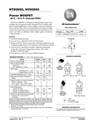
  • 1. © Semiconductor Components Industries, LLC, 2013 August, 2013 − Rev. 13 1 Publication Order Number: NTD2955/D NTD2955, NVD2955 Power MOSFET −60 V, −12 A, P−Channel DPAK This Power MOSFET is designed to withstand high energy in the avalanche and commutation modes. Designed for low−voltage, high− speed switching applications in power supplies, converters, and power motor controls. These devices are particularly well suited for bridge circuits where diode speed and commutating safe operating areas are critical and offer an additional safety margin against unexpected voltage transients. Features • Avalanche Energy Specified • IDSS and VDS(on) Specified at Elevated Temperature • Designed for Low−Voltage, High−Speed Switching Applications and to Withstand High Energy in the Avalanche and Commutation Modes • NVD Prefix for Automotive and Other Applications Requiring Unique Site and Control Change Requirements; AEC−Q101 Qualified and PPAP Capable • These Devices are Pb−Free and are RoHS Compliant MAXIMUM RATINGS (TJ = 25°C unless otherwise noted) Rating Symbol Value Unit Drain−to−Source Voltage VDSS −60 Vdc Gate−to−Source Voltage − Continuous − Non−repetitive (tp ≤ 10 ms) VGS VGSM ± 20 ± 25 Vdc Vpk Drain Current Drain Current − Continuous @ Ta = 25°C Drain Current − Single Pulse (tp ≤ 10 ms) ID IDM −12 −18 Adc Apk Total Power Dissipation @ Ta = 25°C PD 55 W Operating and Storage Temperature Range TJ, Tstg −55 to 175 °C Single Pulse Drain−to−Source Avalanche Energy − Starting TJ = 25°C (VDD = 25 Vdc, VGS = 10 Vdc, Peak IL = 12 Apk, L = 3.0 mH, RG = 25 W) EAS 216 mJ Thermal Resistance − Junction−to−Case − Junction−to−Ambient (Note 1) − Junction−to−Ambient (Note 2) RqJC RqJA RqJA 2.73 71.4 100 °C/W Maximum Lead Temperature for Soldering Purposes, 1/8 in. from case for 10 seconds TL 260 °C Stresses exceeding Maximum Ratings may damage the device. Maximum Ratings are stress ratings only. Functional operation above the Recommended Operating Conditions is not implied. Extended exposure to stresses above the Recommended Operating Conditions may affect device reliability. 1. When surface mounted to an FR4 board using 1 in pad size (Cu area = 1.127 in2). 2. When surface mounted to an FR4 board using the minimum recommended pad size (Cu area = 0.412 in2). D S G P−Channel http://onsemi.com −60 V 155 mW @ −10 V, 6 A RDS(on) TYP −12 A ID MAXV(BR)DSS Y = Year WW = Work Week G = Pb−Free Package 1 Gate 3 Source 2 Drain 4 Drain DPAK CASE 369C STYLE 2 MARKING DIAGRAMS 1 2 3 4 DPAK−3 CASE 369D STYLE 2 1 2 3 4 YWW NT 2955G See detailed ordering and shipping information in the package dimensions section on page 6 of this data sheet. ORDERING INFORMATION 1 Gate 3 Source 2 Drain 4 Drain YWW NT 2955G 1 Gate 3 Source 2 Drain 4 Drain YWW NTP 2955G
  • 2. NTD2955, NVD2955 http://onsemi.com 2 ELECTRICAL CHARACTERISTICS (TJ = 25°C unless otherwise noted) Characteristic Symbol Min Typ Max Unit OFF CHARACTERISTICS Drain−to−Source Breakdown Voltage (Note 3) (VGS = 0 Vdc, ID = −0.25 mA) (Positive Temperature Coefficient) V(BR)DSS −60 − − 67 − − Vdc mV/°C Zero Gate Voltage Drain Current (VGS = 0 Vdc, VDS = −60 Vdc, TJ = 25°C) (VGS = 0 Vdc, VDS = −60 Vdc, TJ = 150°C) IDSS − − − − −10 −100 mAdc Gate−Body Leakage Current (VGS = ± 20 Vdc, VDS = 0 Vdc) IGSS − − −100 nAdc ON CHARACTERISTICS (Note 3) Gate Threshold Voltage (VDS = VGS, ID = −250 mAdc) (Negative Temperature Coefficient) VGS(th) −2.0 − −2.8 4.5 −4.0 − Vdc mV/°C Static Drain−Source On−State Resistance (VGS = −10 Vdc, ID = −6.0 Adc) RDS(on) − 0.155 0.180 W Drain−to−Source On−Voltage (VGS = −10 Vdc, ID = −12 Adc) (VGS = −10 Vdc, ID = −6.0 Adc, TJ = 150°C) VDS(on) −1.86 − −2.6 −2.0 Vdc Forward Transconductance (VDS = 10 Vdc, ID = 6.0 Adc) gFS 8.0 − Mhos DYNAMIC CHARACTERISTICS Input Capacitance (VDS = −25 Vdc, VGS = 0 Vdc, F = 1.0 MHz) Ciss − 500 750 pF Output Capacitance Coss − 150 250 Reverse Transfer Capacitance Crss − 50 100 SWITCHING CHARACTERISTICS (Notes 3 and 4) Turn−On Delay Time (VDD = −30 Vdc, ID = −12 A, VGS = −10 V, RG = 9.1 W) td(on) − 10 20 ns Rise Time tr − 45 85 Turn−Off Delay Time td(off) − 26 40 Fall Time tf − 48 90 Gate Charge (VDS = −48 Vdc, VGS = −10 Vdc, ID = −12 A) QT − 15 30 nC QGS − 4.0 − QGD − 7.0 − DRAIN−SOURCE DIODE CHARACTERISTICS (Note 3) Diode Forward On−Voltage (IS = 12 Adc, VGS = 0 V) (IS = 12 Adc, VGS = 0 V, TJ = 150°C) VSD − − −1.6 −1.3 −2.5 − Vdc Reverse Recovery Time (IS = 12 A, dIS/dt = 100 A/ms ,VGS = 0 V) trr − 50 ns ta − 40 − tb − 10 − Reverse Recovery Stored Charge QRR − 0.10 − mC 3. Indicates Pulse Test: Pulse Width ≤ 300 ms, Duty Cycle ≤ 2%. 4. Switching characteristics are independent of operating junction temperature.
  • 3. NTD2955, NVD2955 http://onsemi.com 3 TYPICAL PERFORMANCE CURVES (TJ = 25°C unless otherwise noted) Figure 1. On−Region Characteristics Figure 2. Transfer Characteristics Figure 3. On−Resistance versus Drain Current and Temperature Figure 4. On−Resistance versus Drain Current and Gate Voltage Figure 5. On−Resistance Variation with Temperature Figure 6. Drain−To−Source Leakage Current versus Voltage 0 1 2 3 4 5 0 15 25 −VDS, DRAIN−TO−SOURCE VOLTAGE (VOLTS) 2 4 6 8 10 0 10 18 24 −VGS, GATE−TO−SOURCE VOLTAGE (VOLTS) TJ = 25°C VDS ≥ −10 V TJ = - 55°C 25°C 125°C VGS = -10 V -9 V -8 V -6 V -5 V -7 V 5 10 20 3 5 7 9 4 12 22 6 7 8 9 10 16 6 0 3 6 15 24 0 0.10 0.20 0.30 0 6 21 24 0.050 0.075 0.200 0.250 −ID, DRAIN CURRENT (AMPS) -ID, DRAIN CURRENT (AMPS) TJ = 25°CVGS = −10 V TJ = 125°C 25°C - 55°C 12 21 3 12 15 0.05 0.15 0.25 0.100 0.225 0.125 VGS = −10 V -15 V 189 0.35 0.40 0.175 9 18 0.150 - 50 0.6 0.8 1.2 1.6 5 20 50 60 1 100 1000 TJ, JUNCTION TEMPERATURE (°C) −VDS, DRAIN−TO−SOURCE VOLTAGE (VOLTS) - 25 0 25 50 75 100 125 150 VGS = 0 V VGS = −10 V ID = −6 A 15 30 40 1.0 1.4 TJ = 125°C 175 0.4 0.2 0 1.8 2.0 100°C -6.5 V -5.5 V -9.5 V 8 2 20 14 0.45 0.50 10 10 25 5535 45 −ID,DRAINCURRENT(A) −ID,DRAINCURRENT(A) RDS(on),DRAIN−TO−SOURCERESISTANCE(Ω) RDS(on),DRAIN−TO−SOURCERESISTANCE(Ω) RDS(on),DRAIN−TO−SOURCERESISTANCE(NORMALIZED) −IDSS,LEAKAGE(nA)
  • 4. NTD2955, NVD2955 http://onsemi.com 4 0.1 1 10 100 0.1 1 10 100 Figure 7. Capacitance Variation Figure 8. Gate−To−Source and Drain−To−Source Voltage versus Total Charge Figure 9. Resistive Switching Time Variation versus Gate Resistance RG, GATE RESISTANCE (W) 1 10 100 t,TIME(ns) VDD = −30 V ID = −12 A VGS = −10 V TJ = 25°C tf td(off) 0 QT, TOTAL GATE CHARGE (nC) 2 4 6 8 ID = 12 A TJ = 25°C VGS 1000 100 10 1 15 10 0 2.5 5 60 50 40 30 0 VDS 14 QT QGS QGD 1610 12 td(on) tr 12.5 7.5 20 0 0.25 0.75 1.75 −VSD, SOURCE−TO−DRAIN VOLTAGE (V) VGS = 0 V TJ = 25°C 0 10 15 5 0.5 1 1.25 1.5 10 10 0 10 15 25 GATE−TO−SOURCE OR DRAIN−TO−SOURCE VOLTAGE (V) C,CAPACITANCE(pF) -VGS -VDS TJ = 25°CVDS = 0 V VGS = 0 V 1000 800 600 400 200 0 20 Ciss Coss Crss 5 5 Ciss Crss 1200 Figure 10. Diode Forward Voltage versus Current Figure 11. Maximum Rated Forward Biased Safe Operating Area −VDS, DRAIN−TO−SOURCE VOLTAGE (V) VGS = −15 V SINGLE PULSE TC = 25°C dc 100 ms 1 ms 10 ms RDS(on) LIMIT THERMAL LIMIT PACKAGE LIMIT Figure 12. Diode Reverse Recovery Waveform di/dt trr ta tp IS 0.25 IS TIME IS tb ID,DRAINCURRENT(AMPS) −VGS,GATE−TO−SOURCEVOLTAGE(V)−IS,SOURCECURRENT(AMPS) −VDS,DRAIN−TO−SOURCEVOLTAGE(V)
  • 5. NTD2955, NVD2955 http://onsemi.com 5 Figure 13. Thermal Response t, TIME (s) r(t),NORMALIZEDEFFECTIVE TRANSIENTTHERMALRESISTANCE RqJC(t) = r(t) RqJC D CURVES APPLY FOR POWER PULSE TRAIN SHOWN READ TIME AT t1 TJ(pk) - TC = P(pk) RqJC(t) P(pk) t1 t2 DUTY CYCLE, D = t1/t2 1.0 0.1 0.01 0.2 D = 0.5 0.05 0.01 SINGLE PULSE 0.1 1.0E-05 1.0E-04 1.0E-03 1.0E-02 1.0E-01 1.0E+00 1.0E+01 0.02
  • 6. NTD2955, NVD2955 http://onsemi.com 6 ORDERING INFORMATION Device Package Shipping† NTD2955G DPAK (Pb−Free) 75 Units / Rail NTD2955−1G IPAK (Pb−Free) 75 Units / Rail NTD2955T4G DPAK (Pb−Free) 2500 / Tape & Reel NVD2955T4G* DPAK (Pb−Free) †For information on tape and reel specifications, including part orientation and tape sizes, please refer to our Tape and Reel Packaging Specifications Brochure, BRD8011/D. *NVD Prefix for Automotive and Other Applications Requiring Unique Site and Control Change Requirements; AEC−Q101 Qualified and PPAP Capable.
  • 7. NTD2955, NVD2955 http://onsemi.com 7 PACKAGE DIMENSIONS DPAK (SINGLE GAUGE) CASE 369C ISSUE D STYLE 2: PIN 1. GATE 2. DRAIN 3. SOURCE 4. DRAIN b D E b3 L3 L4 b2 e M0.005 (0.13) C c2 A c C Z DIM MIN MAX MIN MAX MILLIMETERSINCHES D 0.235 0.245 5.97 6.22 E 0.250 0.265 6.35 6.73 A 0.086 0.094 2.18 2.38 b 0.025 0.035 0.63 0.89 c2 0.018 0.024 0.46 0.61 b2 0.030 0.045 0.76 1.14 c 0.018 0.024 0.46 0.61 e 0.090 BSC 2.29 BSC b3 0.180 0.215 4.57 5.46 L4 −−− 0.040 −−− 1.01 L 0.055 0.070 1.40 1.78 L3 0.035 0.050 0.89 1.27 Z 0.155 −−− 3.93 −−− NOTES: 1. DIMENSIONING AND TOLERANCING PER ASME Y14.5M, 1994. 2. CONTROLLING DIMENSION: INCHES. 3. THERMAL PAD CONTOUR OPTIONAL WITHIN DI- MENSIONS b3, L3 and Z. 4. DIMENSIONS D AND E DO NOT INCLUDE MOLD FLASH, PROTRUSIONS, OR BURRS. MOLD FLASH, PROTRUSIONS, OR GATE BURRS SHALL NOT EXCEED 0.006 INCHES PER SIDE. 5. DIMENSIONS D AND E ARE DETERMINED AT THE OUTERMOST EXTREMES OF THE PLASTIC BODY. 6. DATUMS A AND B ARE DETERMINED AT DATUM PLANE H.1 2 3 4 5.80 0.228 2.58 0.102 1.60 0.063 6.20 0.244 3.00 0.118 6.17 0.243 ǒ mm inches ǓSCALE 3:1 *For additional information on our Pb−Free strategy and soldering details, please download the ON Semiconductor Soldering and Mounting Techniques Reference Manual, SOLDERRM/D. SOLDERING FOOTPRINT* H 0.370 0.410 9.40 10.41 A1 0.000 0.005 0.00 0.13 L1 0.108 REF 2.74 REF L2 0.020 BSC 0.51 BSC A1 HDETAIL A SEATING PLANE A B C L1 L H L2 GAUGE PLANE DETAIL A ROTATED 90 CW5
  • 8. NTD2955, NVD2955 http://onsemi.com 8 PACKAGE DIMENSIONS IPAK CASE 369D ISSUE C STYLE 2: PIN 1. GATE 2. DRAIN 3. SOURCE 4. DRAIN 1 2 3 4 V S A K −T− SEATING PLANE R B F G D 3 PL M0.13 (0.005) T C E J H DIM MIN MAX MIN MAX MILLIMETERSINCHES A 0.235 0.245 5.97 6.35 B 0.250 0.265 6.35 6.73 C 0.086 0.094 2.19 2.38 D 0.027 0.035 0.69 0.88 E 0.018 0.023 0.46 0.58 F 0.037 0.045 0.94 1.14 G 0.090 BSC 2.29 BSC H 0.034 0.040 0.87 1.01 J 0.018 0.023 0.46 0.58 K 0.350 0.380 8.89 9.65 R 0.180 0.215 4.45 5.45 S 0.025 0.040 0.63 1.01 V 0.035 0.050 0.89 1.27 NOTES: 1. DIMENSIONING AND TOLERANCING PER ANSI Y14.5M, 1982. 2. CONTROLLING DIMENSION: INCH. Z Z 0.155 −−− 3.93 −−− *For additional information on our Pb−Free strategy and soldering details, please download the ON Semiconductor Soldering and Mounting Techniques Reference Manual, SOLDERRM/D. SOLDERING FOOTPRINT* 5.80 0.228 2.58 0.101 1.6 0.063 6.20 0.244 3.0 0.118 6.172 0.243 ǒ mm inches ǓSCALE 3:1 ON Semiconductor and are registered trademarks of Semiconductor Components Industries, LLC (SCILLC). SCILLC reserves the right to make changes without further notice to any products herein. SCILLC makes no warranty, representation or guarantee regarding the suitability of its products for any particular purpose, nor does SCILLC assume any liability arising out of the application or use of any product or circuit, and specifically disclaims any and all liability, including without limitation special, consequential or incidental damages. “Typical” parameters which may be provided in SCILLC data sheets and/or specifications can and do vary in different applications and actual performance may vary over time. All operating parameters, including “Typicals” must be validated for each customer application by customer’s technical experts. SCILLC does not convey any license under its patent rights nor the rights of others. SCILLC products are not designed, intended, or authorized for use as components in systems intended for surgical implant into the body, or other applications intended to support or sustain life, or for any other application in which the failure of the SCILLC product could create a situation where personal injury or death may occur. Should Buyer purchase or use SCILLC products for any such unintended or unauthorized application, Buyer shall indemnify and hold SCILLC and its officers, employees, subsidiaries, affiliates, and distributors harmless against all claims, costs, damages, and expenses, and reasonable attorney fees arising out of, directly or indirectly, any claim of personal injury or death associated with such unintended or unauthorized use, even if such claim alleges that SCILLC was negligent regarding the design or manufacture of the part. SCILLC is an Equal Opportunity/Affirmative Action Employer. This literature is subject to all applicable copyright laws and is not for resale in any manner. PUBLICATION ORDERING INFORMATION N. American Technical Support: 800−282−9855 Toll Free USA/Canada Europe, Middle East and Africa Technical Support: Phone: 421 33 790 2910 Japan Customer Focus Center Phone: 81−3−5817−1050 NTD2955/D LITERATURE FULFILLMENT: Literature Distribution Center for ON Semiconductor P.O. Box 5163, Denver, Colorado 80217 USA Phone: 303−675−2175 or 800−344−3860 Toll Free USA/Canada Fax: 303−675−2176 or 800−344−3867 Toll Free USA/Canada Email: orderlit@onsemi.com ON Semiconductor Website: www.onsemi.com Order Literature: http://www.onsemi.com/orderlit For additional information, please contact your local Sales Representative