SlideShare a Scribd company logo
1 of 11
Download to read offline
APPLICATION NOTE
Thyristors & Triacs - Ten Golden Rules for
Success In Your Application.
This Technical Publication aims to provide an
interesting, descriptive and practical introduction to the
golden rules that should be followed in the successful
use of thyristors and triacs in power control applications.
Thyristor
A thyristor is a controlled rectifier where the
unidirectional current flow from anode to cathode is
initiated by a small signal current from gate to cathode.
Fig. 1. Thyristor.
The thyristor’s operating characteristic is shown in
Fig. 2.
Fig. 2. Thyristor V/I characteristic.
Turn-on
A thyristor is turned on by making its gate positive with
respect to its cathode, thereby causing current flow into
the gate. When the gate voltage reaches the threshold
voltage VGT and the resulting current reaches the
threshold current IGT, within a very short time known as
the gate-controlled turn-on time, tgt, the load current can
flow from ’a’ to ’k’. If the gate current consists of a very
narrow pulse, say less than 1µs, its peak level will have
to increase for progressively narrower pulse widths to
guarantee triggering.
When the load current reaches the thyristor’s latching
current IL, load current flow will be maintained even after
removal of the gate current. As long as adequate load
current continues to flow, the thyristor will continue to
conduct without the gate current. It is said to be latched
ON.
Note that the VGT, IGT and IL specifications given in data
are at 25 ˚C. These parameters will increase at lower
temperatures,sothedrivecircuitmust provide adequate
voltage and current amplitude and duration for the
lowest expected operating temperature.
Rule 1. To turn a thyristor (or triac) ON, a gate current
≥ IGT must be applied until the load current is
≥ IL. This condition must be met at the lowest
expected operating temperature.
Sensitive gate thyristors such as the BT150 can be
prone to turn-on by anode to cathode leakage current
at high temperatures. If the junction temperature Tj is
increased above Tj max, a point will be reached where
the leakage current will be high enough to trigger the
thyristor’s sensitive gate. It will then have lost its ability
to remain in the blocking state and conduction will
commence without the application of an external gate
current.
This methodofspurious turn-oncan beavoided byusing
one or more of the following solutions:
1. Ensure that the temperature does not exceed Tj max.
2. Use a thyristor with a less sensitive gate such as the
BT151, or reduce the existing thyristor’s sensitivity by
including a gate-to-cathode resistor of 1kΩ or less.
a k
g
On-state
characteristic
Off-state
characteristic
Avalanche
breakdown
region
Reverse
characteristic
Reverse
current
Forward
current
Reverse
voltage
Forward
voltage
I
L
I
H
3. If it is not possible to use a less sensitive thyristor due
to circuit requirements, apply a small degree of reverse
biasing to the gate during the ’off’ periods. This has the
effect of increasing IL. During negative gate current flow,
particularattention shouldbe paidto minimisingthegate
power dissipation.
Turn-off (commutation)
In order to turn the thyristor off, the load current must
be reduced below its holding current IH for sufficient time
to allow all the mobile charge carriers to vacate the
junction. This is achieved by "forced commutation" in
DC circuits or at the end of the conducting half cycle in
AC circuits. (Forced commutation is when the load
circuit causes the load current to reduce to zero to allow
the thyristor to turn off.) At this point, the thyristor will
have returned to its fully blocking state.
If the load current is not maintained below IH for long
enough, the thyristor will not have returned to the fully
blocking state by the time the anode-to-cathode voltage
rises again. It might then return to the conducting state
without an externally-applied gate current.
Note that IH is also specified at room temperature and,
likeIL,itreduces athighertemperatures.Thecircuitmust
therefore allow sufficient time for the load current to fall
below IH at the maximum expected operating
temperature for successful commutation.
Rule 2. To turn off (commutate) a thyristor (or triac),
the load current must be < IH for sufficient time
to allow a return to the blocking state. This
condition must be met at the highest expected
operating temperature.
Triac
A triac can be regarded as a "bidirectional thyristor"
because it conducts in both directions. For standard
triacs, current flow in either direction between the main
terminals MT1 and MT2 is initiated by a small signal
current applied between MT1 and the gate terminal.
Fig. 3. Triac.
Turn-on
Unlike thyristors, standard triacs can be triggered by
positive or negative current flow between the gate and
MT1. (The rules for VGT, IGT and IL are the same as for
thyristors. See Rule 1.) This permits triggering in four
"quadrants" as summarised in Fig. 4.
Fig. 4. Triac triggering quadrants.
Fig. 5. Triac V/I characteristic.
Where the gate is to be triggered by DC or unipolar
pulses at zero-crossing of the load current, negative
gate current is to be preferred for the following reasons.
Theinternal construction of the triac means that the gate
is more remote from the main current-carrying region
when operating in the 3+
quadrant. This results in:
1. Higher IGT -> higher peak IG required,
2. Longer delay between IG and the commencement of
load current flow -> longer duration of IG required,
3. Much lower dIT/dt capability -> progressive gate
degradation can occur when controlling loads with high
initial dI/dt (e.g. cold incandescent lamp filaments),
4. Higher IL (also true for 1-
operation) -> longer IG
duration might be needed for very small loads when
conducting from the beginning of a mains half cycle to
allow the load current to reach the higher IL.
V MT2
V G
11
3 3
+-
- +
MT1
MT2+
G+
MT2+
G+
MT2- MT2-
G-
G-
MT1
MT1 MT1
On-state
Off-state
Reverse
current
Forward
current
Reverse
voltage
Forward
voltage
I
L
I
H
L
I
H
I
T2-
T2+
QUADRANT
1
QUADRANT
3
QUADRANT
2
QUADRANT
4
MT2 MT1
g
In standard AC phase control circuits such as lamp
dimmers and domestic motor speed controls, the gate
and MT2 polarities are always the same. This means
that operation is always in the 1+
and 3-
quadrants where
the triac’s switching parameters are the same. This
results in symmetrical triac switching where the gate is
at its most sensitive.
Note:- The 1+
, 1-
, 3-
and 3+
notation for the four triggering
quadrants is used for brevity instead of writing "MT2+,
G+" for 1+
, etc. It is derived from the graph of the triac’s
V/I characteristic. Positive MT2 corresponds with
positive current flow into MT2, and vice versa (see
Fig. 5). Hence, operation is in quadrants 1 and 3 only.
The + and - superscripts refer to inward and outward
gate current respectively.
Rule 3. When designing a triac triggering circuit, avoid
triggering in the 3+
quadrant (MT2-, G+) where
possible.
Alternative turn-on methods
There are undesirable ways a triac can be turned on.
Some are benign, while some are potentially
destructive.
(a) Noisy gate signal
In electrically noisy environments, spurious triggering
can occur if the noise voltage on the gate exceeds VGT
and enough gate current flows to initiate regenerative
action within the triac. The first line of defence is to
minimise the occurrence of the noise in the first place.
This is best achieved by keeping the gate connections
as short as possible and ensuring that the common
return from the gate drive circuit connects directly to the
MT1 pin (or cathode in the case of a thyristor). In
situations where the gate connections are hard wired,
twisted pair wires or even shielded cable might be
necessary to minimise pickup.
Additional noise immunity can be provided by adding a
resistor of 1kΩ or less between the gate and MT1 to
reduce the gate sensitivity. If a high frequency bypass
capacitor is also used, it is advisable to include a series
resistor between it and the gate to minimise peak
capacitor currents through the gate and minimise the
possibilityofovercurrent damagetothetriac’sgate area.
Alternatively, use a series H triac (e.g. BT139-600H).
These are insensitive types with 10mA min IGT specs
which are specifically designed to provide a high
degree of noise immunity.
Rule 4. To minimise noise pickup, keep gate
connection length to a minimum. Take the
return directly to MT1 (or cathode). If hard
wired, use twisted pair or shielded cable. Fit a
resistor of 1kΩ or less between gate and MT1.
Fit a bypass capacitor in conjunction with a
series resistor to the gate.
Alternatively, use an insensitive series H triac.
(b) Exceeding the max rate of change of
commutating voltage dVCOM/dt
This is most likely to occur when driving a highly reactive
load where there is substantial phase shift between the
load voltage and current waveforms. When the triac
commutates as the load current passes through zero,
the voltage will not be zero because of the phase shift
(see Fig. 6). The triac is then suddenly required to block
this voltage. The resulting rate of change of
commutating voltage can force the triac back into
conduction if it exceeds the permitted dVCOM/dt. This is
because the mobile charge carriers have not been given
time to clear the junction.
The dVCOM/dt capability is affected by two conditions:-
1. The rate of fall of load current at commutation,
dICOM/dt. Higher dICOM/dt lowers the dVCOM/dt capability.
2. The junction temperature Tj. Higher Tj lowers the
dVCOM/dt capability.
If the triac’s dVCOM/dt is likely to be exceeded, false
triggering can be avoided by use of an RC snubber
across MT1-MT2 to limit the rate of change of voltage.
Common values are 100Ω carbon composition resistor,
chosen for its surge current handling, and 100nF.
Alternatively, use a Hi-Com triac.
Note that the resistor should never be omitted from the
snubber because therewould thenbe nothing to prevent
the capacitor from dumping its charge into the triac and
creating damaging dIT/dt during unfavourable turn-on
conditions.
Fig. 6. Triac dICOM/dt and dVCOM/dt.
TimeOn-state
voltage
I V
Reverse
recovery
current
Re-applied
Conducting
current
voltage
dIcom/dt
dVcom/dt
(c) Exceeding the max rate of change of
commutating current dICOM/dt
Higher dICOM/dt is caused by higher load current, higher
mains frequency (assuming sinewave current) or non
sinewave load current. A well known cause of non
sinewave load current and high dICOM/dt is rectifier-fed
inductive loads. These can often result in commutation
failurein standardtriacsas thesupplyvoltagefalls below
the back EMF of the load and the triac current collapses
suddenly to zero. The effect of this is illustrated in Fig. 7.
During this condition of zero triac current, the load
current will be "freewheeling" around the bridge rectifier
circuit. Loads of this nature can generate such high
dICOM/dt that the triac cannot support even the gentle
reapplied dV/dt of a 50Hz waveform rising from zero
volts. There will then be no benefit in adding a snubber
across the triac because dVCOM/dt is not the problem.
The dICOM/dt will have to be limited by adding an inductor
of a few mH in series with the load. Alternatively, use
a Hi-Com triac.
Fig. 7. Effects of rectifier-fed inductive load on
phase control circuit.
(d) Exceeding the max rate of change of off-state
voltage dVD/dt
If a very high rate of change of voltage is applied across
a non-conducting triac (or sensitive gate thyristor in
particular) without exceeding its VDRM (see Fig. 8),
internal capacitive current can generate enough gate
current to trigger the device into conduction.
Susceptibility is increased at high temperature.
Where this is a problem, the dVD/dt must be limited by
an RC snubber across MT1 and MT2 (or anode and
cathode). In the case of triacs, using Hi-Com types
can yield benefits.
Fig. 8. Triac turn-on by exceeding dVD/dt.
Rule 5. Where high dVD/dt or dVCOM/dt are likely to
cause a problem, fit an RC snubber across
MT1 and MT2.
Where high dICOM/dt is likely to cause a
problem, fit an inductor of a few mH in series
with the load.
Alternatively, use a Hi-Com triac.
(e) Exceeding the repetitive peak off-state voltage
VDRM
If the MT2 voltage exceeds VDRM such as might occur
during severe and abnormal mains transient conditions,
MT2-MT1 leakage will reach a point where the triac will
spontaneously break over into conduction (see Fig. 9).
If theload permits high inrush currents toflow, extremely
highlocalised current densitycan occur in thesmall area
of silicon that is conducting. This can lead to burnout
and destruction of the die. Incandescent lamps,
capacitive loads and crowbar protection circuits are
likely causes of high inrush currents.
Turn-on by exceeding the triac’s VDRM or dVD/dt is not
necessarily the main threat to its survival. It’s the dIT/dt
that follows which is most likely to cause the damage.
Due to the time required for conduction to spread out
overthe wholejunction, the permitted dIT/dt is lower than
if the triac is correctly turned on by a gate signal. If the
dIT/dt can be limited during these conditions to this lower
value, which is given in data, the triac is more likely to
survive. This could be achievedby fitting a non saturable
(air cored) inductor of a few µH in series with the load.
If the above solution is unacceptable or impractical, an
alternative solution would be to provide additional
filtering and clamping to prevent the spikes reaching the
triac. This would probably involve the use of a Metal
Oxide Varistor as a "soft" voltage clamp across the
supply, with series inductance followed by parallel
capacitance upstream of the MOV.
VD
I T
I G
High dIcom/dt
Commutation failure causes
conduction at beginning of
half cycle
Fig. 9. Triac turn-on by exceeding VDRM.
Doubts have been expressed by some manufacturers
over the reliability of circuits which use MOVs across
the mains, since they have been known to go into
thermal runaway in high ambient temperatures and fail
catastrophically. This is due to the fact that their
operating voltage possesses a marked negative
temperature coefficient. However, if the recommended
voltage grade of 275V RMS is used for 230V mains, the
risk of MOV failure should be negligible. Such failures
are more likely if 250V RMS MOVs are used, which are
underspecified for 230V RMS use at high ambient
temperatures.
Rule 6. Ifthetriac’sVDRM islikely tobeexceeded during
severe mains transients, employ one of the
following measures:
Limit high dIT/dt with a non saturable inductor
of a few µH in series with the load;
Use a MOV across the mains in combination
with filtering on the supply side.
Turn-on dIT/dt
When a triac or thyristor is triggered into conduction by
the correct method via its gate, conduction begins in the
die area immediately adjacent to the gate, then quickly
spreads to cover the whole active area. This time delay
imposes a limit on the permissible rate of rise of load
current. A dIT/dt which is too high can cause localised
burnout. An MT1-MT2 short will be the result.
If triggering in the 3+
quadrant, an additional mechanism
further reduces the permitted dIT/dt. It is possible to
momentarily take the gate into reverse avalanche
breakdownduringtheinitialrapid currentrise. This might
not lead to immediate failure. Instead, there would be
progressiveburnoutofthegate-MT1shorting resistance
after repeated exposure. This would show itself by a
progressive increase in IGT until the triac will no longer
trigger. Sensitive triacs are likely to be the most
susceptible. Hi-Com triacs are not affected as they do
not operate in the 3+ quadrant.
The dIT/dt capability is affected by how fast the gate
current rises (dIG/dt) and the peak value of IG. Higher
values of dIG/dt and peak IG (without exceeding the gate
power ratings) give a higher dIT/dt capability.
Rule 7. Healthy gate drive and avoiding 3+
operation
maximises the triac’s dIT/dt capability.
As mentioned previously, a common load with a high
initial surge current is the incandescent lamp which has
a low cold resistance. For resistive loads such as this,
the dIT/dt would be at its highest if conduction
commenced at a peak of the mains voltage. If this is
likely to exceed the triac’s dIT/dt rating, it should be
limited by the inclusion of an inductor of a few µH or
even a Negative Temperature Coefficient thermistor in
series with the load. Again, the inductor must not
saturate during the maximum current peak. If it does, its
inductance would collapse and it would no longer limit
the dIT/dt. An air cored inductor meets the requirement.
A more elegant solution which could avoid the
requirement for a series current-limiting device would
be to use zero voltage turn-on. This would allow the
current to build up more gradually from the beginning of
the sinewave.
Note: It is important to rememember that zero voltage
turn-on is only applicable to resistive loads. Using the
same method for reactive loads where there is phase
shift between voltage and current can cause
"halfwaving" or unipolar conduction, leading to possible
saturation of inductive loads, damagingly high peak
currents and overheating. More advanced control
employingzerocurrent switchingand / orvariabletrigger
angle is required in this case.
Rule 8. If the triac’s dIT/dt is likely to be exceeded, an
air cored inductor of a few µH or an NTC
thermistor should be fitted in series with the
load.
Alternatively, employ zero voltage turn-on for
resistive loads.
Turn-off
Since triacs are used in AC circuits, they naturally
commutate at the end of each half cycle of load current
unless a gate signal is applied to maintain conduction
from the beginning of the next half cycle. The rules for
IH are the same as for the thyristor. See Rule 2.
Hi-Com triac
Hi-Com triacs have a different internal construction to
conventional triacs. One of the differences is that the
VD
200
400
600
800
1000
-200
-400
0
(V)
two "thyristor halves" are better separated to reduce the
influence that they have on each other. This has yielded
two benefits:
1.Higher dVCOM/dt. This enables them to control reactive
loads without the need for a snubber in most cases while
still avoiding commutation failure. This reduces the
component count, board size and cost, and eliminates
snubber power dissipation.
2.Higher dICOM/dt.This drastically improves thechances
of successfully commutating higher frequency or non
sinewavecurrentswithouttheneedfor adICOM/dt-limiting
inductor in series with the load.
3. Higher dVD/dt. Triacs become more sensitive at high
operating temperatures. The higher dVD/dt of Hi-Com
triacs reduces their tendency to spurious dV/dt turn-on
when in the blocking state at high temperature. This
enables them to be used in high temperature
applications controlling resistive loads, such as cooking
or heating applications, where conventional triacs could
not be used.
The different internal construction also means that 3+
triggering is not possible. This should not be a problem
in the vast majority of cases because this is the least
desirable and least used triggering quadrant, so direct
substitution of a Hi-Com for an equivalent conventional
triac will almost always be possible.
Hi-Com triacs are fully described in two Philips
Factsheets:
Factsheet 013 - Understanding Hi-Com Triacs, and
Factsheet 014 - Using Hi-Com Triacs.
Triac mounting methods
For small loads or very short duration load current (i.e.
less than 1 second), it might be possible to operate the
triac in free air. In most cases, however, it would be fixed
to a heatsink or heat dissipating bracket.
The three main methods of clamping the triac to a
heatsinkare clip mounting,screw mounting and riveting.
Mounting kits are available from many sources for the
first two methods. Riveting is not a recommended
method in most cases.
Clip mounting
This is the preferred method for minimum thermal
resistance. The clip exerts pressure on the plastic body
of the device. It is equally suitable for the non-isolated
packages (SOT82 and SOT78) and the isolated
packages (SOT186 F-pack and the more recent
SOT186A X-pack).
Note: SOT78 is otherwise known as TO220AB.
Screw mounting
1. An M3 screw mounting kit for the SOT78 package
includes a rectangular washer which shouldbe between
the screw head and the tab. It should not exert any force
on the plastic body of the device.
2. During mounting, the screwdriver blade should never
exert force on the plastic body of the device.
3. The heatsink surface in contact with the tab should
be deburred and flat to within 0.02mm in 10mm.
4. The mounting torque (with washer) should be
between 0.55Nm and 0.8Nm.
5. Where an alternative exists, the use of self-tapping
screws should be avoided due to the possible swelling
oftheheatsinkmaterialaroundthefixinghole.This could
be detrimental to the thermal contact between device
and heatsink. (See 3 above.) The uncontrollable
mounting torque is also a disadvantage with this fixing
method.
6. The device should be mechanically fixed before the
leads are soldered. This minimises undue stress on the
leads.
Riveting
Pop riveting is not recommended unless great care is
taken because the potentially severe forces resulting
from such an operation can deform the tab and crack
the die, rendering the device useless. In order to
minimise rejects, the following rules should be obeyed
if pop riveting:
1. The heatsink should present a flat, burr-free surface
to the device.
2. The heatsink mounting hole diameter should be no
greater than the tab mounting hole diameter.
3. The pop rivet should just be a clearance fit in the tab
hole and heatsink mounting hole without free play.
4. The pop rivet should be fitted with its head, not the
mandrel, on the tab side.
5. The pop rivet should be fitted at 90 degrees to the
tab. (The rivet head should be in contact with the tab
around its complete circumference.)
6. The head of the rivet should not be in contact with the
plastic body of the device after riveting.
7. Mechanical fixing of the device and heatsink
assembly to the PCB should be completed before the
leads are soldered to minimise stressing of the leads.
Rule 9. Avoid mechanical stress to the triac when
fitting it to the heatsink. Fix, then solder. Never
pop rivet with the rivet mandrel on the tab side.
Thermal resistance
Thermal resistance Rth is the resistance to the flow of
heat away from the junction. It is analogous to electrical
resistance;
i.e. just as electrical resistance R = V/I, thermal
resistance Rth = T/P,
where T is the temperature rise in Kelvin and P is the
power dissipation in Watts. Therefore Rth is expressed
in K/W.
For a device mounted vertically in free air, the thermal
resistanceis dictated by thejunction-to-ambient thermal
resistance Rth j-a. This is typically 100K/W for the SOT82
package, 60K/W for the SOT78 package and 55K/W for
the isolated F-pack and X-pack.
For a non isolated device mounted to a heatsink, the
junction-to-ambient thermal resistance is the sum of the
junction-to-mounting base, mounting base-to-heatsink
and heatsink-to-ambient thermal resistances.
Rth j-a = Rth j-mb + Rth mb-h + Rth h-a (non isolated package).
The use of heat transfer compound or sheet between
the device and heatsink is always recommended. In the
case of isolated packages, there is no reference made
to "mounting base", since the Rth mb-h is assumed to be
constant and optimised with heat transfer compound.
Therefore, the junction-to-ambient thermal resistance is
the sum of the junction-to-heatsink and
heatsink-to-ambient thermal resistances.
Rth j-a = Rth j-h + Rth h-a (isolated package).
Rth j-mb or Rth j-h are fixed and can be found in data for
each device.
Rth mb-h is also given in the mounting instructions for
several options of insulated and non-insulated
mounting, with or without heatsink compound.
Rth h-a is governed by the heatsink size and the degree
of unrestricted air movement past it.
Calculation of heatsink size
To calculate the required heatsink thermal resistance
for a given triac and load current, we must first calculate
the power dissipation in the triac using the following
equation:
P = Vo x IT(AVE) + Rs x IT(RMS)
2
.
Knee voltage Vo and slope resistance Rs are obtained
from the relevant VT graph in data book SC03. If the
values are not already provided, they can be obtained
from thegraph bydrawing a tangent tothe max VT curve.
Thepoint on the VT axiswhere thetangent crosses gives
Vo, while the slope of the tangent (VT/IT) gives Rs.
Using the thermal resistance equation given above:
Rth j-a = T/P.
The max allowable junction temperature rise will be
when Tj reaches Tj max in the highest ambient
temperature. This gives us T.
Rth j-a = Rth j-mb + Rth mb-h + Rth h-a. SC03 data gives us the
values for Rth j-mb and Rth mb-h for our chosen mounting
method, leaving Rth h-a as the only unknown.
Thermal impedance
The above calculations for thermal resistance are
applicable to the steady state condition - that is for a
duration greater than 1 second. This time is longenough
for heat to flow from the junction to the heatsink. For
current pulses or transients lasting for shorter than 1
second, however, heatsinking has progressively less
effect. The heat is simply dissipated in the bulk of the
devicewithvery littlereachingtheheatsink.For transient
conditions such as these, the junction temperature rise
is governed by the device’s junction-to-mounting base
thermal impedance Zth j-mb.
Zth j-mb decreases for decreasing current pulse duration
due to reduced chip heating. As the duration increases
towards 1 second, Zth j-mb increases to the steady state
Rth j-mb value.
The Zth j-mb curve for bidirectional and unidirectional
current down to 10µs duration is shown for each device
in the SC03 data book.
Rule For longterm reliability, ensure that the Rth j-a
10. islow enoughtokeep thejunction temperature
within Tj max for the highest expected ambient
temperature.
Range and packaging
Philips thyristors range from 0.8A in SOT54 (TO92) to
25A in SOT78 (TO220AB).
Philips triacs range from 1A in SOT223 to25A in SOT78.
Conventional types (4-quadrant triggering) and Hi-Com
types (3-quadrant triggering) are available. SOT54
types are planned for 1996.
The smallest package is the surface mount SOT223 for
the smaller thyristors and triacs (Fig. 10). The power
dissipation is governed by the degree of heatsinking
offered by the PCB onto which it is soldered.
The same respective chips are also available in SOT82
which is a non isolated package (Fig. 12). The improved
heat removal of this package when heatsunk allows
higher current ratings and improved power dissipations.
Figure 11 shows SOT54 in which the very smallest
devices are mounted. Smaller chips than those
accommodated by SOT223 go into this package, which
offers the most compact non surface mount solution.
SOT78 is the most common non isolated package in
which most of our devices are supplied (Fig. 13).
Figure 14 shows SOT186 (F-pack). This has been the
traditional Philips isolated package. It offers an isolation
voltage of 1,500V peak between device and heatsink
under clean conditions.
The more recent SOT186A package (X-pack) shown in
Fig. 15 possesses several advantages over the older
type.
1. It has the same dimensions as the SOT78 package
for pin spacing from the mounting surface, so it can
directly replace SOT78 devices to provide isolation
without the need for modification of the mounting
arrangement.
2. It has no exposed metal at the top of the tab, and
creepage distances from pins to heatsink are greater,
so it can offer an improved true isolation of 2,500V RMS.
3. It is a fully encapsulated SOT78 replacement.
Fig. 10. SOT223.
handbook, full pagewidth
6.7
6.3
0.95
0.85
2.3
0.80
0.60
4.6
3.1
2.9
3.7
3.3
7.3
6.7
A
B
0.2 A
1.80
max
1616o
max
10o
max
0.10
0.01
0.32
0.24
4
1 2 3
MSA035 - 1
(4x)
0.1 BM
M
S seating plane 0.1 S
o
Fig. 11. SOT54 (TO92).
MBC015 - 1
2.54
4.8
max
4.2 max
1.6
0.66
0.56
1
2
3
5.2 max 12.7 min
2.5 max
(1)
0.48
0.40
0.40
min
Fig. 12. SOT82.
1/1 page = 296 mm (Datasheet)
27 mm
0.88
max
2.29
1 2 3
3.75
11.1
max
15.3
min
3.1
2.5
7.8 max
2.8
2.3
2.54
max
(1)
1.2
4.58
0.5
MSA286
Fig. 13. SOT78 (TO220AB).
5.9
min
1.3
4.5
max
15.8
max
10.3
max
3.7
2.8
3.0
13.5
min
3.0 max
not tinned
1.3
max
(2x)
0.6
2.4
2.54 2.54
0.9
max
(3x)
MSA060 - 1
1 2 3
Fig. 14. SOT186 F-pack.
MBC667
4.4
max
2.9
max
7.9
7.5
17
max
13.5
min
0.55 max
1.3
3.2
3.0
5.7
max
10.2 max
4.4
4.0
0.9
0.5
3.5 max
not tinned
dimensions within
this zone are
uncontrolled
4.4
seating
plane1.5
max
1 2 3
0.9
0.7 M0.4
2.54
5.08
Fig. 15. SOT186A X-pack.
recesses
O 2.5 x 0.8 max
depth (2x)
10.3 max
3.2
3.0
4.6
max
2.9 max
6.4
15.8
max19
max
3 max
untinned
dimensions within
this zone are
uncontrolled
2.5
3
13.5
min
5.08
2.54
2.8
0.6
0.5
2.5
seating plane
0.4 M
1 2 3
1.0
(2x)
1.3
0.9
0.7
MSA178
The Ten Golden Rules Summarised
Rule 1. To turn a thyristor (or triac) ON, a gate current ≥ IGT must be applied
until the load current is ≥ IL. This condition must be met at the lowest
expected operating temperature.
Rule 2. To turn off (commutate) a thyristor (or triac), the load current must be
< IH for sufficient time to allow a return to the blocking state. This
condition must be met at the highest expected operating temperature.
Rule 3. When designing a triac triggering circuit, avoid triggering in the 3+
quadrant (MT2-, G+) where possible.
Rule 4. To minimise noise pickup, keep gate connection length to a minimum.
Take the return directly to MT1 (or cathode). If hard wired, use twisted
pair or shielded cable. Fit a resistor of 1kΩ or less between gate and
MT1. Fit a bypass capacitor in conjunction with a series resistor to the
gate.
Alternatively, use an insensitive series H triac.
Rule 5. Where high dVD/dt or dVCOM/dt are likely to cause a problem, fit an RC
snubber across MT1 and MT2.
Where high dICOM/dt is likely to cause a problem, fit an inductor of a
few mH in series with the load.
Alternatively, use a Hi-Com triac.
Rule 6. If the triac’s VDRM is likely to be exceeded during severe mains
transients, employ one of the following measures:
Limit high dIT/dt with a non saturable inductor of a few µH in series with
the load;
Use a MOV across the mains in combination with filtering on the supply
side.
Rule 7. Healthy gate drive and avoiding 3+
operation maximises the triac’s
dIT/dt capability.
Rule 8. If the triac’s dIT/dt is likely to be exceeded, an air cored inductor of a
few µH or an NTC thermistor should be fitted in series with the load.
Alternatively, employ zero voltage turn-on for resistive loads.
Rule 9. Avoid mechanical stress to the triac when fitting it to the heatsink. Fix,
then solder. Never pop rivet with the rivet mandrel on the tab side.
Rule 10. For longterm reliability, ensure that the Rth j-a is low enough to keep the
junction temperature within Tj max for the highest expected ambient
temperature.

More Related Content

What's hot

Introduction to Thyristor Power Controllers
Introduction to Thyristor Power ControllersIntroduction to Thyristor Power Controllers
Introduction to Thyristor Power ControllersWest Control Solutions
 
Power electronics Chp#4
Power electronics Chp#4Power electronics Chp#4
Power electronics Chp#4hz3012
 
Power semi conductor devices
Power semi conductor devicesPower semi conductor devices
Power semi conductor devicesDr.KARTHIKEYAN J
 
Thyristor theory and design considerations
Thyristor theory and design considerationsThyristor theory and design considerations
Thyristor theory and design considerationsDavid López
 
Thyristors and its series and parallel combinations
Thyristors and its series and parallel combinationsThyristors and its series and parallel combinations
Thyristors and its series and parallel combinations.Ilyas Ghumman
 
Snubber circuits
Snubber circuitsSnubber circuits
Snubber circuitshugosaldano
 
Dynamic characteristics of thyristor
Dynamic characteristics of thyristorDynamic characteristics of thyristor
Dynamic characteristics of thyristorNisarg Amin
 
Understanding SCR Power Controls and Types of SCR Firing
Understanding SCR Power Controls and Types of SCR FiringUnderstanding SCR Power Controls and Types of SCR Firing
Understanding SCR Power Controls and Types of SCR Firingelprocus
 
Long range wireless modules
Long range wireless modulesLong range wireless modules
Long range wireless modulesshashi gautam
 
Unit-1 Power Semiconductor devices
Unit-1 Power Semiconductor devicesUnit-1 Power Semiconductor devices
Unit-1 Power Semiconductor devicesjohny renoald
 
Thyristors,Commutayion of Thyristor, Power Electronics
Thyristors,Commutayion of Thyristor, Power ElectronicsThyristors,Commutayion of Thyristor, Power Electronics
Thyristors,Commutayion of Thyristor, Power ElectronicsDurgesh Singh
 

What's hot (19)

Introduction to Thyristor Power Controllers
Introduction to Thyristor Power ControllersIntroduction to Thyristor Power Controllers
Introduction to Thyristor Power Controllers
 
Module 2 thyristors
Module 2 thyristorsModule 2 thyristors
Module 2 thyristors
 
Power electronics Chp#4
Power electronics Chp#4Power electronics Chp#4
Power electronics Chp#4
 
Scr firing circuits
Scr firing circuitsScr firing circuits
Scr firing circuits
 
Thyrister/SCR
Thyrister/SCRThyrister/SCR
Thyrister/SCR
 
Power semi conductor devices
Power semi conductor devicesPower semi conductor devices
Power semi conductor devices
 
Thyristor theory and design considerations
Thyristor theory and design considerationsThyristor theory and design considerations
Thyristor theory and design considerations
 
Thyristors and its series and parallel combinations
Thyristors and its series and parallel combinationsThyristors and its series and parallel combinations
Thyristors and its series and parallel combinations
 
Snubber circuits
Snubber circuitsSnubber circuits
Snubber circuits
 
Dynamic characteristics of thyristor
Dynamic characteristics of thyristorDynamic characteristics of thyristor
Dynamic characteristics of thyristor
 
SCR
SCR SCR
SCR
 
Understanding SCR Power Controls and Types of SCR Firing
Understanding SCR Power Controls and Types of SCR FiringUnderstanding SCR Power Controls and Types of SCR Firing
Understanding SCR Power Controls and Types of SCR Firing
 
Gto basics
Gto   basicsGto   basics
Gto basics
 
Long range wireless modules
Long range wireless modulesLong range wireless modules
Long range wireless modules
 
Thyristor
ThyristorThyristor
Thyristor
 
Unit-1 Power Semiconductor devices
Unit-1 Power Semiconductor devicesUnit-1 Power Semiconductor devices
Unit-1 Power Semiconductor devices
 
Thyristor
ThyristorThyristor
Thyristor
 
Thyristors,Commutayion of Thyristor, Power Electronics
Thyristors,Commutayion of Thyristor, Power ElectronicsThyristors,Commutayion of Thyristor, Power Electronics
Thyristors,Commutayion of Thyristor, Power Electronics
 
SCR protections
SCR protectionsSCR protections
SCR protections
 

Similar to Golden rules for success with thyristors and triacs

POWER_ELECTRONICS.ppt
POWER_ELECTRONICS.pptPOWER_ELECTRONICS.ppt
POWER_ELECTRONICS.pptMdSazibMollik
 
Thyristors (2)
Thyristors (2)Thyristors (2)
Thyristors (2)Chethan Sp
 
Overview of custom power devices
Overview of custom power devicesOverview of custom power devices
Overview of custom power devicesRaja Adapa
 
Different types of thyristors and their applications
Different types of thyristors and their applicationsDifferent types of thyristors and their applications
Different types of thyristors and their applicationselprocus
 
Lecture 2.2_Power electronic devices_Thyristors_2.pdf
Lecture 2.2_Power electronic devices_Thyristors_2.pdfLecture 2.2_Power electronic devices_Thyristors_2.pdf
Lecture 2.2_Power electronic devices_Thyristors_2.pdfssuser99d6551
 
powerelectronics-switch.pptx for Engineering students
powerelectronics-switch.pptx for Engineering studentspowerelectronics-switch.pptx for Engineering students
powerelectronics-switch.pptx for Engineering studentsMuhammadusman112116
 
Silicon controlled rectifier
Silicon controlled rectifierSilicon controlled rectifier
Silicon controlled rectifierSATHYARAJECE
 
Power Electronics- More about Devices.pptx
Power Electronics- More about Devices.pptxPower Electronics- More about Devices.pptx
Power Electronics- More about Devices.pptxPoornima D
 
Power Electronics- More about Devices.pptx
Power Electronics- More about Devices.pptxPower Electronics- More about Devices.pptx
Power Electronics- More about Devices.pptxPoornima D
 
eBook - Electrical Engineering, Power Electronics.pdf
eBook - Electrical Engineering, Power Electronics.pdfeBook - Electrical Engineering, Power Electronics.pdf
eBook - Electrical Engineering, Power Electronics.pdfGollapalli Sreenivasulu
 
Selectii audio.pdf
Selectii audio.pdfSelectii audio.pdf
Selectii audio.pdfivan ion
 
47526172-DIFFERENTIAL-PROTECTION-8.pptx
47526172-DIFFERENTIAL-PROTECTION-8.pptx47526172-DIFFERENTIAL-PROTECTION-8.pptx
47526172-DIFFERENTIAL-PROTECTION-8.pptxThien Phan Bản
 
lecture_5_thyristorshjjjjjkjkkkmmmmmmmmmmm
lecture_5_thyristorshjjjjjkjkkkmmmmmmmmmmmlecture_5_thyristorshjjjjjkjkkkmmmmmmmmmmm
lecture_5_thyristorshjjjjjkjkkkmmmmmmmmmmmManhHoangVan
 

Similar to Golden rules for success with thyristors and triacs (20)

Thyristor
ThyristorThyristor
Thyristor
 
POWER_ELECTRONICS.ppt
POWER_ELECTRONICS.pptPOWER_ELECTRONICS.ppt
POWER_ELECTRONICS.ppt
 
Thyristors (2)
Thyristors (2)Thyristors (2)
Thyristors (2)
 
Pex ppt.pdf
Pex ppt.pdfPex ppt.pdf
Pex ppt.pdf
 
SCR
SCRSCR
SCR
 
Scr
ScrScr
Scr
 
Overview of custom power devices
Overview of custom power devicesOverview of custom power devices
Overview of custom power devices
 
Thyristors
ThyristorsThyristors
Thyristors
 
Different types of thyristors and their applications
Different types of thyristors and their applicationsDifferent types of thyristors and their applications
Different types of thyristors and their applications
 
Lecture 2.2_Power electronic devices_Thyristors_2.pdf
Lecture 2.2_Power electronic devices_Thyristors_2.pdfLecture 2.2_Power electronic devices_Thyristors_2.pdf
Lecture 2.2_Power electronic devices_Thyristors_2.pdf
 
Power semiconducting switches
Power semiconducting switchesPower semiconducting switches
Power semiconducting switches
 
powerelectronics-switch.pptx for Engineering students
powerelectronics-switch.pptx for Engineering studentspowerelectronics-switch.pptx for Engineering students
powerelectronics-switch.pptx for Engineering students
 
Silicon controlled rectifier
Silicon controlled rectifierSilicon controlled rectifier
Silicon controlled rectifier
 
Power Electronics- More about Devices.pptx
Power Electronics- More about Devices.pptxPower Electronics- More about Devices.pptx
Power Electronics- More about Devices.pptx
 
Power Electronics- More about Devices.pptx
Power Electronics- More about Devices.pptxPower Electronics- More about Devices.pptx
Power Electronics- More about Devices.pptx
 
eBook - Electrical Engineering, Power Electronics.pdf
eBook - Electrical Engineering, Power Electronics.pdfeBook - Electrical Engineering, Power Electronics.pdf
eBook - Electrical Engineering, Power Electronics.pdf
 
Timer IC-555.pptx
Timer IC-555.pptxTimer IC-555.pptx
Timer IC-555.pptx
 
Selectii audio.pdf
Selectii audio.pdfSelectii audio.pdf
Selectii audio.pdf
 
47526172-DIFFERENTIAL-PROTECTION-8.pptx
47526172-DIFFERENTIAL-PROTECTION-8.pptx47526172-DIFFERENTIAL-PROTECTION-8.pptx
47526172-DIFFERENTIAL-PROTECTION-8.pptx
 
lecture_5_thyristorshjjjjjkjkkkmmmmmmmmmmm
lecture_5_thyristorshjjjjjkjkkkmmmmmmmmmmmlecture_5_thyristorshjjjjjkjkkkmmmmmmmmmmm
lecture_5_thyristorshjjjjjkjkkkmmmmmmmmmmm
 

Recently uploaded

Measures of Central Tendency: Mean, Median and Mode
Measures of Central Tendency: Mean, Median and ModeMeasures of Central Tendency: Mean, Median and Mode
Measures of Central Tendency: Mean, Median and ModeThiyagu K
 
Incoming and Outgoing Shipments in 1 STEP Using Odoo 17
Incoming and Outgoing Shipments in 1 STEP Using Odoo 17Incoming and Outgoing Shipments in 1 STEP Using Odoo 17
Incoming and Outgoing Shipments in 1 STEP Using Odoo 17Celine George
 
Introduction to ArtificiaI Intelligence in Higher Education
Introduction to ArtificiaI Intelligence in Higher EducationIntroduction to ArtificiaI Intelligence in Higher Education
Introduction to ArtificiaI Intelligence in Higher Educationpboyjonauth
 
Alper Gobel In Media Res Media Component
Alper Gobel In Media Res Media ComponentAlper Gobel In Media Res Media Component
Alper Gobel In Media Res Media ComponentInMediaRes1
 
How to Make a Pirate ship Primary Education.pptx
How to Make a Pirate ship Primary Education.pptxHow to Make a Pirate ship Primary Education.pptx
How to Make a Pirate ship Primary Education.pptxmanuelaromero2013
 
18-04-UA_REPORT_MEDIALITERAСY_INDEX-DM_23-1-final-eng.pdf
18-04-UA_REPORT_MEDIALITERAСY_INDEX-DM_23-1-final-eng.pdf18-04-UA_REPORT_MEDIALITERAСY_INDEX-DM_23-1-final-eng.pdf
18-04-UA_REPORT_MEDIALITERAСY_INDEX-DM_23-1-final-eng.pdfssuser54595a
 
Kisan Call Centre - To harness potential of ICT in Agriculture by answer farm...
Kisan Call Centre - To harness potential of ICT in Agriculture by answer farm...Kisan Call Centre - To harness potential of ICT in Agriculture by answer farm...
Kisan Call Centre - To harness potential of ICT in Agriculture by answer farm...Krashi Coaching
 
Concept of Vouching. B.Com(Hons) /B.Compdf
Concept of Vouching. B.Com(Hons) /B.CompdfConcept of Vouching. B.Com(Hons) /B.Compdf
Concept of Vouching. B.Com(Hons) /B.CompdfUmakantAnnand
 
Hybridoma Technology ( Production , Purification , and Application )
Hybridoma Technology  ( Production , Purification , and Application  ) Hybridoma Technology  ( Production , Purification , and Application  )
Hybridoma Technology ( Production , Purification , and Application ) Sakshi Ghasle
 
Call Girls in Dwarka Mor Delhi Contact Us 9654467111
Call Girls in Dwarka Mor Delhi Contact Us 9654467111Call Girls in Dwarka Mor Delhi Contact Us 9654467111
Call Girls in Dwarka Mor Delhi Contact Us 9654467111Sapana Sha
 
“Oh GOSH! Reflecting on Hackteria's Collaborative Practices in a Global Do-It...
“Oh GOSH! Reflecting on Hackteria's Collaborative Practices in a Global Do-It...“Oh GOSH! Reflecting on Hackteria's Collaborative Practices in a Global Do-It...
“Oh GOSH! Reflecting on Hackteria's Collaborative Practices in a Global Do-It...Marc Dusseiller Dusjagr
 
Sanyam Choudhary Chemistry practical.pdf
Sanyam Choudhary Chemistry practical.pdfSanyam Choudhary Chemistry practical.pdf
Sanyam Choudhary Chemistry practical.pdfsanyamsingh5019
 
A Critique of the Proposed National Education Policy Reform
A Critique of the Proposed National Education Policy ReformA Critique of the Proposed National Education Policy Reform
A Critique of the Proposed National Education Policy ReformChameera Dedduwage
 
CARE OF CHILD IN INCUBATOR..........pptx
CARE OF CHILD IN INCUBATOR..........pptxCARE OF CHILD IN INCUBATOR..........pptx
CARE OF CHILD IN INCUBATOR..........pptxGaneshChakor2
 
PSYCHIATRIC History collection FORMAT.pptx
PSYCHIATRIC   History collection FORMAT.pptxPSYCHIATRIC   History collection FORMAT.pptx
PSYCHIATRIC History collection FORMAT.pptxPoojaSen20
 

Recently uploaded (20)

Measures of Central Tendency: Mean, Median and Mode
Measures of Central Tendency: Mean, Median and ModeMeasures of Central Tendency: Mean, Median and Mode
Measures of Central Tendency: Mean, Median and Mode
 
Incoming and Outgoing Shipments in 1 STEP Using Odoo 17
Incoming and Outgoing Shipments in 1 STEP Using Odoo 17Incoming and Outgoing Shipments in 1 STEP Using Odoo 17
Incoming and Outgoing Shipments in 1 STEP Using Odoo 17
 
Introduction to ArtificiaI Intelligence in Higher Education
Introduction to ArtificiaI Intelligence in Higher EducationIntroduction to ArtificiaI Intelligence in Higher Education
Introduction to ArtificiaI Intelligence in Higher Education
 
Alper Gobel In Media Res Media Component
Alper Gobel In Media Res Media ComponentAlper Gobel In Media Res Media Component
Alper Gobel In Media Res Media Component
 
How to Make a Pirate ship Primary Education.pptx
How to Make a Pirate ship Primary Education.pptxHow to Make a Pirate ship Primary Education.pptx
How to Make a Pirate ship Primary Education.pptx
 
18-04-UA_REPORT_MEDIALITERAСY_INDEX-DM_23-1-final-eng.pdf
18-04-UA_REPORT_MEDIALITERAСY_INDEX-DM_23-1-final-eng.pdf18-04-UA_REPORT_MEDIALITERAСY_INDEX-DM_23-1-final-eng.pdf
18-04-UA_REPORT_MEDIALITERAСY_INDEX-DM_23-1-final-eng.pdf
 
Código Creativo y Arte de Software | Unidad 1
Código Creativo y Arte de Software | Unidad 1Código Creativo y Arte de Software | Unidad 1
Código Creativo y Arte de Software | Unidad 1
 
Kisan Call Centre - To harness potential of ICT in Agriculture by answer farm...
Kisan Call Centre - To harness potential of ICT in Agriculture by answer farm...Kisan Call Centre - To harness potential of ICT in Agriculture by answer farm...
Kisan Call Centre - To harness potential of ICT in Agriculture by answer farm...
 
Model Call Girl in Bikash Puri Delhi reach out to us at 🔝9953056974🔝
Model Call Girl in Bikash Puri  Delhi reach out to us at 🔝9953056974🔝Model Call Girl in Bikash Puri  Delhi reach out to us at 🔝9953056974🔝
Model Call Girl in Bikash Puri Delhi reach out to us at 🔝9953056974🔝
 
Concept of Vouching. B.Com(Hons) /B.Compdf
Concept of Vouching. B.Com(Hons) /B.CompdfConcept of Vouching. B.Com(Hons) /B.Compdf
Concept of Vouching. B.Com(Hons) /B.Compdf
 
Staff of Color (SOC) Retention Efforts DDSD
Staff of Color (SOC) Retention Efforts DDSDStaff of Color (SOC) Retention Efforts DDSD
Staff of Color (SOC) Retention Efforts DDSD
 
TataKelola dan KamSiber Kecerdasan Buatan v022.pdf
TataKelola dan KamSiber Kecerdasan Buatan v022.pdfTataKelola dan KamSiber Kecerdasan Buatan v022.pdf
TataKelola dan KamSiber Kecerdasan Buatan v022.pdf
 
Hybridoma Technology ( Production , Purification , and Application )
Hybridoma Technology  ( Production , Purification , and Application  ) Hybridoma Technology  ( Production , Purification , and Application  )
Hybridoma Technology ( Production , Purification , and Application )
 
Call Girls in Dwarka Mor Delhi Contact Us 9654467111
Call Girls in Dwarka Mor Delhi Contact Us 9654467111Call Girls in Dwarka Mor Delhi Contact Us 9654467111
Call Girls in Dwarka Mor Delhi Contact Us 9654467111
 
“Oh GOSH! Reflecting on Hackteria's Collaborative Practices in a Global Do-It...
“Oh GOSH! Reflecting on Hackteria's Collaborative Practices in a Global Do-It...“Oh GOSH! Reflecting on Hackteria's Collaborative Practices in a Global Do-It...
“Oh GOSH! Reflecting on Hackteria's Collaborative Practices in a Global Do-It...
 
Model Call Girl in Tilak Nagar Delhi reach out to us at 🔝9953056974🔝
Model Call Girl in Tilak Nagar Delhi reach out to us at 🔝9953056974🔝Model Call Girl in Tilak Nagar Delhi reach out to us at 🔝9953056974🔝
Model Call Girl in Tilak Nagar Delhi reach out to us at 🔝9953056974🔝
 
Sanyam Choudhary Chemistry practical.pdf
Sanyam Choudhary Chemistry practical.pdfSanyam Choudhary Chemistry practical.pdf
Sanyam Choudhary Chemistry practical.pdf
 
A Critique of the Proposed National Education Policy Reform
A Critique of the Proposed National Education Policy ReformA Critique of the Proposed National Education Policy Reform
A Critique of the Proposed National Education Policy Reform
 
CARE OF CHILD IN INCUBATOR..........pptx
CARE OF CHILD IN INCUBATOR..........pptxCARE OF CHILD IN INCUBATOR..........pptx
CARE OF CHILD IN INCUBATOR..........pptx
 
PSYCHIATRIC History collection FORMAT.pptx
PSYCHIATRIC   History collection FORMAT.pptxPSYCHIATRIC   History collection FORMAT.pptx
PSYCHIATRIC History collection FORMAT.pptx
 

Golden rules for success with thyristors and triacs

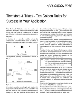
  • 1. APPLICATION NOTE Thyristors & Triacs - Ten Golden Rules for Success In Your Application. This Technical Publication aims to provide an interesting, descriptive and practical introduction to the golden rules that should be followed in the successful use of thyristors and triacs in power control applications. Thyristor A thyristor is a controlled rectifier where the unidirectional current flow from anode to cathode is initiated by a small signal current from gate to cathode. Fig. 1. Thyristor. The thyristor’s operating characteristic is shown in Fig. 2. Fig. 2. Thyristor V/I characteristic. Turn-on A thyristor is turned on by making its gate positive with respect to its cathode, thereby causing current flow into the gate. When the gate voltage reaches the threshold voltage VGT and the resulting current reaches the threshold current IGT, within a very short time known as the gate-controlled turn-on time, tgt, the load current can flow from ’a’ to ’k’. If the gate current consists of a very narrow pulse, say less than 1µs, its peak level will have to increase for progressively narrower pulse widths to guarantee triggering. When the load current reaches the thyristor’s latching current IL, load current flow will be maintained even after removal of the gate current. As long as adequate load current continues to flow, the thyristor will continue to conduct without the gate current. It is said to be latched ON. Note that the VGT, IGT and IL specifications given in data are at 25 ˚C. These parameters will increase at lower temperatures,sothedrivecircuitmust provide adequate voltage and current amplitude and duration for the lowest expected operating temperature. Rule 1. To turn a thyristor (or triac) ON, a gate current ≥ IGT must be applied until the load current is ≥ IL. This condition must be met at the lowest expected operating temperature. Sensitive gate thyristors such as the BT150 can be prone to turn-on by anode to cathode leakage current at high temperatures. If the junction temperature Tj is increased above Tj max, a point will be reached where the leakage current will be high enough to trigger the thyristor’s sensitive gate. It will then have lost its ability to remain in the blocking state and conduction will commence without the application of an external gate current. This methodofspurious turn-oncan beavoided byusing one or more of the following solutions: 1. Ensure that the temperature does not exceed Tj max. 2. Use a thyristor with a less sensitive gate such as the BT151, or reduce the existing thyristor’s sensitivity by including a gate-to-cathode resistor of 1kΩ or less. a k g On-state characteristic Off-state characteristic Avalanche breakdown region Reverse characteristic Reverse current Forward current Reverse voltage Forward voltage I L I H
  • 2. 3. If it is not possible to use a less sensitive thyristor due to circuit requirements, apply a small degree of reverse biasing to the gate during the ’off’ periods. This has the effect of increasing IL. During negative gate current flow, particularattention shouldbe paidto minimisingthegate power dissipation. Turn-off (commutation) In order to turn the thyristor off, the load current must be reduced below its holding current IH for sufficient time to allow all the mobile charge carriers to vacate the junction. This is achieved by "forced commutation" in DC circuits or at the end of the conducting half cycle in AC circuits. (Forced commutation is when the load circuit causes the load current to reduce to zero to allow the thyristor to turn off.) At this point, the thyristor will have returned to its fully blocking state. If the load current is not maintained below IH for long enough, the thyristor will not have returned to the fully blocking state by the time the anode-to-cathode voltage rises again. It might then return to the conducting state without an externally-applied gate current. Note that IH is also specified at room temperature and, likeIL,itreduces athighertemperatures.Thecircuitmust therefore allow sufficient time for the load current to fall below IH at the maximum expected operating temperature for successful commutation. Rule 2. To turn off (commutate) a thyristor (or triac), the load current must be < IH for sufficient time to allow a return to the blocking state. This condition must be met at the highest expected operating temperature. Triac A triac can be regarded as a "bidirectional thyristor" because it conducts in both directions. For standard triacs, current flow in either direction between the main terminals MT1 and MT2 is initiated by a small signal current applied between MT1 and the gate terminal. Fig. 3. Triac. Turn-on Unlike thyristors, standard triacs can be triggered by positive or negative current flow between the gate and MT1. (The rules for VGT, IGT and IL are the same as for thyristors. See Rule 1.) This permits triggering in four "quadrants" as summarised in Fig. 4. Fig. 4. Triac triggering quadrants. Fig. 5. Triac V/I characteristic. Where the gate is to be triggered by DC or unipolar pulses at zero-crossing of the load current, negative gate current is to be preferred for the following reasons. Theinternal construction of the triac means that the gate is more remote from the main current-carrying region when operating in the 3+ quadrant. This results in: 1. Higher IGT -> higher peak IG required, 2. Longer delay between IG and the commencement of load current flow -> longer duration of IG required, 3. Much lower dIT/dt capability -> progressive gate degradation can occur when controlling loads with high initial dI/dt (e.g. cold incandescent lamp filaments), 4. Higher IL (also true for 1- operation) -> longer IG duration might be needed for very small loads when conducting from the beginning of a mains half cycle to allow the load current to reach the higher IL. V MT2 V G 11 3 3 +- - + MT1 MT2+ G+ MT2+ G+ MT2- MT2- G- G- MT1 MT1 MT1 On-state Off-state Reverse current Forward current Reverse voltage Forward voltage I L I H L I H I T2- T2+ QUADRANT 1 QUADRANT 3 QUADRANT 2 QUADRANT 4 MT2 MT1 g
  • 3. In standard AC phase control circuits such as lamp dimmers and domestic motor speed controls, the gate and MT2 polarities are always the same. This means that operation is always in the 1+ and 3- quadrants where the triac’s switching parameters are the same. This results in symmetrical triac switching where the gate is at its most sensitive. Note:- The 1+ , 1- , 3- and 3+ notation for the four triggering quadrants is used for brevity instead of writing "MT2+, G+" for 1+ , etc. It is derived from the graph of the triac’s V/I characteristic. Positive MT2 corresponds with positive current flow into MT2, and vice versa (see Fig. 5). Hence, operation is in quadrants 1 and 3 only. The + and - superscripts refer to inward and outward gate current respectively. Rule 3. When designing a triac triggering circuit, avoid triggering in the 3+ quadrant (MT2-, G+) where possible. Alternative turn-on methods There are undesirable ways a triac can be turned on. Some are benign, while some are potentially destructive. (a) Noisy gate signal In electrically noisy environments, spurious triggering can occur if the noise voltage on the gate exceeds VGT and enough gate current flows to initiate regenerative action within the triac. The first line of defence is to minimise the occurrence of the noise in the first place. This is best achieved by keeping the gate connections as short as possible and ensuring that the common return from the gate drive circuit connects directly to the MT1 pin (or cathode in the case of a thyristor). In situations where the gate connections are hard wired, twisted pair wires or even shielded cable might be necessary to minimise pickup. Additional noise immunity can be provided by adding a resistor of 1kΩ or less between the gate and MT1 to reduce the gate sensitivity. If a high frequency bypass capacitor is also used, it is advisable to include a series resistor between it and the gate to minimise peak capacitor currents through the gate and minimise the possibilityofovercurrent damagetothetriac’sgate area. Alternatively, use a series H triac (e.g. BT139-600H). These are insensitive types with 10mA min IGT specs which are specifically designed to provide a high degree of noise immunity. Rule 4. To minimise noise pickup, keep gate connection length to a minimum. Take the return directly to MT1 (or cathode). If hard wired, use twisted pair or shielded cable. Fit a resistor of 1kΩ or less between gate and MT1. Fit a bypass capacitor in conjunction with a series resistor to the gate. Alternatively, use an insensitive series H triac. (b) Exceeding the max rate of change of commutating voltage dVCOM/dt This is most likely to occur when driving a highly reactive load where there is substantial phase shift between the load voltage and current waveforms. When the triac commutates as the load current passes through zero, the voltage will not be zero because of the phase shift (see Fig. 6). The triac is then suddenly required to block this voltage. The resulting rate of change of commutating voltage can force the triac back into conduction if it exceeds the permitted dVCOM/dt. This is because the mobile charge carriers have not been given time to clear the junction. The dVCOM/dt capability is affected by two conditions:- 1. The rate of fall of load current at commutation, dICOM/dt. Higher dICOM/dt lowers the dVCOM/dt capability. 2. The junction temperature Tj. Higher Tj lowers the dVCOM/dt capability. If the triac’s dVCOM/dt is likely to be exceeded, false triggering can be avoided by use of an RC snubber across MT1-MT2 to limit the rate of change of voltage. Common values are 100Ω carbon composition resistor, chosen for its surge current handling, and 100nF. Alternatively, use a Hi-Com triac. Note that the resistor should never be omitted from the snubber because therewould thenbe nothing to prevent the capacitor from dumping its charge into the triac and creating damaging dIT/dt during unfavourable turn-on conditions. Fig. 6. Triac dICOM/dt and dVCOM/dt. TimeOn-state voltage I V Reverse recovery current Re-applied Conducting current voltage dIcom/dt dVcom/dt
  • 4. (c) Exceeding the max rate of change of commutating current dICOM/dt Higher dICOM/dt is caused by higher load current, higher mains frequency (assuming sinewave current) or non sinewave load current. A well known cause of non sinewave load current and high dICOM/dt is rectifier-fed inductive loads. These can often result in commutation failurein standardtriacsas thesupplyvoltagefalls below the back EMF of the load and the triac current collapses suddenly to zero. The effect of this is illustrated in Fig. 7. During this condition of zero triac current, the load current will be "freewheeling" around the bridge rectifier circuit. Loads of this nature can generate such high dICOM/dt that the triac cannot support even the gentle reapplied dV/dt of a 50Hz waveform rising from zero volts. There will then be no benefit in adding a snubber across the triac because dVCOM/dt is not the problem. The dICOM/dt will have to be limited by adding an inductor of a few mH in series with the load. Alternatively, use a Hi-Com triac. Fig. 7. Effects of rectifier-fed inductive load on phase control circuit. (d) Exceeding the max rate of change of off-state voltage dVD/dt If a very high rate of change of voltage is applied across a non-conducting triac (or sensitive gate thyristor in particular) without exceeding its VDRM (see Fig. 8), internal capacitive current can generate enough gate current to trigger the device into conduction. Susceptibility is increased at high temperature. Where this is a problem, the dVD/dt must be limited by an RC snubber across MT1 and MT2 (or anode and cathode). In the case of triacs, using Hi-Com types can yield benefits. Fig. 8. Triac turn-on by exceeding dVD/dt. Rule 5. Where high dVD/dt or dVCOM/dt are likely to cause a problem, fit an RC snubber across MT1 and MT2. Where high dICOM/dt is likely to cause a problem, fit an inductor of a few mH in series with the load. Alternatively, use a Hi-Com triac. (e) Exceeding the repetitive peak off-state voltage VDRM If the MT2 voltage exceeds VDRM such as might occur during severe and abnormal mains transient conditions, MT2-MT1 leakage will reach a point where the triac will spontaneously break over into conduction (see Fig. 9). If theload permits high inrush currents toflow, extremely highlocalised current densitycan occur in thesmall area of silicon that is conducting. This can lead to burnout and destruction of the die. Incandescent lamps, capacitive loads and crowbar protection circuits are likely causes of high inrush currents. Turn-on by exceeding the triac’s VDRM or dVD/dt is not necessarily the main threat to its survival. It’s the dIT/dt that follows which is most likely to cause the damage. Due to the time required for conduction to spread out overthe wholejunction, the permitted dIT/dt is lower than if the triac is correctly turned on by a gate signal. If the dIT/dt can be limited during these conditions to this lower value, which is given in data, the triac is more likely to survive. This could be achievedby fitting a non saturable (air cored) inductor of a few µH in series with the load. If the above solution is unacceptable or impractical, an alternative solution would be to provide additional filtering and clamping to prevent the spikes reaching the triac. This would probably involve the use of a Metal Oxide Varistor as a "soft" voltage clamp across the supply, with series inductance followed by parallel capacitance upstream of the MOV. VD I T I G High dIcom/dt Commutation failure causes conduction at beginning of half cycle
  • 5. Fig. 9. Triac turn-on by exceeding VDRM. Doubts have been expressed by some manufacturers over the reliability of circuits which use MOVs across the mains, since they have been known to go into thermal runaway in high ambient temperatures and fail catastrophically. This is due to the fact that their operating voltage possesses a marked negative temperature coefficient. However, if the recommended voltage grade of 275V RMS is used for 230V mains, the risk of MOV failure should be negligible. Such failures are more likely if 250V RMS MOVs are used, which are underspecified for 230V RMS use at high ambient temperatures. Rule 6. Ifthetriac’sVDRM islikely tobeexceeded during severe mains transients, employ one of the following measures: Limit high dIT/dt with a non saturable inductor of a few µH in series with the load; Use a MOV across the mains in combination with filtering on the supply side. Turn-on dIT/dt When a triac or thyristor is triggered into conduction by the correct method via its gate, conduction begins in the die area immediately adjacent to the gate, then quickly spreads to cover the whole active area. This time delay imposes a limit on the permissible rate of rise of load current. A dIT/dt which is too high can cause localised burnout. An MT1-MT2 short will be the result. If triggering in the 3+ quadrant, an additional mechanism further reduces the permitted dIT/dt. It is possible to momentarily take the gate into reverse avalanche breakdownduringtheinitialrapid currentrise. This might not lead to immediate failure. Instead, there would be progressiveburnoutofthegate-MT1shorting resistance after repeated exposure. This would show itself by a progressive increase in IGT until the triac will no longer trigger. Sensitive triacs are likely to be the most susceptible. Hi-Com triacs are not affected as they do not operate in the 3+ quadrant. The dIT/dt capability is affected by how fast the gate current rises (dIG/dt) and the peak value of IG. Higher values of dIG/dt and peak IG (without exceeding the gate power ratings) give a higher dIT/dt capability. Rule 7. Healthy gate drive and avoiding 3+ operation maximises the triac’s dIT/dt capability. As mentioned previously, a common load with a high initial surge current is the incandescent lamp which has a low cold resistance. For resistive loads such as this, the dIT/dt would be at its highest if conduction commenced at a peak of the mains voltage. If this is likely to exceed the triac’s dIT/dt rating, it should be limited by the inclusion of an inductor of a few µH or even a Negative Temperature Coefficient thermistor in series with the load. Again, the inductor must not saturate during the maximum current peak. If it does, its inductance would collapse and it would no longer limit the dIT/dt. An air cored inductor meets the requirement. A more elegant solution which could avoid the requirement for a series current-limiting device would be to use zero voltage turn-on. This would allow the current to build up more gradually from the beginning of the sinewave. Note: It is important to rememember that zero voltage turn-on is only applicable to resistive loads. Using the same method for reactive loads where there is phase shift between voltage and current can cause "halfwaving" or unipolar conduction, leading to possible saturation of inductive loads, damagingly high peak currents and overheating. More advanced control employingzerocurrent switchingand / orvariabletrigger angle is required in this case. Rule 8. If the triac’s dIT/dt is likely to be exceeded, an air cored inductor of a few µH or an NTC thermistor should be fitted in series with the load. Alternatively, employ zero voltage turn-on for resistive loads. Turn-off Since triacs are used in AC circuits, they naturally commutate at the end of each half cycle of load current unless a gate signal is applied to maintain conduction from the beginning of the next half cycle. The rules for IH are the same as for the thyristor. See Rule 2. Hi-Com triac Hi-Com triacs have a different internal construction to conventional triacs. One of the differences is that the VD 200 400 600 800 1000 -200 -400 0 (V)
  • 6. two "thyristor halves" are better separated to reduce the influence that they have on each other. This has yielded two benefits: 1.Higher dVCOM/dt. This enables them to control reactive loads without the need for a snubber in most cases while still avoiding commutation failure. This reduces the component count, board size and cost, and eliminates snubber power dissipation. 2.Higher dICOM/dt.This drastically improves thechances of successfully commutating higher frequency or non sinewavecurrentswithouttheneedfor adICOM/dt-limiting inductor in series with the load. 3. Higher dVD/dt. Triacs become more sensitive at high operating temperatures. The higher dVD/dt of Hi-Com triacs reduces their tendency to spurious dV/dt turn-on when in the blocking state at high temperature. This enables them to be used in high temperature applications controlling resistive loads, such as cooking or heating applications, where conventional triacs could not be used. The different internal construction also means that 3+ triggering is not possible. This should not be a problem in the vast majority of cases because this is the least desirable and least used triggering quadrant, so direct substitution of a Hi-Com for an equivalent conventional triac will almost always be possible. Hi-Com triacs are fully described in two Philips Factsheets: Factsheet 013 - Understanding Hi-Com Triacs, and Factsheet 014 - Using Hi-Com Triacs. Triac mounting methods For small loads or very short duration load current (i.e. less than 1 second), it might be possible to operate the triac in free air. In most cases, however, it would be fixed to a heatsink or heat dissipating bracket. The three main methods of clamping the triac to a heatsinkare clip mounting,screw mounting and riveting. Mounting kits are available from many sources for the first two methods. Riveting is not a recommended method in most cases. Clip mounting This is the preferred method for minimum thermal resistance. The clip exerts pressure on the plastic body of the device. It is equally suitable for the non-isolated packages (SOT82 and SOT78) and the isolated packages (SOT186 F-pack and the more recent SOT186A X-pack). Note: SOT78 is otherwise known as TO220AB. Screw mounting 1. An M3 screw mounting kit for the SOT78 package includes a rectangular washer which shouldbe between the screw head and the tab. It should not exert any force on the plastic body of the device. 2. During mounting, the screwdriver blade should never exert force on the plastic body of the device. 3. The heatsink surface in contact with the tab should be deburred and flat to within 0.02mm in 10mm. 4. The mounting torque (with washer) should be between 0.55Nm and 0.8Nm. 5. Where an alternative exists, the use of self-tapping screws should be avoided due to the possible swelling oftheheatsinkmaterialaroundthefixinghole.This could be detrimental to the thermal contact between device and heatsink. (See 3 above.) The uncontrollable mounting torque is also a disadvantage with this fixing method. 6. The device should be mechanically fixed before the leads are soldered. This minimises undue stress on the leads. Riveting Pop riveting is not recommended unless great care is taken because the potentially severe forces resulting from such an operation can deform the tab and crack the die, rendering the device useless. In order to minimise rejects, the following rules should be obeyed if pop riveting: 1. The heatsink should present a flat, burr-free surface to the device. 2. The heatsink mounting hole diameter should be no greater than the tab mounting hole diameter. 3. The pop rivet should just be a clearance fit in the tab hole and heatsink mounting hole without free play. 4. The pop rivet should be fitted with its head, not the mandrel, on the tab side. 5. The pop rivet should be fitted at 90 degrees to the tab. (The rivet head should be in contact with the tab around its complete circumference.) 6. The head of the rivet should not be in contact with the plastic body of the device after riveting. 7. Mechanical fixing of the device and heatsink assembly to the PCB should be completed before the leads are soldered to minimise stressing of the leads. Rule 9. Avoid mechanical stress to the triac when fitting it to the heatsink. Fix, then solder. Never pop rivet with the rivet mandrel on the tab side.
  • 7. Thermal resistance Thermal resistance Rth is the resistance to the flow of heat away from the junction. It is analogous to electrical resistance; i.e. just as electrical resistance R = V/I, thermal resistance Rth = T/P, where T is the temperature rise in Kelvin and P is the power dissipation in Watts. Therefore Rth is expressed in K/W. For a device mounted vertically in free air, the thermal resistanceis dictated by thejunction-to-ambient thermal resistance Rth j-a. This is typically 100K/W for the SOT82 package, 60K/W for the SOT78 package and 55K/W for the isolated F-pack and X-pack. For a non isolated device mounted to a heatsink, the junction-to-ambient thermal resistance is the sum of the junction-to-mounting base, mounting base-to-heatsink and heatsink-to-ambient thermal resistances. Rth j-a = Rth j-mb + Rth mb-h + Rth h-a (non isolated package). The use of heat transfer compound or sheet between the device and heatsink is always recommended. In the case of isolated packages, there is no reference made to "mounting base", since the Rth mb-h is assumed to be constant and optimised with heat transfer compound. Therefore, the junction-to-ambient thermal resistance is the sum of the junction-to-heatsink and heatsink-to-ambient thermal resistances. Rth j-a = Rth j-h + Rth h-a (isolated package). Rth j-mb or Rth j-h are fixed and can be found in data for each device. Rth mb-h is also given in the mounting instructions for several options of insulated and non-insulated mounting, with or without heatsink compound. Rth h-a is governed by the heatsink size and the degree of unrestricted air movement past it. Calculation of heatsink size To calculate the required heatsink thermal resistance for a given triac and load current, we must first calculate the power dissipation in the triac using the following equation: P = Vo x IT(AVE) + Rs x IT(RMS) 2 . Knee voltage Vo and slope resistance Rs are obtained from the relevant VT graph in data book SC03. If the values are not already provided, they can be obtained from thegraph bydrawing a tangent tothe max VT curve. Thepoint on the VT axiswhere thetangent crosses gives Vo, while the slope of the tangent (VT/IT) gives Rs. Using the thermal resistance equation given above: Rth j-a = T/P. The max allowable junction temperature rise will be when Tj reaches Tj max in the highest ambient temperature. This gives us T. Rth j-a = Rth j-mb + Rth mb-h + Rth h-a. SC03 data gives us the values for Rth j-mb and Rth mb-h for our chosen mounting method, leaving Rth h-a as the only unknown. Thermal impedance The above calculations for thermal resistance are applicable to the steady state condition - that is for a duration greater than 1 second. This time is longenough for heat to flow from the junction to the heatsink. For current pulses or transients lasting for shorter than 1 second, however, heatsinking has progressively less effect. The heat is simply dissipated in the bulk of the devicewithvery littlereachingtheheatsink.For transient conditions such as these, the junction temperature rise is governed by the device’s junction-to-mounting base thermal impedance Zth j-mb. Zth j-mb decreases for decreasing current pulse duration due to reduced chip heating. As the duration increases towards 1 second, Zth j-mb increases to the steady state Rth j-mb value. The Zth j-mb curve for bidirectional and unidirectional current down to 10µs duration is shown for each device in the SC03 data book. Rule For longterm reliability, ensure that the Rth j-a 10. islow enoughtokeep thejunction temperature within Tj max for the highest expected ambient temperature. Range and packaging Philips thyristors range from 0.8A in SOT54 (TO92) to 25A in SOT78 (TO220AB). Philips triacs range from 1A in SOT223 to25A in SOT78. Conventional types (4-quadrant triggering) and Hi-Com types (3-quadrant triggering) are available. SOT54 types are planned for 1996. The smallest package is the surface mount SOT223 for the smaller thyristors and triacs (Fig. 10). The power dissipation is governed by the degree of heatsinking offered by the PCB onto which it is soldered. The same respective chips are also available in SOT82 which is a non isolated package (Fig. 12). The improved heat removal of this package when heatsunk allows higher current ratings and improved power dissipations. Figure 11 shows SOT54 in which the very smallest devices are mounted. Smaller chips than those accommodated by SOT223 go into this package, which offers the most compact non surface mount solution.
  • 8. SOT78 is the most common non isolated package in which most of our devices are supplied (Fig. 13). Figure 14 shows SOT186 (F-pack). This has been the traditional Philips isolated package. It offers an isolation voltage of 1,500V peak between device and heatsink under clean conditions. The more recent SOT186A package (X-pack) shown in Fig. 15 possesses several advantages over the older type. 1. It has the same dimensions as the SOT78 package for pin spacing from the mounting surface, so it can directly replace SOT78 devices to provide isolation without the need for modification of the mounting arrangement. 2. It has no exposed metal at the top of the tab, and creepage distances from pins to heatsink are greater, so it can offer an improved true isolation of 2,500V RMS. 3. It is a fully encapsulated SOT78 replacement. Fig. 10. SOT223. handbook, full pagewidth 6.7 6.3 0.95 0.85 2.3 0.80 0.60 4.6 3.1 2.9 3.7 3.3 7.3 6.7 A B 0.2 A 1.80 max 1616o max 10o max 0.10 0.01 0.32 0.24 4 1 2 3 MSA035 - 1 (4x) 0.1 BM M S seating plane 0.1 S o Fig. 11. SOT54 (TO92). MBC015 - 1 2.54 4.8 max 4.2 max 1.6 0.66 0.56 1 2 3 5.2 max 12.7 min 2.5 max (1) 0.48 0.40 0.40 min
  • 9. Fig. 12. SOT82. 1/1 page = 296 mm (Datasheet) 27 mm 0.88 max 2.29 1 2 3 3.75 11.1 max 15.3 min 3.1 2.5 7.8 max 2.8 2.3 2.54 max (1) 1.2 4.58 0.5 MSA286 Fig. 13. SOT78 (TO220AB). 5.9 min 1.3 4.5 max 15.8 max 10.3 max 3.7 2.8 3.0 13.5 min 3.0 max not tinned 1.3 max (2x) 0.6 2.4 2.54 2.54 0.9 max (3x) MSA060 - 1 1 2 3
  • 10. Fig. 14. SOT186 F-pack. MBC667 4.4 max 2.9 max 7.9 7.5 17 max 13.5 min 0.55 max 1.3 3.2 3.0 5.7 max 10.2 max 4.4 4.0 0.9 0.5 3.5 max not tinned dimensions within this zone are uncontrolled 4.4 seating plane1.5 max 1 2 3 0.9 0.7 M0.4 2.54 5.08 Fig. 15. SOT186A X-pack. recesses O 2.5 x 0.8 max depth (2x) 10.3 max 3.2 3.0 4.6 max 2.9 max 6.4 15.8 max19 max 3 max untinned dimensions within this zone are uncontrolled 2.5 3 13.5 min 5.08 2.54 2.8 0.6 0.5 2.5 seating plane 0.4 M 1 2 3 1.0 (2x) 1.3 0.9 0.7 MSA178
  • 11. The Ten Golden Rules Summarised Rule 1. To turn a thyristor (or triac) ON, a gate current ≥ IGT must be applied until the load current is ≥ IL. This condition must be met at the lowest expected operating temperature. Rule 2. To turn off (commutate) a thyristor (or triac), the load current must be < IH for sufficient time to allow a return to the blocking state. This condition must be met at the highest expected operating temperature. Rule 3. When designing a triac triggering circuit, avoid triggering in the 3+ quadrant (MT2-, G+) where possible. Rule 4. To minimise noise pickup, keep gate connection length to a minimum. Take the return directly to MT1 (or cathode). If hard wired, use twisted pair or shielded cable. Fit a resistor of 1kΩ or less between gate and MT1. Fit a bypass capacitor in conjunction with a series resistor to the gate. Alternatively, use an insensitive series H triac. Rule 5. Where high dVD/dt or dVCOM/dt are likely to cause a problem, fit an RC snubber across MT1 and MT2. Where high dICOM/dt is likely to cause a problem, fit an inductor of a few mH in series with the load. Alternatively, use a Hi-Com triac. Rule 6. If the triac’s VDRM is likely to be exceeded during severe mains transients, employ one of the following measures: Limit high dIT/dt with a non saturable inductor of a few µH in series with the load; Use a MOV across the mains in combination with filtering on the supply side. Rule 7. Healthy gate drive and avoiding 3+ operation maximises the triac’s dIT/dt capability. Rule 8. If the triac’s dIT/dt is likely to be exceeded, an air cored inductor of a few µH or an NTC thermistor should be fitted in series with the load. Alternatively, employ zero voltage turn-on for resistive loads. Rule 9. Avoid mechanical stress to the triac when fitting it to the heatsink. Fix, then solder. Never pop rivet with the rivet mandrel on the tab side. Rule 10. For longterm reliability, ensure that the Rth j-a is low enough to keep the junction temperature within Tj max for the highest expected ambient temperature.