
Recomendados
Más contenido relacionado
Similar a datasheet.pdf
Similar a datasheet.pdf (20)
Último
Último (12)
datasheet.pdf
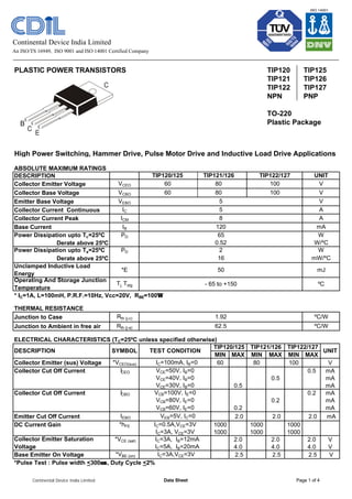
- 1. PLASTIC POWER TRANSISTORS TIP120 TIP125 TIP121 TIP126 TIP122 TIP127 NPN PNP TO-220 Plastic Package High Power Switching, Hammer Drive, Pulse Motor Drive and Inductive Load Drive Applications ABSOLUTE MAXIMUM RATINGS DESCRIPTION Collector Emitter Voltage VCEO Collector Base Voltage VCBO Emitter Base Voltage VEBO Collector Current Continuous IC Collector Current Peak ICM Base Current IB Power Dissipation upto Tc=25ºC PD Derate above 25ºC Power Dissipation upto Ta=25ºC PD Derate above 25ºC * IC=1A, L=100mH, P.R.F.=10Hz, Vcc=20V, RBE=100Ω Ω THERMAL RESISTANCE Junction to Case Rth (j-c) Junction to Ambient in free air Rth (j-a) ELECTRICAL CHARACTERISTICS (TC=25ºC unless specified otherwise) MIN MAX MIN MAX MIN MAX Collector Emitter (sus) Voltage *VCEO(sus) IC=100mA, IB=0 60 80 100 V Collector Cut Off Current ICEO VCE=50V, IB=0 0.5 mA VCE=40V, IB=0 0.5 mA VCE=30V, IB=0 0.5 mA Collector Cut Off Current ICBO VCB=100V, IE=0 0.2 mA VCB=80V, IE=0 0.2 mA VCB=60V, IE=0 0.2 mA Emitter Cut Off Current IEBO VEB=5V, IC=0 2.0 2.0 2.0 mA DC Current Gain *hFE IC=0.5A,VCE=3V 1000 1000 1000 IC=3A, VCE=3V 1000 1000 1000 *VCE (sat) IC=3A, IB=12mA 2.0 2.0 2.0 V IC=5A, IB=20mA 4.0 4.0 4.0 V Base Emitter On Voltage *VBE (on) IC=3A,VCE=3V 2.5 2.5 2.5 V *Pulse Test : Pulse width <300µ µs, Duty Cycle <2% Unclamped Inductive Load Energy - 65 to +150 5 5 8 120 65 0.52 2 16 W/ºC W mW/ºC ºC ºC/W *E Collector Emitter Saturation Voltage A A mA W UNIT V V V ºC/W TIP122/127 TIP121/126 TIP120/125 UNIT Operating And Storage Junction Temperature Tj, Tstg DESCRIPTION SYMBOL TEST CONDITION TIP120/125 TIP121/126 60 80 60 80 100 TIP122/127 100 mJ 50 1.92 62.5 Continental Device India Limited Data Sheet Page 1 of 4 Continental Device India Limited An ISO/TS 16949, ISO 9001 and ISO 14001 Certified Company
- 2. PLASTIC POWER TRANSISTORS TIP120 TIP125 TIP121 TIP126 TIP122 TIP127 NPN PNP TO-220 Plastic Package ELECTRICAL CHARACTERISTICS (TC=25ºC unless specified otherwise) DYNAMIC CHARACTERISTIC DESCRIPTION SYMBOL TEST CONDITION MIN TYP MAX Output Capacitance Cob VCB=10V, IE=0, f=0.1MHz TIP125,126,127 300 TIP120,121,122 200 SWITCHING CHARACTERISTICS DESCRIPTION SYMBOL TEST CONDITION MIN TYP MAX Turn on time ton IC=3A, RL=10Ω 0.4 IB1=IB2=12mA Turn off time toff VEB (off)=5V 1.2 Small Signal Current Gain IC=3A,VCE=4V, f=1MHz 4 UNIT UNIT hfe µs µs pF pF Continental Device India Limited Data Sheet Page 2 of 4
- 3. TIP120 TIP125 TIP121 TIP126 TIP122 TIP127 NPN PNP TO-220 Plastic Package TO-220 Plastic Package TO-220 Tube Packing TO-220 /FP 200 pcs/ polybag 50 pcs/ tube 396 gm/ 200 pcs 120 gm/ 50 pcs 3"x7.5"x7.5" 3.5"x3.7"x21.5" 1.0K 1.0K 17"x15"x13.5" 19" x 19" x 19" 16.0K 10.0K 36 kgs 29 kgs PACKAGE Net Weight/ Qty Details STANDARD PACK INNER CARTON BOX Qty OUTER CARTON BOX Qty GrWt Size Size Packing Detail Pin Configuration 1. Base 2. Collector 3. Emitter 4. Collector 3 2 1 4 All diminsions in mm. DIM MIN MAX N O B C D — E F G H J K L M A 14.42 16.51 9.63 10.67 3.56 4.83 0.90 1.15 1.40 3.75 3.88 2.29 2.79 2.54 3.43 — 0.56 12.70 14.73 2.80 4.07 2.03 2.92 — 31.24 7 DEG B F C E H L N K 1 2 3 D G M J A 0 0 6.87 32.85 13.74 End Pin Tube Thickness DEVICE NAME Label 536.00 ±1.5 50 Pcs./Tube Sr. QTY. All Dimensions in mm AMMO PACK SIZE 20 Tubes/Ammo Pack 1000 Pcs./Ammo Pack Label 538.00 75.0 92.0 Continental Device India Limited Data Sheet Page 3 of 4
- 4. Notes TIP120 TIP125 TIP121 TIP126 TIP122 TIP127 NPN PNP TO-220 Plastic Package TIP120_127Rev 311002E Disclaimer The product information and the selection guides facilitate selection of the CDIL's Discrete Semiconductor Device(s) best suited for application in your product(s) as per your requirement. It is recommended that you completely review our Data Sheet(s) so as to confirm that the Device(s) meet functionality parameters for your application. The information furnished in the Data Sheet and on the CDIL Web Site/CD are believed to be accurate and reliable. CDIL however, does not assume responsibility for inaccuracies or incomplete information. Furthermore, CDIL does not assume liability whatsoever, arising out of the application or use of any CDIL product; neither does it convey any license under its patent rights nor rights of others. These products are not designed for use in life saving/support appliances or systems. CDIL customers selling these products (either as individual Discrete Semiconductor Devices or incorporated in their end products), in any life saving/support appliances or systems or applications do so at their own risk and CDIL will not be responsible for any damages resulting from such sale(s). CDIL strives for continuous improvement and reserves the right to change the specifications of its products without prior notice. CDIL is a registered Trademark of Continental Device India Limited C-120 Naraina Industrial Area, New Delhi 110 028, India. Telephone + 91-11-2579 6150, 5141 1112 Fax + 91-11-2579 5290, 5141 1119 email@cdil.com www.cdilsemi.com Continental Device India Limited Data Sheet Page 4 of 4