SlideShare una empresa de Scribd logo
1 de 40
Descargar para leer sin conexión
Fundamentals of Power Electronics Chapter 15: Transformer design1
Chapter 15 Transformer Design
Some more advanced design issues, not considered in previous
chapter:
• Inclusion of core loss
• Selection of operating flux
density to optimize total loss
• Multiple winding design: as in
the coupled-inductor case,
allocate the available window
area among several windings
• A transformer design
procedure
• How switching frequency
affects transformer size
n1 : n2
: nk
R1 R2
Rk
+
v1(t)
–
+
v2(t)
–
+
vk(t)
–
i1(t) i2(t)
ik(t)
Fundamentals of Power Electronics Chapter 15: Transformer design2
Chapter 15 Transformer Design
15.1 Transformer design: Basic constraints
15.2 A step-by-step transformer design procedure
15.3 Examples
15.4 AC inductor design
15.5 Summary
Fundamentals of Power Electronics Chapter 15: Transformer design3
15.1 Transformer Design:
Basic Constraints
Core loss
Typical value of for ferrite materials: 2.6 or 2.7
B is the peak value of the ac component of B(t), i.e., the peak ac flux
density
So increasing B causes core loss to increase rapidly
This is the first constraint
Pfe = K fe(∆B)β
Ac lm
Fundamentals of Power Electronics Chapter 15: Transformer design4
Flux density
Constraint #2
Flux density B(t) is related to the
applied winding voltage according
to Faraday’s Law. Denote the volt-
seconds applied to the primary
winding during the positive portion
of v1(t) as 1:
λ1 = v1(t)dt
t1
t2
This causes the flux to change from
its negative peak to its positive peak.
From Faraday’s law, the peak value
of the ac component of flux density is
To attain a given flux density,
the primary turns should be
chosen according to
area λ1
v1(t)
t1 t2 t
∆B =
λ1
2n1Ac
n1 =
λ1
2∆BAc
Fundamentals of Power Electronics Chapter 15: Transformer design5
Copper loss
Constraint #3
• Allocate window area between windings in optimum manner, as
described in previous section
• Total copper loss is then equal to
Pcu =
ρ(MLT)n1
2
Itot
2
WAKu
Itot =
nj
n1
IjΣj = 1
k
with
Eliminate n1, using result of previous slide:
Note that copper loss decreases rapidly as B is increased
Pcu =
ρλ1
2
Itot
2
4Ku
(MLT)
WAAc
2
1
∆B
2
Fundamentals of Power Electronics Chapter 15: Transformer design6
Total power loss
4. Ptot = Pcu + Pfe
Ptot = Pfe + Pcu
There is a value of B
that minimizes the total
power loss
Pcu =
ρλ1
2
Itot
2
4Ku
(MLT)
WAAc
2
1
∆B
2
Pfe = K fe(∆B)β
Ac lm
∆B
Power
loss
Ptot
CopperlossPcu
CorelossP
fe
Optimum ∆B
Fundamentals of Power Electronics Chapter 15: Transformer design7
5. Find optimum flux density B
Ptot = Pfe + Pcu
Given that
Then, at the B that minimizes Ptot, we can write
Note: optimum does not necessarily occur where Pfe = Pcu. Rather, it
occurs where
dPtot
d(∆B)
=
dPfe
d(∆B)
+
dPcu
d(∆B)
= 0
dPfe
d(∆B)
= –
dPcu
d(∆B)
Fundamentals of Power Electronics Chapter 15: Transformer design8
Take derivatives of core and copper loss
Now, substitute into and solve for B:
Optimum B for a
given core and
application
Pcu =
ρλ1
2
Itot
2
4Ku
(MLT)
WAAc
2
1
∆B
2
Pfe = K fe(∆B)β
Ac lm
dPfe
d(∆B)
= βK fe(∆B) β – 1
Aclm dPcu
d(∆B)
= – 2
ρλ1
2
Itot
2
4Ku
(MLT)
WAAc
2 (∆B)– 3
dPfe
d(∆B)
= –
dPcu
d(∆B)
∆B =
ρλ1
2
Itot
2
2Ku
(MLT)
WAAc
3
lm
1
βK fe
1
β + 2
Fundamentals of Power Electronics Chapter 15: Transformer design9
Total loss
Substitute optimum B into expressions for Pcu and Pfe. The total loss is:
Rearrange as follows:
Left side: terms depend on core
geometry
Right side: terms depend on
specifications of the application
Ptot = AclmK fe
2
β + 2
ρλ1
2
Itot
2
4Ku
(MLT)
WAAc
2
β
β + 2
β
2
–
β
β + 2
+
β
2
2
β + 2
WA Ac
2(β – 1)/β
(MLT)lm
2/β
β
2
–
β
β + 2
+
β
2
2
β + 2
–
β + 2
β
=
ρλ1
2
Itot
2
K fe
2/β
4Ku Ptot
β + 2 /β
Fundamentals of Power Electronics Chapter 15: Transformer design10
The core geometrical constant Kgfe
Define
Design procedure: select a core that satisfies
Appendix D lists the values of Kgfe for common ferrite cores
Kgfe is similar to the Kg geometrical constant used in Chapter 14:
• Kg is used when Bmax is specified
• Kgfe is used when B is to be chosen to minimize total loss
Kgfe =
WA Ac
2(β – 1)/β
(MLT)lm
2/β
β
2
–
β
β + 2
+
β
2
2
β + 2
–
β + 2
β
Kgfe ≥
ρλ1
2
Itot
2
K fe
2/β
4Ku Ptot
β + 2 /β
Fundamentals of Power Electronics Chapter 15: Transformer design11
15.2 Step-by-step
transformer design procedure
The following quantities are specified, using the units noted:
Wire effective resistivity ( -cm)
Total rms winding current, ref to pri Itot (A)
Desired turns ratios n2/n1, n3/n1, etc.
Applied pri volt-sec 1 (V-sec)
Allowed total power dissipation Ptot (W)
Winding fill factor Ku
Core loss exponent
Core loss coefficient Kfe (W/cm3T )
Other quantities and their dimensions:
Core cross-sectional area Ac (cm2)
Core window area WA (cm2)
Mean length per turn MLT (cm)
Magnetic path length le (cm)
Wire areas Aw1, … (cm2)
Peak ac flux density B (T)
Fundamentals of Power Electronics Chapter 15: Transformer design12
Procedure
1. Determine core size
Select a core from Appendix D that satisfies this inequality.
It may be possible to reduce the core size by choosing a core material
that has lower loss, i.e., lower Kfe.
Kgfe ≥
ρλ1
2
Itot
2
K fe
2/β
4Ku Ptot
β + 2 /β
108
Fundamentals of Power Electronics Chapter 15: Transformer design13
2. Evaluate peak ac flux density
At this point, one should check whether the saturation flux density is
exceeded. If the core operates with a flux dc bias Bdc, then B + Bdc
should be less than the saturation flux density Bsat.
If the core will saturate, then there are two choices:
• Specify B using the Kg method of Chapter 14, or
• Choose a core material having greater core loss, then repeat
steps 1 and 2
∆B = 108 ρλ1
2
Itot
2
2Ku
(MLT)
WAAc
3
lm
1
βK fe
1
β + 2
Fundamentals of Power Electronics Chapter 15: Transformer design14
3. and 4. Evaluate turns
Primary turns:
Choose secondary turns according to
desired turns ratios:
n2 = n1
n2
n1
n3 = n1
n3
n1
n1 =
λ1
2∆BAc
104
Fundamentals of Power Electronics Chapter 15: Transformer design15
5. and 6. Choose wire sizes
α1 =
n1I1
n1Itot
α2 =
n2I2
n1Itot
αk =
nkIk
n1Itot
Fraction of window area
assigned to each winding:
Choose wire sizes according
to:
Aw1 ≤
α1KuWA
n1
Aw2 ≤
α2KuWA
n2
Fundamentals of Power Electronics Chapter 15: Transformer design16
Check: computed transformer model
iM, pk =
λ1
2LM
R1 =
ρn1(MLT)
Aw1
R2 =
ρn2(MLT)
Aw2
Predicted magnetizing
inductance, referred to primary:
Peak magnetizing current:
Predicted winding resistances:
n1 : n2
: nk
R1 R2
Rk
i1(t) i2(t)
ik(t)
LM
iM(t)
LM =
µn1
2
Ac
lm
Fundamentals of Power Electronics Chapter 15: Transformer design17
15.4.1 Example 1: Single-output isolated
Cuk converter
100 W fs = 200 kHz
D = 0.5 n = 5
Ku = 0.5 Allow Ptot = 0.25 W
Use a ferrite pot core, with Magnetics Inc. P material. Loss
parameters at 200 kHz are
Kfe = 24.7 = 2.6
+
–
+
V
5 V
–
Vg
25 V
n : 1
I
20 A
Ig
4 A
+
v2(t)
–
–
v1(t)
+
i1(t) i2(t)
– vC2(t) ++ vC1(t) –
Fundamentals of Power Electronics Chapter 15: Transformer design18
Waveforms
v1(t)
i1(t)
i2(t)
DTs
Area λ1VC1
– nVC2
D'Ts
I/n
– Ig
I
– nIg
Applied primary volt-
seconds:
λ1 = DTsVc1 = (0.5) (5 µsec ) (25 V)
= 62.5 V–µsec
Applied primary rms
current:
I1 = D I
n
2
+ D' Ig
2
= 4 A
Applied secondary rms
current:
I2 = nI1 = 20 A
Total rms winding
current:
Itot = I1 + 1
n I2 = 8 A
Fundamentals of Power Electronics Chapter 15: Transformer design19
Choose core size
Kgfe ≥
(1.724⋅10– 6
)(62.5⋅10– 6
)2
(8)2
(24.7) 2/2.6
4 (0.5) (0.25) 4.6/2.6
108
= 0.00295
Pot core data of Appendix D lists 2213 pot core with
Kgfe = 0.0049
Next smaller pot core is not large enough.
Fundamentals of Power Electronics Chapter 15: Transformer design20
Evaluate peak ac flux density
This is much less than the saturation flux density of approximately
0.35 T. Values of B in the vicinity of 0.1 T are typical for ferrite
designs that operate at frequencies in the vicinity of 100 kHz.
∆B = 108 (1.724⋅10– 6
)(62.5⋅10– 6
)2
(8)2
2 (0.5)
(4.42)
(0.297)(0.635)3
(3.15)
1
(2.6)(24.7)
1/4.6
= 0.0858 Tesla
Fundamentals of Power Electronics Chapter 15: Transformer design21
Evaluate turns
n1 = 104 (62.5⋅10– 6
)
2(0.0858)(0.635)
= 5.74 turns
n2 =
n1
n = 1.15 turns
In practice, we might select
n1 = 5 and n2 = 1
This would lead to a slightly higher flux density and slightly higher
loss.
Fundamentals of Power Electronics Chapter 15: Transformer design22
Determine wire sizes
Fraction of window area allocated to each winding:
α1 =
4 A
8 A
= 0.5
α2 =
1
5 20 A
8 A
= 0.5
(Since, in this example, the ratio of
winding rms currents is equal to the
turns ratio, equal areas are
allocated to each winding)
Wire areas:
Aw1 =
(0.5)(0.5)(0.297)
(5)
= 14.8⋅10– 3
cm2
Aw2 =
(0.5)(0.5)(0.297)
(1)
= 74.2⋅10– 3
cm2
From wire table,
Appendix D:
AWG #16
AWG #9
Fundamentals of Power Electronics Chapter 15: Transformer design23
Wire sizes: discussion
Primary
5 turns #16 AWG
Secondary
1 turn #9 AWG
• Very large conductors!
• One turn of #9 AWG is not a practical solution
Some alternatives
• Use foil windings
• Use Litz wire or parallel strands of wire
Fundamentals of Power Electronics Chapter 15: Transformer design24
Effect of switching frequency on transformer size
for this P-material Cuk converter example
0
0.02
0.04
0.06
0.08
0.1
Switching frequency
Bmax,Tesla
Potcoresize
4226
3622
2616
2213
1811 1811
2213
2616
25 kHz 50 kHz 100 kHz 200 kHz 250 kHz 400 kHz 500 kHz 1000 kHz
• As switching frequency is
increased from 25 kHz to
250 kHz, core size is
dramatically reduced
• As switching frequency is
increased from 400 kHz to
1 MHz, core size
increases
Fundamentals of Power Electronics Chapter 15: Transformer design25
15.3.2 Example 2
Multiple-Output Full-Bridge Buck Converter
Switching frequency 150 kHz
Transformer frequency 75 kHz
Turns ratio 110:5:15
Optimize transformer at D = 0.75
: n2
+
v1(t)
–
+
–
D1
Q1
D2Q2
D3
Q3
D4Q4
i1(t)
+
5 V
–
D5
D6
I5V
100 Ai2a(t)
+
15 V
–
D7
D8
i3a(t)
n1 :
: n2
: n3
: n3
i2b(t)
i2b(t)
I15V
15 A
T1
Vg
160 V
Fundamentals of Power Electronics Chapter 15: Transformer design26
Other transformer design details
Use Magnetics, Inc. ferrite P material. Loss parameters at 75 kHz:
Kfe = 7.6 W/T cm3
= 2.6
Use E-E core shape
Assume fill factor of
Ku = 0.25 (reduced fill factor accounts for added insulation required
in multiple-output off-line application)
Allow transformer total power loss of
Ptot = 4 W (approximately 0.5% of total output power)
Use copper wire, with
= 1.724·10–6 -cm
Fundamentals of Power Electronics Chapter 15: Transformer design27
Applied transformer waveforms
t
i2a(t)
0
i3a(t)
0 DTs
Ts
2Ts
Ts
+DTs
i1(t)
0
v1(t)
0 0
Vg
– Vg
Area λ1
= Vg DTs
n2
n1
I5V +
n3
n1
I15V
–
n2
n1
I5V +
n3
n1
I15V
I5V
0.5I5V
I15V
0.5I15V
0
: n2
+
v1(t)
–
D3
D4
i1(t)
D5
D6
i2a(t)
D7
D8
i3a(t)
n1 :
: n2
: n3
: n3
i2b(t)
i2b(t)
T1
Fundamentals of Power Electronics Chapter 15: Transformer design28
Applied primary volt-seconds
v1(t)
0 0
Vg
– Vg
Area λ1
= Vg DTs
λ1 = DTsVg = (0.75) (6.67 µsec ) (160 V) = 800 V–µsec
Fundamentals of Power Electronics Chapter 15: Transformer design29
Applied primary rms current
i1(t)
0
n2
n1
I5V +
n3
n1
I15V
–
n2
n1
I5V +
n3
n1
I15V
I1 =
n2
n1
I5V +
n3
n1
I15V D = 5.7 A
Fundamentals of Power Electronics Chapter 15: Transformer design30
Applied rms current, secondary windings
t
i2a(t)
0
i3a(t)
0 DTs Ts 2TsTs+DTs
I5V
0.5I5V
I15V
0.5I15V
0
I3 = 1
2 I15V 1 + D = 9.9 A
I2 = 1
2 I5V 1 + D = 66.1 A
Fundamentals of Power Electronics Chapter 15: Transformer design31
Itot
RMS currents, summed over all windings and referred to primary
Itot =
nj
n1
IjΣall 5
windings
= I1 + 2
n2
n1
I2 + 2
n3
n1
I3
= 5.7 A + 5
110
66.1 A + 15
110
9.9 A
= 14.4 A
Fundamentals of Power Electronics Chapter 15: Transformer design32
Select core size
Kgfe ≥
(1.724⋅10– 6
)(800⋅10– 6
)2
(14.4)2
(7.6) 2/2.6
4 (0.25) (4) 4.6/2.6
108
= 0.00937
A
From Appendix D
Fundamentals of Power Electronics Chapter 15: Transformer design33
Evaluate ac flux density B
Bmax = 108 ρλ1
2
Itot
2
2Ku
(MLT)
WAAc
3
lm
1
βK fe
1
β + 2
Eq. (15.20):
Plug in values:
This is less than the saturation flux density of approximately 0.35 T
∆B = 108 (1.724⋅10– 6
)(800⋅10– 6
)2
(14.4)2
2(0.25)
(8.5)
(1.1)(1.27)3
(7.7)
1
(2.6)(7.6)
1/4.6
= 0.23 Tesla
Fundamentals of Power Electronics Chapter 15: Transformer design34
Evaluate turns
Choose n1 according to Eq. (15.21):
n1 = 104 (800⋅10– 6
)
2(0.23)(1.27)
= 13.7 turns
Choose secondary turns
according to desired turns ratios:
n2 =
5
110
n1 = 0.62 turns
n3 =
15
110
n1 = 1.87 turns
Rounding the number of turns
To obtain desired turns ratio
of
110:5:15
we might round the actual
turns to
22:1:3
Increased n1 would lead to
• Less core loss
• More copper loss
• Increased total loss
n1 =
λ1
2∆BAc
104
Fundamentals of Power Electronics Chapter 15: Transformer design35
Loss calculation
with rounded turns
With n1 = 22, the flux density will be reduced to
The resulting losses will be
Pfe = (7.6)(0.143)2.6
(1.27)(7.7) = 0.47 W
Pcu =
(1.724⋅10– 6
)(800⋅10– 6
)2
(14.4)2
4 (0.25)
(8.5)
(1.1)(1.27)2
1
(0.143)2 108
= 5.4 W
Ptot = Pfe + Pcu = 5.9 W
Which exceeds design goal of 4 W by 50%. So use next larger core
size: EE50.
∆B =
(800⋅10– 6
)
2(22)(1.27)
104
= 0.143 Tesla
Fundamentals of Power Electronics Chapter 15: Transformer design36
Calculations with EE50
Repeat previous calculations for EE50 core size. Results:
B = 0.14 T, n1 = 12, Ptot = 2.3 W
Again round n1 to 22. Then
B = 0.08 T, Pcu = 3.89 W, Pfe = 0.23 W, Ptot = 4.12 W
Which is close enough to 4 W.
Fundamentals of Power Electronics Chapter 15: Transformer design37
Wire sizes for EE50 design
Aw1 =
α1KuWA
n1
=
(0.396)(0.25)(1.78)
(22)
= 8.0⋅10– 3
cm2
⇒ AWG #19
Aw2 =
α2KuWA
n2
=
(0.209)(0.25)(1.78)
(1)
= 93.0⋅10– 3
cm2
⇒ AWG #8
Aw3 =
α3KuWA
n3
=
(0.094)(0.25)(1.78)
(3)
= 13.9⋅10– 3
cm2
⇒ AWG #16
α1 =
I1
Itot
= 5.7
14.4
= 0.396
α2 =
n2I2
n1Itot
= 5
110
66.1
14.4
= 0.209
α3 =
n3I3
n1Itot
= 15
110
9.9
14.4
= 0.094
Window allocations Wire gauges
Might actually use foil or Litz wire for secondary windings
Fundamentals of Power Electronics Chapter 15: Transformer design38
Discussion: Transformer design
• Process is iterative because of round-off of physical number of
turns and, to a lesser extent, other quantities
• Effect of proximity loss
– Not included in design process yet
– Requires additional iterations
• Can modify procedure as follows:
– After a design has been calculated, determine number of layers in
each winding and then compute proximity loss
– Alter effective resistivity of wire to compensate: define
eff = Pcu/Pdc where Pcu is the total copper loss (including proximity
effects) and Pdc is the copper loss predicted by the dc resistance.
– Apply transformer design procedure using this effective wire
resistivity, and compute proximity loss in the resulting design.
Further iterations may be necessary if the specifications are not
met.
Fundamentals of Power Electronics Chapter 15: Transformer design39
15.4 AC Inductor Design
+
v(t)
–
L
i(t) Core
Window area WA
Core mean length
per turn (MLT)
Wire resistivity ρ
Fill factor Ku
Air gap
lg
n
turns
Core area
Ac
Area λ
v(t)
t1 t2 t
i(t)
Design a single-winding inductor, having
an air gap, accounting for core loss
(note that the previous design procedure of
this chapter did not employ an air gap, and
inductance was not a specification)
Fundamentals of Power Electronics Chapter 15: Transformer design40
Outline of key equations
L =
µ0Acn2
lg
∆B = λ
2nAc
Obtain specified inductance:
Relationship between
applied volt-seconds and
peak ac flux density:
Pcu =
ρn2(MLT)
KuWA
I2
Copper loss (using dc
resistance):
∆B =
ρλ2
I2
2Ku
(MLT)
WAAc
3
lm
1
βK fe
1
β + 2
Total loss is minimized when
Kgfe ≥
ρλ2
I2
K fe
2/β
2Ku Ptot
β + 2 /β
Must select core that satisfies
See Section 15.4.2 for step-by-step
design equations

Más contenido relacionado

La actualidad más candente

Chapter 14
Chapter 14Chapter 14
Chapter 14Tha Mike
 
Chapter 05
Chapter 05Chapter 05
Chapter 05Tha Mike
 
Chapter 01
Chapter 01Chapter 01
Chapter 01Tha Mike
 
Chapter 17
Chapter 17Chapter 17
Chapter 17Tha Mike
 
Chapter 20
Chapter 20Chapter 20
Chapter 20Tha Mike
 
Chapter 16
Chapter 16Chapter 16
Chapter 16Tha Mike
 
Journal On LDO From IJEETC
Journal On LDO From IJEETCJournal On LDO From IJEETC
Journal On LDO From IJEETCSadanand Patil
 
IC Design of Power Management Circuits (I)
IC Design of Power Management Circuits (I)IC Design of Power Management Circuits (I)
IC Design of Power Management Circuits (I)Claudia Sin
 
Ee6378 bandgap reference
Ee6378 bandgap referenceEe6378 bandgap reference
Ee6378 bandgap referencessuser2038c9
 
IC Design of Power Management Circuits (IV)
IC Design of Power Management Circuits (IV)IC Design of Power Management Circuits (IV)
IC Design of Power Management Circuits (IV)Claudia Sin
 
IC Design of Power Management Circuits (II)
IC Design of Power Management Circuits (II)IC Design of Power Management Circuits (II)
IC Design of Power Management Circuits (II)Claudia Sin
 
IC Design of Power Management Circuits (I)
IC Design of Power Management Circuits (I)IC Design of Power Management Circuits (I)
IC Design of Power Management Circuits (I)Claudia Sin
 
IC Design of Power Management Circuits (III)
IC Design of Power Management Circuits (III)IC Design of Power Management Circuits (III)
IC Design of Power Management Circuits (III)Claudia Sin
 
Smart Power Amplifier
Smart Power AmplifierSmart Power Amplifier
Smart Power AmplifierMagdi Mohamed
 
RF Power Amplifier Tutorial (1)
RF Power Amplifier Tutorial (1)RF Power Amplifier Tutorial (1)
RF Power Amplifier Tutorial (1)Seong-Hun Choe
 
ECE 626 project report Switched Capacitor
ECE 626 project report Switched CapacitorECE 626 project report Switched Capacitor
ECE 626 project report Switched CapacitorKarthik Rathinavel
 

La actualidad más candente (20)

Chapter 14
Chapter 14Chapter 14
Chapter 14
 
Chapter 05
Chapter 05Chapter 05
Chapter 05
 
Chapter 01
Chapter 01Chapter 01
Chapter 01
 
Chapter 17
Chapter 17Chapter 17
Chapter 17
 
Chapter 20
Chapter 20Chapter 20
Chapter 20
 
Chapter 16
Chapter 16Chapter 16
Chapter 16
 
Journal On LDO From IJEETC
Journal On LDO From IJEETCJournal On LDO From IJEETC
Journal On LDO From IJEETC
 
IC Design of Power Management Circuits (I)
IC Design of Power Management Circuits (I)IC Design of Power Management Circuits (I)
IC Design of Power Management Circuits (I)
 
Ee6378 bandgap reference
Ee6378 bandgap referenceEe6378 bandgap reference
Ee6378 bandgap reference
 
IC Design of Power Management Circuits (IV)
IC Design of Power Management Circuits (IV)IC Design of Power Management Circuits (IV)
IC Design of Power Management Circuits (IV)
 
IC Design of Power Management Circuits (II)
IC Design of Power Management Circuits (II)IC Design of Power Management Circuits (II)
IC Design of Power Management Circuits (II)
 
IC Design of Power Management Circuits (I)
IC Design of Power Management Circuits (I)IC Design of Power Management Circuits (I)
IC Design of Power Management Circuits (I)
 
IC Design of Power Management Circuits (III)
IC Design of Power Management Circuits (III)IC Design of Power Management Circuits (III)
IC Design of Power Management Circuits (III)
 
219118530 day-1-part-2-c ts-and-vts
219118530 day-1-part-2-c ts-and-vts219118530 day-1-part-2-c ts-and-vts
219118530 day-1-part-2-c ts-and-vts
 
Smart Power Amplifier
Smart Power AmplifierSmart Power Amplifier
Smart Power Amplifier
 
RF Power Amplifier Tutorial (1)
RF Power Amplifier Tutorial (1)RF Power Amplifier Tutorial (1)
RF Power Amplifier Tutorial (1)
 
ECE 626 project report Switched Capacitor
ECE 626 project report Switched CapacitorECE 626 project report Switched Capacitor
ECE 626 project report Switched Capacitor
 
Smh presentación jmsc depc
Smh presentación  jmsc depcSmh presentación  jmsc depc
Smh presentación jmsc depc
 
bandgap ppt
bandgap pptbandgap ppt
bandgap ppt
 
ECNG 3013 D
ECNG 3013 DECNG 3013 D
ECNG 3013 D
 

Similar a Chapter 15

Current Transformers parameter design and graphs - size and design requirements
Current Transformers parameter design and graphs - size and design requirementsCurrent Transformers parameter design and graphs - size and design requirements
Current Transformers parameter design and graphs - size and design requirementsssuser39bdb9
 
IRJET- Design and Fabrication of a Single-Phase 1KVA Transformer with Aut...
IRJET-  	  Design and Fabrication of a Single-Phase 1KVA Transformer with Aut...IRJET-  	  Design and Fabrication of a Single-Phase 1KVA Transformer with Aut...
IRJET- Design and Fabrication of a Single-Phase 1KVA Transformer with Aut...IRJET Journal
 
Enhancing the Design of VRM for Testing Magnetic Components
Enhancing the Design of VRM for Testing Magnetic ComponentsEnhancing the Design of VRM for Testing Magnetic Components
Enhancing the Design of VRM for Testing Magnetic ComponentsIJERA Editor
 
Design of Synchronous machine.pdf
Design of Synchronous machine.pdfDesign of Synchronous machine.pdf
Design of Synchronous machine.pdfMaulikPandya25
 
PWM Step-down Converter(NJM2309)
PWM Step-down Converter(NJM2309)PWM Step-down Converter(NJM2309)
PWM Step-down Converter(NJM2309)Tsuyoshi Horigome
 
Power consumption
Power consumptionPower consumption
Power consumptionsdpable
 
Advd lecture 08 -inverte rpart3
Advd   lecture 08 -inverte rpart3Advd   lecture 08 -inverte rpart3
Advd lecture 08 -inverte rpart3Hardik Gupta
 
Research Inventy : International Journal of Engineering and Science
Research Inventy : International Journal of Engineering and ScienceResearch Inventy : International Journal of Engineering and Science
Research Inventy : International Journal of Engineering and Scienceresearchinventy
 
PARASITIC-AWARE FULL PHYSICAL CHIP DESIGN OF LNA RFIC AT 2.45GHZ USING IBM 13...
PARASITIC-AWARE FULL PHYSICAL CHIP DESIGN OF LNA RFIC AT 2.45GHZ USING IBM 13...PARASITIC-AWARE FULL PHYSICAL CHIP DESIGN OF LNA RFIC AT 2.45GHZ USING IBM 13...
PARASITIC-AWARE FULL PHYSICAL CHIP DESIGN OF LNA RFIC AT 2.45GHZ USING IBM 13...Ilango Jeyasubramanian
 
Design and Implementation of Low Power Multiplier Using Proposed Two Phase Cl...
Design and Implementation of Low Power Multiplier Using Proposed Two Phase Cl...Design and Implementation of Low Power Multiplier Using Proposed Two Phase Cl...
Design and Implementation of Low Power Multiplier Using Proposed Two Phase Cl...IJECEIAES
 
POWER CONSUMPTION AT CIRCUIT OR LOGIC LEVEL IN CIRCUIT
POWER CONSUMPTION AT CIRCUIT OR LOGIC LEVEL IN CIRCUITPOWER CONSUMPTION AT CIRCUIT OR LOGIC LEVEL IN CIRCUIT
POWER CONSUMPTION AT CIRCUIT OR LOGIC LEVEL IN CIRCUITAnil Yadav
 
RF Module Design - [Chapter 6] Power Amplifier
RF Module Design - [Chapter 6]  Power AmplifierRF Module Design - [Chapter 6]  Power Amplifier
RF Module Design - [Chapter 6] Power AmplifierSimen Li
 
RF Module Design - [Chapter 5] Low Noise Amplifier
RF Module Design - [Chapter 5]  Low Noise AmplifierRF Module Design - [Chapter 5]  Low Noise Amplifier
RF Module Design - [Chapter 5] Low Noise AmplifierSimen Li
 

Similar a Chapter 15 (20)

Transformer
TransformerTransformer
Transformer
 
Current Transformers parameter design and graphs - size and design requirements
Current Transformers parameter design and graphs - size and design requirementsCurrent Transformers parameter design and graphs - size and design requirements
Current Transformers parameter design and graphs - size and design requirements
 
IRJET- Design and Fabrication of a Single-Phase 1KVA Transformer with Aut...
IRJET-  	  Design and Fabrication of a Single-Phase 1KVA Transformer with Aut...IRJET-  	  Design and Fabrication of a Single-Phase 1KVA Transformer with Aut...
IRJET- Design and Fabrication of a Single-Phase 1KVA Transformer with Aut...
 
Enhancing the Design of VRM for Testing Magnetic Components
Enhancing the Design of VRM for Testing Magnetic ComponentsEnhancing the Design of VRM for Testing Magnetic Components
Enhancing the Design of VRM for Testing Magnetic Components
 
Power
PowerPower
Power
 
Design of Synchronous machine.pdf
Design of Synchronous machine.pdfDesign of Synchronous machine.pdf
Design of Synchronous machine.pdf
 
PWM Step-down Converter(NJM2309)
PWM Step-down Converter(NJM2309)PWM Step-down Converter(NJM2309)
PWM Step-down Converter(NJM2309)
 
Power consumption
Power consumptionPower consumption
Power consumption
 
Thesis presentation
Thesis presentationThesis presentation
Thesis presentation
 
Advd lecture 08 -inverte rpart3
Advd   lecture 08 -inverte rpart3Advd   lecture 08 -inverte rpart3
Advd lecture 08 -inverte rpart3
 
Research Inventy : International Journal of Engineering and Science
Research Inventy : International Journal of Engineering and ScienceResearch Inventy : International Journal of Engineering and Science
Research Inventy : International Journal of Engineering and Science
 
PARASITIC-AWARE FULL PHYSICAL CHIP DESIGN OF LNA RFIC AT 2.45GHZ USING IBM 13...
PARASITIC-AWARE FULL PHYSICAL CHIP DESIGN OF LNA RFIC AT 2.45GHZ USING IBM 13...PARASITIC-AWARE FULL PHYSICAL CHIP DESIGN OF LNA RFIC AT 2.45GHZ USING IBM 13...
PARASITIC-AWARE FULL PHYSICAL CHIP DESIGN OF LNA RFIC AT 2.45GHZ USING IBM 13...
 
PSpice Tutorial
PSpice TutorialPSpice Tutorial
PSpice Tutorial
 
Design and Implementation of Low Power Multiplier Using Proposed Two Phase Cl...
Design and Implementation of Low Power Multiplier Using Proposed Two Phase Cl...Design and Implementation of Low Power Multiplier Using Proposed Two Phase Cl...
Design and Implementation of Low Power Multiplier Using Proposed Two Phase Cl...
 
POWER CONSUMPTION AT CIRCUIT OR LOGIC LEVEL IN CIRCUIT
POWER CONSUMPTION AT CIRCUIT OR LOGIC LEVEL IN CIRCUITPOWER CONSUMPTION AT CIRCUIT OR LOGIC LEVEL IN CIRCUIT
POWER CONSUMPTION AT CIRCUIT OR LOGIC LEVEL IN CIRCUIT
 
CVT design
CVT designCVT design
CVT design
 
Ch2slide (1).pdf
Ch2slide (1).pdfCh2slide (1).pdf
Ch2slide (1).pdf
 
RF Module Design - [Chapter 6] Power Amplifier
RF Module Design - [Chapter 6]  Power AmplifierRF Module Design - [Chapter 6]  Power Amplifier
RF Module Design - [Chapter 6] Power Amplifier
 
FinalReport
FinalReportFinalReport
FinalReport
 
RF Module Design - [Chapter 5] Low Noise Amplifier
RF Module Design - [Chapter 5]  Low Noise AmplifierRF Module Design - [Chapter 5]  Low Noise Amplifier
RF Module Design - [Chapter 5] Low Noise Amplifier
 

Último

How AI, OpenAI, and ChatGPT impact business and software.
How AI, OpenAI, and ChatGPT impact business and software.How AI, OpenAI, and ChatGPT impact business and software.
How AI, OpenAI, and ChatGPT impact business and software.Curtis Poe
 
Visualising and forecasting stocks using Dash
Visualising and forecasting stocks using DashVisualising and forecasting stocks using Dash
Visualising and forecasting stocks using Dashnarutouzumaki53779
 
"Debugging python applications inside k8s environment", Andrii Soldatenko
"Debugging python applications inside k8s environment", Andrii Soldatenko"Debugging python applications inside k8s environment", Andrii Soldatenko
"Debugging python applications inside k8s environment", Andrii SoldatenkoFwdays
 
What is Artificial Intelligence?????????
What is Artificial Intelligence?????????What is Artificial Intelligence?????????
What is Artificial Intelligence?????????blackmambaettijean
 
Nell’iperspazio con Rocket: il Framework Web di Rust!
Nell’iperspazio con Rocket: il Framework Web di Rust!Nell’iperspazio con Rocket: il Framework Web di Rust!
Nell’iperspazio con Rocket: il Framework Web di Rust!Commit University
 
unit 4 immunoblotting technique complete.pptx
unit 4 immunoblotting technique complete.pptxunit 4 immunoblotting technique complete.pptx
unit 4 immunoblotting technique complete.pptxBkGupta21
 
How to write a Business Continuity Plan
How to write a Business Continuity PlanHow to write a Business Continuity Plan
How to write a Business Continuity PlanDatabarracks
 
Merck Moving Beyond Passwords: FIDO Paris Seminar.pptx
Merck Moving Beyond Passwords: FIDO Paris Seminar.pptxMerck Moving Beyond Passwords: FIDO Paris Seminar.pptx
Merck Moving Beyond Passwords: FIDO Paris Seminar.pptxLoriGlavin3
 
TrustArc Webinar - How to Build Consumer Trust Through Data Privacy
TrustArc Webinar - How to Build Consumer Trust Through Data PrivacyTrustArc Webinar - How to Build Consumer Trust Through Data Privacy
TrustArc Webinar - How to Build Consumer Trust Through Data PrivacyTrustArc
 
DevoxxFR 2024 Reproducible Builds with Apache Maven
DevoxxFR 2024 Reproducible Builds with Apache MavenDevoxxFR 2024 Reproducible Builds with Apache Maven
DevoxxFR 2024 Reproducible Builds with Apache MavenHervé Boutemy
 
A Deep Dive on Passkeys: FIDO Paris Seminar.pptx
A Deep Dive on Passkeys: FIDO Paris Seminar.pptxA Deep Dive on Passkeys: FIDO Paris Seminar.pptx
A Deep Dive on Passkeys: FIDO Paris Seminar.pptxLoriGlavin3
 
What's New in Teams Calling, Meetings and Devices March 2024
What's New in Teams Calling, Meetings and Devices March 2024What's New in Teams Calling, Meetings and Devices March 2024
What's New in Teams Calling, Meetings and Devices March 2024Stephanie Beckett
 
The Ultimate Guide to Choosing WordPress Pros and Cons
The Ultimate Guide to Choosing WordPress Pros and ConsThe Ultimate Guide to Choosing WordPress Pros and Cons
The Ultimate Guide to Choosing WordPress Pros and ConsPixlogix Infotech
 
Rise of the Machines: Known As Drones...
Rise of the Machines: Known As Drones...Rise of the Machines: Known As Drones...
Rise of the Machines: Known As Drones...Rick Flair
 
The State of Passkeys with FIDO Alliance.pptx
The State of Passkeys with FIDO Alliance.pptxThe State of Passkeys with FIDO Alliance.pptx
The State of Passkeys with FIDO Alliance.pptxLoriGlavin3
 
A Journey Into the Emotions of Software Developers
A Journey Into the Emotions of Software DevelopersA Journey Into the Emotions of Software Developers
A Journey Into the Emotions of Software DevelopersNicole Novielli
 
TeamStation AI System Report LATAM IT Salaries 2024
TeamStation AI System Report LATAM IT Salaries 2024TeamStation AI System Report LATAM IT Salaries 2024
TeamStation AI System Report LATAM IT Salaries 2024Lonnie McRorey
 
Use of FIDO in the Payments and Identity Landscape: FIDO Paris Seminar.pptx
Use of FIDO in the Payments and Identity Landscape: FIDO Paris Seminar.pptxUse of FIDO in the Payments and Identity Landscape: FIDO Paris Seminar.pptx
Use of FIDO in the Payments and Identity Landscape: FIDO Paris Seminar.pptxLoriGlavin3
 
New from BookNet Canada for 2024: Loan Stars - Tech Forum 2024
New from BookNet Canada for 2024: Loan Stars - Tech Forum 2024New from BookNet Canada for 2024: Loan Stars - Tech Forum 2024
New from BookNet Canada for 2024: Loan Stars - Tech Forum 2024BookNet Canada
 
DSPy a system for AI to Write Prompts and Do Fine Tuning
DSPy a system for AI to Write Prompts and Do Fine TuningDSPy a system for AI to Write Prompts and Do Fine Tuning
DSPy a system for AI to Write Prompts and Do Fine TuningLars Bell
 

Último (20)

How AI, OpenAI, and ChatGPT impact business and software.
How AI, OpenAI, and ChatGPT impact business and software.How AI, OpenAI, and ChatGPT impact business and software.
How AI, OpenAI, and ChatGPT impact business and software.
 
Visualising and forecasting stocks using Dash
Visualising and forecasting stocks using DashVisualising and forecasting stocks using Dash
Visualising and forecasting stocks using Dash
 
"Debugging python applications inside k8s environment", Andrii Soldatenko
"Debugging python applications inside k8s environment", Andrii Soldatenko"Debugging python applications inside k8s environment", Andrii Soldatenko
"Debugging python applications inside k8s environment", Andrii Soldatenko
 
What is Artificial Intelligence?????????
What is Artificial Intelligence?????????What is Artificial Intelligence?????????
What is Artificial Intelligence?????????
 
Nell’iperspazio con Rocket: il Framework Web di Rust!
Nell’iperspazio con Rocket: il Framework Web di Rust!Nell’iperspazio con Rocket: il Framework Web di Rust!
Nell’iperspazio con Rocket: il Framework Web di Rust!
 
unit 4 immunoblotting technique complete.pptx
unit 4 immunoblotting technique complete.pptxunit 4 immunoblotting technique complete.pptx
unit 4 immunoblotting technique complete.pptx
 
How to write a Business Continuity Plan
How to write a Business Continuity PlanHow to write a Business Continuity Plan
How to write a Business Continuity Plan
 
Merck Moving Beyond Passwords: FIDO Paris Seminar.pptx
Merck Moving Beyond Passwords: FIDO Paris Seminar.pptxMerck Moving Beyond Passwords: FIDO Paris Seminar.pptx
Merck Moving Beyond Passwords: FIDO Paris Seminar.pptx
 
TrustArc Webinar - How to Build Consumer Trust Through Data Privacy
TrustArc Webinar - How to Build Consumer Trust Through Data PrivacyTrustArc Webinar - How to Build Consumer Trust Through Data Privacy
TrustArc Webinar - How to Build Consumer Trust Through Data Privacy
 
DevoxxFR 2024 Reproducible Builds with Apache Maven
DevoxxFR 2024 Reproducible Builds with Apache MavenDevoxxFR 2024 Reproducible Builds with Apache Maven
DevoxxFR 2024 Reproducible Builds with Apache Maven
 
A Deep Dive on Passkeys: FIDO Paris Seminar.pptx
A Deep Dive on Passkeys: FIDO Paris Seminar.pptxA Deep Dive on Passkeys: FIDO Paris Seminar.pptx
A Deep Dive on Passkeys: FIDO Paris Seminar.pptx
 
What's New in Teams Calling, Meetings and Devices March 2024
What's New in Teams Calling, Meetings and Devices March 2024What's New in Teams Calling, Meetings and Devices March 2024
What's New in Teams Calling, Meetings and Devices March 2024
 
The Ultimate Guide to Choosing WordPress Pros and Cons
The Ultimate Guide to Choosing WordPress Pros and ConsThe Ultimate Guide to Choosing WordPress Pros and Cons
The Ultimate Guide to Choosing WordPress Pros and Cons
 
Rise of the Machines: Known As Drones...
Rise of the Machines: Known As Drones...Rise of the Machines: Known As Drones...
Rise of the Machines: Known As Drones...
 
The State of Passkeys with FIDO Alliance.pptx
The State of Passkeys with FIDO Alliance.pptxThe State of Passkeys with FIDO Alliance.pptx
The State of Passkeys with FIDO Alliance.pptx
 
A Journey Into the Emotions of Software Developers
A Journey Into the Emotions of Software DevelopersA Journey Into the Emotions of Software Developers
A Journey Into the Emotions of Software Developers
 
TeamStation AI System Report LATAM IT Salaries 2024
TeamStation AI System Report LATAM IT Salaries 2024TeamStation AI System Report LATAM IT Salaries 2024
TeamStation AI System Report LATAM IT Salaries 2024
 
Use of FIDO in the Payments and Identity Landscape: FIDO Paris Seminar.pptx
Use of FIDO in the Payments and Identity Landscape: FIDO Paris Seminar.pptxUse of FIDO in the Payments and Identity Landscape: FIDO Paris Seminar.pptx
Use of FIDO in the Payments and Identity Landscape: FIDO Paris Seminar.pptx
 
New from BookNet Canada for 2024: Loan Stars - Tech Forum 2024
New from BookNet Canada for 2024: Loan Stars - Tech Forum 2024New from BookNet Canada for 2024: Loan Stars - Tech Forum 2024
New from BookNet Canada for 2024: Loan Stars - Tech Forum 2024
 
DSPy a system for AI to Write Prompts and Do Fine Tuning
DSPy a system for AI to Write Prompts and Do Fine TuningDSPy a system for AI to Write Prompts and Do Fine Tuning
DSPy a system for AI to Write Prompts and Do Fine Tuning
 

Chapter 15

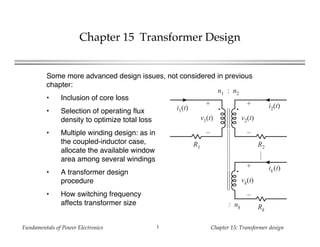
  • 1. Fundamentals of Power Electronics Chapter 15: Transformer design1 Chapter 15 Transformer Design Some more advanced design issues, not considered in previous chapter: • Inclusion of core loss • Selection of operating flux density to optimize total loss • Multiple winding design: as in the coupled-inductor case, allocate the available window area among several windings • A transformer design procedure • How switching frequency affects transformer size n1 : n2 : nk R1 R2 Rk + v1(t) – + v2(t) – + vk(t) – i1(t) i2(t) ik(t)
  • 2. Fundamentals of Power Electronics Chapter 15: Transformer design2 Chapter 15 Transformer Design 15.1 Transformer design: Basic constraints 15.2 A step-by-step transformer design procedure 15.3 Examples 15.4 AC inductor design 15.5 Summary
  • 3. Fundamentals of Power Electronics Chapter 15: Transformer design3 15.1 Transformer Design: Basic Constraints Core loss Typical value of for ferrite materials: 2.6 or 2.7 B is the peak value of the ac component of B(t), i.e., the peak ac flux density So increasing B causes core loss to increase rapidly This is the first constraint Pfe = K fe(∆B)β Ac lm
  • 4. Fundamentals of Power Electronics Chapter 15: Transformer design4 Flux density Constraint #2 Flux density B(t) is related to the applied winding voltage according to Faraday’s Law. Denote the volt- seconds applied to the primary winding during the positive portion of v1(t) as 1: λ1 = v1(t)dt t1 t2 This causes the flux to change from its negative peak to its positive peak. From Faraday’s law, the peak value of the ac component of flux density is To attain a given flux density, the primary turns should be chosen according to area λ1 v1(t) t1 t2 t ∆B = λ1 2n1Ac n1 = λ1 2∆BAc
  • 5. Fundamentals of Power Electronics Chapter 15: Transformer design5 Copper loss Constraint #3 • Allocate window area between windings in optimum manner, as described in previous section • Total copper loss is then equal to Pcu = ρ(MLT)n1 2 Itot 2 WAKu Itot = nj n1 IjΣj = 1 k with Eliminate n1, using result of previous slide: Note that copper loss decreases rapidly as B is increased Pcu = ρλ1 2 Itot 2 4Ku (MLT) WAAc 2 1 ∆B 2
  • 6. Fundamentals of Power Electronics Chapter 15: Transformer design6 Total power loss 4. Ptot = Pcu + Pfe Ptot = Pfe + Pcu There is a value of B that minimizes the total power loss Pcu = ρλ1 2 Itot 2 4Ku (MLT) WAAc 2 1 ∆B 2 Pfe = K fe(∆B)β Ac lm ∆B Power loss Ptot CopperlossPcu CorelossP fe Optimum ∆B
  • 7. Fundamentals of Power Electronics Chapter 15: Transformer design7 5. Find optimum flux density B Ptot = Pfe + Pcu Given that Then, at the B that minimizes Ptot, we can write Note: optimum does not necessarily occur where Pfe = Pcu. Rather, it occurs where dPtot d(∆B) = dPfe d(∆B) + dPcu d(∆B) = 0 dPfe d(∆B) = – dPcu d(∆B)
  • 8. Fundamentals of Power Electronics Chapter 15: Transformer design8 Take derivatives of core and copper loss Now, substitute into and solve for B: Optimum B for a given core and application Pcu = ρλ1 2 Itot 2 4Ku (MLT) WAAc 2 1 ∆B 2 Pfe = K fe(∆B)β Ac lm dPfe d(∆B) = βK fe(∆B) β – 1 Aclm dPcu d(∆B) = – 2 ρλ1 2 Itot 2 4Ku (MLT) WAAc 2 (∆B)– 3 dPfe d(∆B) = – dPcu d(∆B) ∆B = ρλ1 2 Itot 2 2Ku (MLT) WAAc 3 lm 1 βK fe 1 β + 2
  • 9. Fundamentals of Power Electronics Chapter 15: Transformer design9 Total loss Substitute optimum B into expressions for Pcu and Pfe. The total loss is: Rearrange as follows: Left side: terms depend on core geometry Right side: terms depend on specifications of the application Ptot = AclmK fe 2 β + 2 ρλ1 2 Itot 2 4Ku (MLT) WAAc 2 β β + 2 β 2 – β β + 2 + β 2 2 β + 2 WA Ac 2(β – 1)/β (MLT)lm 2/β β 2 – β β + 2 + β 2 2 β + 2 – β + 2 β = ρλ1 2 Itot 2 K fe 2/β 4Ku Ptot β + 2 /β
  • 10. Fundamentals of Power Electronics Chapter 15: Transformer design10 The core geometrical constant Kgfe Define Design procedure: select a core that satisfies Appendix D lists the values of Kgfe for common ferrite cores Kgfe is similar to the Kg geometrical constant used in Chapter 14: • Kg is used when Bmax is specified • Kgfe is used when B is to be chosen to minimize total loss Kgfe = WA Ac 2(β – 1)/β (MLT)lm 2/β β 2 – β β + 2 + β 2 2 β + 2 – β + 2 β Kgfe ≥ ρλ1 2 Itot 2 K fe 2/β 4Ku Ptot β + 2 /β
  • 11. Fundamentals of Power Electronics Chapter 15: Transformer design11 15.2 Step-by-step transformer design procedure The following quantities are specified, using the units noted: Wire effective resistivity ( -cm) Total rms winding current, ref to pri Itot (A) Desired turns ratios n2/n1, n3/n1, etc. Applied pri volt-sec 1 (V-sec) Allowed total power dissipation Ptot (W) Winding fill factor Ku Core loss exponent Core loss coefficient Kfe (W/cm3T ) Other quantities and their dimensions: Core cross-sectional area Ac (cm2) Core window area WA (cm2) Mean length per turn MLT (cm) Magnetic path length le (cm) Wire areas Aw1, … (cm2) Peak ac flux density B (T)
  • 12. Fundamentals of Power Electronics Chapter 15: Transformer design12 Procedure 1. Determine core size Select a core from Appendix D that satisfies this inequality. It may be possible to reduce the core size by choosing a core material that has lower loss, i.e., lower Kfe. Kgfe ≥ ρλ1 2 Itot 2 K fe 2/β 4Ku Ptot β + 2 /β 108
  • 13. Fundamentals of Power Electronics Chapter 15: Transformer design13 2. Evaluate peak ac flux density At this point, one should check whether the saturation flux density is exceeded. If the core operates with a flux dc bias Bdc, then B + Bdc should be less than the saturation flux density Bsat. If the core will saturate, then there are two choices: • Specify B using the Kg method of Chapter 14, or • Choose a core material having greater core loss, then repeat steps 1 and 2 ∆B = 108 ρλ1 2 Itot 2 2Ku (MLT) WAAc 3 lm 1 βK fe 1 β + 2
  • 14. Fundamentals of Power Electronics Chapter 15: Transformer design14 3. and 4. Evaluate turns Primary turns: Choose secondary turns according to desired turns ratios: n2 = n1 n2 n1 n3 = n1 n3 n1 n1 = λ1 2∆BAc 104
  • 15. Fundamentals of Power Electronics Chapter 15: Transformer design15 5. and 6. Choose wire sizes α1 = n1I1 n1Itot α2 = n2I2 n1Itot αk = nkIk n1Itot Fraction of window area assigned to each winding: Choose wire sizes according to: Aw1 ≤ α1KuWA n1 Aw2 ≤ α2KuWA n2
  • 16. Fundamentals of Power Electronics Chapter 15: Transformer design16 Check: computed transformer model iM, pk = λ1 2LM R1 = ρn1(MLT) Aw1 R2 = ρn2(MLT) Aw2 Predicted magnetizing inductance, referred to primary: Peak magnetizing current: Predicted winding resistances: n1 : n2 : nk R1 R2 Rk i1(t) i2(t) ik(t) LM iM(t) LM = µn1 2 Ac lm
  • 17. Fundamentals of Power Electronics Chapter 15: Transformer design17 15.4.1 Example 1: Single-output isolated Cuk converter 100 W fs = 200 kHz D = 0.5 n = 5 Ku = 0.5 Allow Ptot = 0.25 W Use a ferrite pot core, with Magnetics Inc. P material. Loss parameters at 200 kHz are Kfe = 24.7 = 2.6 + – + V 5 V – Vg 25 V n : 1 I 20 A Ig 4 A + v2(t) – – v1(t) + i1(t) i2(t) – vC2(t) ++ vC1(t) –
  • 18. Fundamentals of Power Electronics Chapter 15: Transformer design18 Waveforms v1(t) i1(t) i2(t) DTs Area λ1VC1 – nVC2 D'Ts I/n – Ig I – nIg Applied primary volt- seconds: λ1 = DTsVc1 = (0.5) (5 µsec ) (25 V) = 62.5 V–µsec Applied primary rms current: I1 = D I n 2 + D' Ig 2 = 4 A Applied secondary rms current: I2 = nI1 = 20 A Total rms winding current: Itot = I1 + 1 n I2 = 8 A
  • 19. Fundamentals of Power Electronics Chapter 15: Transformer design19 Choose core size Kgfe ≥ (1.724⋅10– 6 )(62.5⋅10– 6 )2 (8)2 (24.7) 2/2.6 4 (0.5) (0.25) 4.6/2.6 108 = 0.00295 Pot core data of Appendix D lists 2213 pot core with Kgfe = 0.0049 Next smaller pot core is not large enough.
  • 20. Fundamentals of Power Electronics Chapter 15: Transformer design20 Evaluate peak ac flux density This is much less than the saturation flux density of approximately 0.35 T. Values of B in the vicinity of 0.1 T are typical for ferrite designs that operate at frequencies in the vicinity of 100 kHz. ∆B = 108 (1.724⋅10– 6 )(62.5⋅10– 6 )2 (8)2 2 (0.5) (4.42) (0.297)(0.635)3 (3.15) 1 (2.6)(24.7) 1/4.6 = 0.0858 Tesla
  • 21. Fundamentals of Power Electronics Chapter 15: Transformer design21 Evaluate turns n1 = 104 (62.5⋅10– 6 ) 2(0.0858)(0.635) = 5.74 turns n2 = n1 n = 1.15 turns In practice, we might select n1 = 5 and n2 = 1 This would lead to a slightly higher flux density and slightly higher loss.
  • 22. Fundamentals of Power Electronics Chapter 15: Transformer design22 Determine wire sizes Fraction of window area allocated to each winding: α1 = 4 A 8 A = 0.5 α2 = 1 5 20 A 8 A = 0.5 (Since, in this example, the ratio of winding rms currents is equal to the turns ratio, equal areas are allocated to each winding) Wire areas: Aw1 = (0.5)(0.5)(0.297) (5) = 14.8⋅10– 3 cm2 Aw2 = (0.5)(0.5)(0.297) (1) = 74.2⋅10– 3 cm2 From wire table, Appendix D: AWG #16 AWG #9
  • 23. Fundamentals of Power Electronics Chapter 15: Transformer design23 Wire sizes: discussion Primary 5 turns #16 AWG Secondary 1 turn #9 AWG • Very large conductors! • One turn of #9 AWG is not a practical solution Some alternatives • Use foil windings • Use Litz wire or parallel strands of wire
  • 24. Fundamentals of Power Electronics Chapter 15: Transformer design24 Effect of switching frequency on transformer size for this P-material Cuk converter example 0 0.02 0.04 0.06 0.08 0.1 Switching frequency Bmax,Tesla Potcoresize 4226 3622 2616 2213 1811 1811 2213 2616 25 kHz 50 kHz 100 kHz 200 kHz 250 kHz 400 kHz 500 kHz 1000 kHz • As switching frequency is increased from 25 kHz to 250 kHz, core size is dramatically reduced • As switching frequency is increased from 400 kHz to 1 MHz, core size increases
  • 25. Fundamentals of Power Electronics Chapter 15: Transformer design25 15.3.2 Example 2 Multiple-Output Full-Bridge Buck Converter Switching frequency 150 kHz Transformer frequency 75 kHz Turns ratio 110:5:15 Optimize transformer at D = 0.75 : n2 + v1(t) – + – D1 Q1 D2Q2 D3 Q3 D4Q4 i1(t) + 5 V – D5 D6 I5V 100 Ai2a(t) + 15 V – D7 D8 i3a(t) n1 : : n2 : n3 : n3 i2b(t) i2b(t) I15V 15 A T1 Vg 160 V
  • 26. Fundamentals of Power Electronics Chapter 15: Transformer design26 Other transformer design details Use Magnetics, Inc. ferrite P material. Loss parameters at 75 kHz: Kfe = 7.6 W/T cm3 = 2.6 Use E-E core shape Assume fill factor of Ku = 0.25 (reduced fill factor accounts for added insulation required in multiple-output off-line application) Allow transformer total power loss of Ptot = 4 W (approximately 0.5% of total output power) Use copper wire, with = 1.724·10–6 -cm
  • 27. Fundamentals of Power Electronics Chapter 15: Transformer design27 Applied transformer waveforms t i2a(t) 0 i3a(t) 0 DTs Ts 2Ts Ts +DTs i1(t) 0 v1(t) 0 0 Vg – Vg Area λ1 = Vg DTs n2 n1 I5V + n3 n1 I15V – n2 n1 I5V + n3 n1 I15V I5V 0.5I5V I15V 0.5I15V 0 : n2 + v1(t) – D3 D4 i1(t) D5 D6 i2a(t) D7 D8 i3a(t) n1 : : n2 : n3 : n3 i2b(t) i2b(t) T1
  • 28. Fundamentals of Power Electronics Chapter 15: Transformer design28 Applied primary volt-seconds v1(t) 0 0 Vg – Vg Area λ1 = Vg DTs λ1 = DTsVg = (0.75) (6.67 µsec ) (160 V) = 800 V–µsec
  • 29. Fundamentals of Power Electronics Chapter 15: Transformer design29 Applied primary rms current i1(t) 0 n2 n1 I5V + n3 n1 I15V – n2 n1 I5V + n3 n1 I15V I1 = n2 n1 I5V + n3 n1 I15V D = 5.7 A
  • 30. Fundamentals of Power Electronics Chapter 15: Transformer design30 Applied rms current, secondary windings t i2a(t) 0 i3a(t) 0 DTs Ts 2TsTs+DTs I5V 0.5I5V I15V 0.5I15V 0 I3 = 1 2 I15V 1 + D = 9.9 A I2 = 1 2 I5V 1 + D = 66.1 A
  • 31. Fundamentals of Power Electronics Chapter 15: Transformer design31 Itot RMS currents, summed over all windings and referred to primary Itot = nj n1 IjΣall 5 windings = I1 + 2 n2 n1 I2 + 2 n3 n1 I3 = 5.7 A + 5 110 66.1 A + 15 110 9.9 A = 14.4 A
  • 32. Fundamentals of Power Electronics Chapter 15: Transformer design32 Select core size Kgfe ≥ (1.724⋅10– 6 )(800⋅10– 6 )2 (14.4)2 (7.6) 2/2.6 4 (0.25) (4) 4.6/2.6 108 = 0.00937 A From Appendix D
  • 33. Fundamentals of Power Electronics Chapter 15: Transformer design33 Evaluate ac flux density B Bmax = 108 ρλ1 2 Itot 2 2Ku (MLT) WAAc 3 lm 1 βK fe 1 β + 2 Eq. (15.20): Plug in values: This is less than the saturation flux density of approximately 0.35 T ∆B = 108 (1.724⋅10– 6 )(800⋅10– 6 )2 (14.4)2 2(0.25) (8.5) (1.1)(1.27)3 (7.7) 1 (2.6)(7.6) 1/4.6 = 0.23 Tesla
  • 34. Fundamentals of Power Electronics Chapter 15: Transformer design34 Evaluate turns Choose n1 according to Eq. (15.21): n1 = 104 (800⋅10– 6 ) 2(0.23)(1.27) = 13.7 turns Choose secondary turns according to desired turns ratios: n2 = 5 110 n1 = 0.62 turns n3 = 15 110 n1 = 1.87 turns Rounding the number of turns To obtain desired turns ratio of 110:5:15 we might round the actual turns to 22:1:3 Increased n1 would lead to • Less core loss • More copper loss • Increased total loss n1 = λ1 2∆BAc 104
  • 35. Fundamentals of Power Electronics Chapter 15: Transformer design35 Loss calculation with rounded turns With n1 = 22, the flux density will be reduced to The resulting losses will be Pfe = (7.6)(0.143)2.6 (1.27)(7.7) = 0.47 W Pcu = (1.724⋅10– 6 )(800⋅10– 6 )2 (14.4)2 4 (0.25) (8.5) (1.1)(1.27)2 1 (0.143)2 108 = 5.4 W Ptot = Pfe + Pcu = 5.9 W Which exceeds design goal of 4 W by 50%. So use next larger core size: EE50. ∆B = (800⋅10– 6 ) 2(22)(1.27) 104 = 0.143 Tesla
  • 36. Fundamentals of Power Electronics Chapter 15: Transformer design36 Calculations with EE50 Repeat previous calculations for EE50 core size. Results: B = 0.14 T, n1 = 12, Ptot = 2.3 W Again round n1 to 22. Then B = 0.08 T, Pcu = 3.89 W, Pfe = 0.23 W, Ptot = 4.12 W Which is close enough to 4 W.
  • 37. Fundamentals of Power Electronics Chapter 15: Transformer design37 Wire sizes for EE50 design Aw1 = α1KuWA n1 = (0.396)(0.25)(1.78) (22) = 8.0⋅10– 3 cm2 ⇒ AWG #19 Aw2 = α2KuWA n2 = (0.209)(0.25)(1.78) (1) = 93.0⋅10– 3 cm2 ⇒ AWG #8 Aw3 = α3KuWA n3 = (0.094)(0.25)(1.78) (3) = 13.9⋅10– 3 cm2 ⇒ AWG #16 α1 = I1 Itot = 5.7 14.4 = 0.396 α2 = n2I2 n1Itot = 5 110 66.1 14.4 = 0.209 α3 = n3I3 n1Itot = 15 110 9.9 14.4 = 0.094 Window allocations Wire gauges Might actually use foil or Litz wire for secondary windings
  • 38. Fundamentals of Power Electronics Chapter 15: Transformer design38 Discussion: Transformer design • Process is iterative because of round-off of physical number of turns and, to a lesser extent, other quantities • Effect of proximity loss – Not included in design process yet – Requires additional iterations • Can modify procedure as follows: – After a design has been calculated, determine number of layers in each winding and then compute proximity loss – Alter effective resistivity of wire to compensate: define eff = Pcu/Pdc where Pcu is the total copper loss (including proximity effects) and Pdc is the copper loss predicted by the dc resistance. – Apply transformer design procedure using this effective wire resistivity, and compute proximity loss in the resulting design. Further iterations may be necessary if the specifications are not met.
  • 39. Fundamentals of Power Electronics Chapter 15: Transformer design39 15.4 AC Inductor Design + v(t) – L i(t) Core Window area WA Core mean length per turn (MLT) Wire resistivity ρ Fill factor Ku Air gap lg n turns Core area Ac Area λ v(t) t1 t2 t i(t) Design a single-winding inductor, having an air gap, accounting for core loss (note that the previous design procedure of this chapter did not employ an air gap, and inductance was not a specification)
  • 40. Fundamentals of Power Electronics Chapter 15: Transformer design40 Outline of key equations L = µ0Acn2 lg ∆B = λ 2nAc Obtain specified inductance: Relationship between applied volt-seconds and peak ac flux density: Pcu = ρn2(MLT) KuWA I2 Copper loss (using dc resistance): ∆B = ρλ2 I2 2Ku (MLT) WAAc 3 lm 1 βK fe 1 β + 2 Total loss is minimized when Kgfe ≥ ρλ2 I2 K fe 2/β 2Ku Ptot β + 2 /β Must select core that satisfies See Section 15.4.2 for step-by-step design equations