SlideShare una empresa de Scribd logo
1 de 38
Descargar para leer sin conexión
Experiment No :-1
Objective:- Implementation of HALF ADDER, FULL ADDER using basic logic gates.
Theory:- An adder is a digital circuit that performs addition of numbers. The half adder adds two
binary digits called as augend and addend and produces two outputs as sum and carry; XOR is
applied to both inputs to produce sum and AND gate is applied to both inputs to produce carry. The
full adder adds 3 one bit numbers, where two can be referred to as operands and one can be
referred to as bit carried in. And produces 2-bit output, and these can be referred to as output carry
and sum.
Half Adder
By using half adder, you can design simple addition with the help of logic gates.
Half Adder
0+0 = 0
0+1 = 1
1+0 = 1
1+1 = 10
Half Adder Truth Table
Now it has been cleared that 1-bit adder can be easily implemented with the help of the XOR Gate
for the output ‘SUM’ and an AND Gate for the ‘Carry’. When we need to add, two 8-bit bytes
together, we can be done with the help of a full-adder logic. The half-adder is useful when you want
to add one binary digit quantities. A way to develop a two-binary digit adders would be to make a
truth table and reduce it. When you want to make a three binary digit adder, do it again. When you
decide to make a four digit adder, do it again. The circuits would be fast, but development time is
slow.
Half Adder Logic Circuit
VHDL Code For half Adder
entity ha is
Port (a: in STD_LOGIC;
b : in STD_LOGIC;
sha : out STD_LOGIC;
cha : out STD_LOGIC);
end ha;
architecture Behavioral of ha is
begin
sha <= a xor b ;
cha <= a and b ;
end Behavioral
Full Adder
The output carry is designated as C-OUT and the normal output is designated as S.
Full Adder Truth Table:
With the truth-table, the full adder logic can be implemented. You can see that the output S is an
XOR between the input A and the half-adder, SUM output with B and C-IN inputs. We take C-OUT
will only be true if any of the two inputs out of the three are HIGH.
So, we can implement a full adder circuit with the help of two half adder circuits. At first, half adder
will be used to add A and B to produce a partial Sum and a second half adder logic can be used to
add C-IN to the Sum produced by the first half adder to get the final S output.
The implementation of larger logic diagrams is possible with the above full adder logic a simpler
symbol is mostly used to represent the operation. Given below is a simpler schematic representation
of a one-bit full adder.
Full Adder Design Using Half Adders
With this type of symbol, we can add two bits together, taking a carry from the next lower order of magnitude,
and sending a carry to the next higher order of magnitude. In a computer, for a multi-bit operation, each bit
must be represented by a full adder and must be added simultaneously. Thus, to add two 8-bit numbers, you
will need 8 full adders which can be formed by cascading two of the 4-bit blocks.
Full-Adder is of two Half-Adders, the Full-Adder is the actual block that we use to create the
arithmetic circuits.
VHDL Coding for Full Adder
entity full_add is
Port ( a : in STD_LOGIC;
b : in STD_LOGIC;
cin : in STD_LOGIC;
sum : out STD_LOGIC;
cout : out STD_LOGIC);
end full_add;
architecture Behavioral of full_add is
component ha is
Port ( a : in STD_LOGIC;
b : in STD_LOGIC;
sha : out STD_LOGIC;
cha : out STD_LOGIC);
end component;
signal s_s,c1,c2: STD_LOGIC ;
begin
HA1:ha port map(a,b,s_s,c1);
HA2:ha port map (s_s,cin,sum,c2);
cout<=c1 or c2 ;
end Behavioral;
Experiment no:- 2
Objective:- Implementing Binary -to -Gray, Gray -to -Binary code conversions.
Theory:-
In computers, we need to convert binary to gray and gray to binary. The conversion of this can be
done by using two rules namely binary to gray conversion and gray to binary conversion. In the first
conversion, the MSB of the gray code is constantly equivalent to the MSB of the binary code. Additional
bits of the gray code’s output can get using EX-OR logic gate concept to the binary codes at that
present index as well as the earlier index. Here MSB is nothing but the most significant bit. In the first
conversion, the MSB of the binary code is constantly equivalent to the MSB of the particular binary
code. Additional bits of the binary code’s output can get using EX-OR logic gate concept by verifying
gray codes at that present index
Binary to Gray Code Converter
The conversion of binary to gray code can be done by using a logic circuit. The gray code is a non-
weighted code because there is no particular weight is assigned for the position of the bit. A n-bit code
can be attained by reproducing a n-1 bit code on an axis subsequent to the rows of 2n-1
, as well as
placing the most significant bit of 0 over the axis with the most significant bit of 1 beneath the axis. The
step by step gray code generation is shown below.
This method uses an Ex-OR gate to perform among the binary bits.
Binary to Gray Code Converter Table
Decimal
Number Binary Code Gray Code
0 0000 0000
1 0001 0001
2 0010 0011
3 0011 0010
4 0100 0110
5 0101 0111
6 0110 0101
7 0111 0100
8 1000 1100
9 1001 1101
10 1010 1111
11 1011 1110
12 1100 1010
13 1101 1011
14 1110 1001
Gray to Binary Code Converter
This gray to binary conversion method also uses the working concept of EX-OR logic gate among the
bits of gray as well as binary bits. The following example with step by step procedure may help to know
the conversion concept of gray code to binary code.
To change gray to binary code, take down the MSB digit of the gray code number, as the primary digit
or the MSB of the gray code is similar to the binary digit.
To get the next straight binary bit, it uses the XOR operation among the primary bit or MSB bit of binary
to the next bit of the gray code.
Similarly, to get the third straight binary bit, it uses the XOR operation among the second bit or MSB
bit of binary to the third MSD bit of the gray code and so on.
Gray to Binary Code Converter Table
Decimal Number Gray Code Binary Code
0 0000 0000
1 0001 0001
2 0010 0011
3 0010 0011
4 0110 0100
5 0111 0101
6 0101 0110
7 0100 0111
8 1100 1000
9 1101 1001
10 1111 1010
11 1110 1011
12 1010 1100
Experiment :- 3
Objective:- Implementing 3-8 line DECODER.
Theory :-
3 Line to 8 Line Decoder
This decoder circuit gives 8 logic outputs for 3 inputs and has a enable pin. The circuit
is designed with AND and NAND logic gates. It takes 3 binary inputs and activates one
of the eight outputs. 3 to 8 line decoder circuit is also called as binary to an octal decoder.
3 to 8 Line Decoder Block Diagram
The decoder circuit works only when the Enable pin (E) is high. S0, S1 and S2 are three different
inputs and D0, D1, D2, D3. D4. D5. D6. D7 are the eight outputs.
Circuit Diagram
3 to 8 Decoder Circuit
3 to 8 Line Decoder Truth Table
The below table gives the truth table of 3 to 8 line decoder.
S0 S1 S2 E D0 D1 D2 D3 D4 D5 D6 D7
x x x 0 0 0 0 0 0 0 0 0
0 0 0 1 0 0 0 0 0 0 0 1
0 0 1 1 0 0 0 0 0 0 1 0
0 1 0 1 0 0 0 0 0 1 0 0
0 1 1 1 0 0 0 0 1 0 0 0
1 0 0 1 0 0 0 1 0 0 0 0
1 0 1 1 0 0 1 0 0 0 0 0
1 1 0 1 0 1 0 0 0 0 0 0
1 1 1 1 1 0 0 0 0 0 0 0
Experiment no:- 4
Objective : implementing 4*1 and 8*1 Multiplexer.
THEORY: A multiplexer is a device that performs multiplexing i.e. it selects one of many
analog or digital input signals and forwards the selected input into a single line. A multiplexer
of 2n
inputs has n select lines, which are used to select which input line to be sent to the
output.
A Boolean equation for 8×1 Multiplexer is
Z = A’.B’.C’ + A’.B’.C + A’.B.C’ + A’.B.C + A.B’.C’ + A.B’.C + A.B.C’ + A.B.C
TRUTH TABLE:
S0 S1 S2 Z
0 0 0 A
0 0 1 B
0 1 0 C
0 1 1 D
1 0 0 E
1 0 1 F
1 1 0 G
1 1 1 H
SCHEMATIC DIAGRAM:
A Boolean equation for 4×1 Multiplexer is
Q = abA + abB + abC + abD
Truth table:-
Waveform of 4*1 MUX
Waveform of 8*1 MUX
RESULT: The output waveform of 8×1 and 4*1 Multiplexer is verified.
Experiment :- 5
Objective :- Verify the excitation tables of various FLIP-FLOPS.
To realize and implement
1. Set-Reset (SR) latch using NOR gates (active high circuit).
2. SR, JK, D, and T Flip-Flops using IC’s and breadboard.
Components Required:
 Mini Digital Training and Digital Electronic Sets.
 IC 7404, IC 7408, IC 7411, IC 7474, IC 7476.
Theory:
Logic circuits for digital systems are either combinational or sequential. The output of
combinational circuits depends only on the current inputs. In contrast, sequential
circuit depends not only on the current value of the input but also upon the internal
state of the circuit. Basic building blocks (memory elements) of a sequential circuit are
the flip-flops (FFs). The FFs change their output state depending upon inputs at
certain interval of time synchronized with some clock pulse applied to it. Usually any
flip-flop has normal inputs, present state Q(t) as circuit inputs and two outputs; next
state Q(t+1) and its complementary value; Q`. We shall discuss most widely used
latches that are listed below.
 SR Flip-Flop
 D Flip-Flop
 JK Flip-Flop
 T Flip-Flop
SR Flip-Flop
SR flip-flop operates with only positive clock transitions or negative clock transitions.
Whereas, SR latch operates with enable signal. The circuit diagram of SR flip-flop is
shown in the following figure.
This circuit has two inputs S & R and two outputs Q(t) & Q(t)’. The operation of SR flipflop
is similar to SR Latch. But, this flip-flop affects the outputs only when positive transition
of the clock signal is applied instead of active enable.
The following table shows the state table of SR flip-flop.
S R Q(t + 1)
0 0 Q(t)
0 1 0
1 0 1
1 1 -
Here, Q(t) & Q(t + 1) are present state & next state respectively. So, SR flip-flop can be
used for one of these three functions such as Hold, Reset & Set based on the input
conditions, when positive transition of clock signal is applied. The following table shows
the characteristic table of SR flip-flop.
Present Inputs Present State Next State
S R Q(t) Q(t + 1)
0 0 0 0
0 0 1 1
0 1 0 0
0 1 1 0
1 0 0 1
1 0 1 1
1 1 0 x
1 1 1 x
By using three variable K-Map, we can get the simplified expression for next state, Q(t
+ 1). The three variable K-Map for next state, Q(t + 1) is shown in the following figure.
The maximum possible groupings of adjacent ones are already shown in the figure.
Therefore, the simplified expression for next state Q(t + 1) is
[Math Processing Error]Q(t+1)=S+R′Q(t)
D Flip-Flop
D flip-flop operates with only positive clock transitions or negative clock transitions.
Whereas, D latch operates with enable signal. That means, the output of D flip-flop is
insensitive to the changes in the input, D except for active transition of the clock signal.
The circuit diagram of D flip-flop is shown in the following figure.
This circuit has single input D and two outputs Q(t) & Q(t)’. The operation of D flip-flop
is similar to D Latch. But, this flip-flop affects the outputs only when positive transition
of the clock signal is applied instead of active enable.
The following table shows the state table of D flip-flop.
D Q(t + 1)
0 0
0 1
Therefore, D flip-flop always Hold the information, which is available on data input, D of
earlier positive transition of clock signal. From the above state table, we can directly
write the next state equation as
Q(t + 1) = D
Next state of D flip-flop is always equal to data input, D for every positive transition of
the clock signal. Hence, D flip-flops can be used in registers, shift registers and some
of the counters.
JK Flip-Flop
JK flip-flop is the modified version of SR flip-flop. It operates with only positive clock
transitions or negative clock transitions. The circuit diagram of JK flip-flop is shown in
the following figure.
This circuit has two inputs J & K and two outputs Q(t) & Q(t)’. The operation of JK flip-
flop is similar to SR flip-flop. Here, we considered the inputs of SR flip-flop as S = J
Q(t)’ and R = KQ(t) in order to utilize the modified SR flip-flop for 4 combinations of
inputs.
The following table shows the state table of JK flip-flop.
J K Q(t + 1)
0 0 Q(t)
0 1 0
1 0 1
1 1 Q(t)'
Here, Q(t) & Q(t + 1) are present state & next state respectively. So, JK flip-flop can be
used for one of these four functions such as Hold, Reset, Set & Complement of present
state based on the input conditions, when positive transition of clock signal is applied.
The following table shows the characteristic table of JK flip-flop.
Present Inputs Present State Next State
J K Q(t) Q(t+1)
0 0 0 0
0 0 1 1
0 1 0 0
0 1 1 0
1 0 0 1
1 0 1 1
1 1 0 1
1 1 1 0
By using three variable K-Map, we can get the simplified expression for next state, Q(t
+ 1). Three variable K-Map for next state, Q(t + 1) is shown in the following figure.
The maximum possible groupings of adjacent ones are already shown in the figure.
Therefore, the simplified expression for next state Q(t+1) is
[Math Processing Error]Q(t+1)=JQ(t)′+K′Q(t)
T Flip-Flop
T flip-flop is the simplified version of JK flip-flop. It is obtained by connecting the same
input ‘T’ to both inputs of JK flip-flop. It operates with only positive clock transitions or
negative clock transitions. The circuit diagram of T flip-flop is shown in the following
figure.
This circuit has single input T and two outputs Q(t) & Q(t)’. The operation of T flip-flop
is same as that of JK flip-flop. Here, we considered the inputs of JK flip-flop as J =
T and K = T in order to utilize the modified JK flip-flop for 2 combinations of inputs. So,
we eliminated the other two combinations of J & K, for which those two values are
complement to each other in T flip-flop.
The following table shows the state table of T flip-flop.
D Q(t + 1)
0 Q(t)
1 Q(t)’
Here, Q(t) & Q(t + 1) are present state & next state respectively. So, T flip-flop can be
used for one of these two functions such as Hold, & Complement of present state based
on the input conditions, when positive transition of clock signal is applied. The following
table shows the characteristic table of T flip-flop.
Inputs Present State Next State
T Q(t) Q(t + 1)
0 0 0
0 1 1
1 0 1
1 1 0
From the above characteristic table, we can directly write the next state equation as
[Math Processing Error]Q(t+1)=T′Q(t)+TQ(t)′
[Math Processing Error]⇒Q(t+1)=T⊕Q(t)
The output of T flip-flop always toggles for every positive transition of the clock signal,
when input T remains at logic High (1). Hence, T flip-flop can be used in counters.
Output:-
we implemented various flip-flops by providing the cross coupling between NOR
gates. Similarly, you can implement these flip-flops by using NAND gates
Experiment no:- 6
Objective: - Design the 8- bit arithmetic logic unit
Theory: -
The designing 8 bit ALU using Verilog programming language. It includes
writing, compiling and simulating Verilog code in ModelSim on a Windows platform.
ModelSim is an easy-to-use, versatile VHDL/SystemVerilog/Verilog/SystemC simulator by
Mentor Graphics. It supports behavioural, register-transfer-level and gate-level modelling.
Fig. 2: ALU architecture for designing 8 bit ALU
Fig. 3: Create Project window
First, install ModelSim on a Windows PC.
1. Start ModelSim from desktop; you will see ModelSim 10.4 dialogue window.
2. Create a project by clicking Jumpstart on the Welcome screen.
3. A Create Project window pops up. Select a suitable name for your project.
Set Project Location to C:/Documents and Settings/Nitesh/Desktop/Final_ALU_Testing (in our case)
and leave the rest as default, followed by clicking OK.
3. An Add items to the Project window pops up (Fig. 4).
4. On this window, select Create New File option.
5. A Create Project File window pops up. Select an appropriate file name (say,Top_ALU) for the file
you want to add; choose Verilog as Add file as type and Top Level as Folder (Fig. 5).
6. On the workspace section of the main window (Fig. 6), double-click on the file you have just
created (Top_ALU.v in our case).
7. Type in your Verilog code (Top_ALU.v) for an 8-bit ALU in the new window.
8. Save your code from File menu.
9. Now, add relevant files as per the architecture, which includes arithmetic, logic, shift and MUX
units. Add new files to Top_ALU project by right-clicking Top_ALU.v file. Select Add to Project ->
New File… options as shown in Fig. 7.
Fig. 6: Workspace window
Give File Name Top Arithmetic and follow the steps from five through nine as mentioned above.
Similarly, add Top_Logic, Top_Shift and Top_Mux files into the project and enter respective Verilog
codes in these files.
The final workspace window is shown in Fig. 8.
Fig. 7: Adding new filesFig. 8: Workspace section
Fig. 9: Compilation windownknk
Fig. 10: Library tab
Fig. 11: Add wave to the project
Compiling/debugging project files
1. Select Compile->Compile All options.
2. The compilation result is shown on the main window. A green tick is shown against each file name,
which means there are no errors in the project (Fig. 9).
Simulating the ALU design
1. Click on Library menu from the main window and then click on the plus (+) sign next to the work
library. You should see the name Top_ALU code that we have just compiled (Fig. 10).
2. Double-click on ALU to load the file. This should open a third tab sim in the main window.
3. Go to Add ->To Wave-> All items in region options (Fig. 11).
4. Select the signals that you want to monitor for simulation purposes. Select these as shown in Fig. 12.
5. Provide values manually to monitor the simulation of the eight-bit ALU design.
Fig. 12:
Selecting the signalsFig. 13: Monitoring signals
Fig. 14: Simulation
window Fig. 15:
Wave window
Right-click on the selected signals and click on Force.
After providing values to selected signals, we are now ready to simulate our design by clicking Run in
the simulation window.
RESULT:- The ALU design is verified from this output waveform.
Experiment no :-7
Objective :- Design the control unit of a computer using either hardwiring or
microprogramming based on its register transfer language description.
Theory: -
Control Unit is the part of the computer’s central processing unit (CPU), which
directs the operation of the processor. It was included as part of the Von Neumann
Architecture by John von Neumann. It is the responsibility of the Control Unit to tell the
computer’s memory, arithmetic/logic unit and input and output devices how to respond
to the instructions that have been sent to the processor. It fetches internal instructions
of the programs from the main memory to the processor instruction register, and based
on this register contents, the control unit generates a control signal that supervises the
execution of these instructions.
A control unit works by receiving input information to which it converts into control
signals, which are then sent to the central processor. The computer’s processor then
tells the attached hardware what operations to perform. The functions that a control unit
performs are dependent on the type of CPU because the architecture of CPU varies
from manufacturer to manufacturer. Examples of devices that require a CU are:
 Control Processing Units(CPUs)
 Graphics Processing Units(GPUs)

Types of Control Unit –
There are two types of control units: Hardwired control unit and Microprogrammable
control unit.
1. Hardwired Control Unit –
In the Hardwired control unit, the control signals that are important for instruction
execution control are generated by specially designed hardware logical circuits, in
which we can not modify the signal generation method without physical change of
the circuit structure. The operation code of an instruction contains the basic data
for control signal generation. In the instruction decoder, the operation code is
decoded. The instruction decoder constitutes a set of many decoders that decode
different fields of the instruction opcode.
As a result, few output lines going out from the instruction decoder obtains active
signal values. These output lines are connected to the inputs of the matrix that
generates control signals for executive units of the computer. This matrix
implements logical combinations of the decoded signals from the instruction
opcode with the outputs from the matrix that generates signals representing
consecutive control unit states and with signals coming from the outside of the
processor, e.g. interrupt signals. The matrices are built in a similar way as a
programmable logic arrays.
Control signals for an instruction execution have to be generated not in a single
time point but during the entire time interval that corresponds to the instruction
execution cycle. Following the structure of this cycle, the suitable sequence of
internal states is organized in the control unit.
A number of signals generated by the control signal generator matrix are sent
back to inputs of the next control state generator matrix. This matrix combines
these signals with the timing signals, which are generated by the timing unit
based on the rectangular patterns usually supplied by the quartz generator. When
a new instruction arrives at the control unit, the control units is in the initial state of
new instruction fetching. Instruction decoding allows the control unit enters the
first state relating execution of the new instruction, which lasts as long as the
timing signals and other input signals as flags and state information of the
computer remain unaltered. A change of any of the earlier mentioned signals
stimulates the change of the control unit state.
This causes that a new respective input is generated for the control signal
generator matrix. When an external signal appears, (e.g. an interrupt) the control
unit takes entry into a next control state that is the state concerned with the
reaction to this external signal (e.g. interrupt processing). The values of flags and
state variables of the computer are used to select suitable states for the
instruction execution cycle.
The last states in the cycle are control states that commence fetching the next
instruction of the program: sending the program counter content to the main
memory address buffer register and next, reading the instruction word to the
instruction register of computer. When the ongoing instruction is the stop
instruction that ends program execution, the control unit enters an operating
system state, in which it waits for a next user directive.
2. Microprogrammable control unit –
The fundamental difference between these unit structures and the structure of the
hardwired control unit is the existence of the control store that is used for storing
words containing encoded control signals mandatory for instruction execution.
In microprogrammed control units, subsequent instruction words are fetched into
the instruction register in a normal way. However, the operation code of each
instruction is not directly decoded to enable immediate control signal generation
but it comprises the initial address of a microprogram contained in the control
store.
 With a single-level control store:
In this, the instruction opcode from the instruction register is sent to the
control store address register. Based on this address, the first
microinstruction of a microprogram that interprets execution of this instruction
is read to the microinstruction register. This microinstruction contains in its
operation part encoded control signals, normally as few bit fields. In a set
microinstruction field decoders, the fields are decoded. The microinstruction
also contains the address of the next microinstruction of the given instruction
microprogram and a control field used to control activities of the
microinstruction address generator.
 The last mentioned field decides the addressing mode (addressing operation) to
be applied to the address embedded in the ongoing microinstruction. In
microinstructions along with conditional addressing mode, this address is refined
by using the processor condition flags that represent the status of computations
in the current program. The last microinstruction in the instruction of the given
microprogram is the microinstruction that fetches the next instruction from the
main memory to the instruction register.
 With a two-level control store:
In this, in a control unit with a two-level control store, besides the control
memory for microinstructions, a nano-instruction memory is included. In such a
control unit, microinstructions do not contain encoded control signals. The
operation part of microinstructions contains the address of the word in the nano-
instruction memory, which contains encoded control signals. The nano-
instruction memory contains all combinations of control signals that appear in
microprograms that interpret the complete instruction set of a given computer,
written once in the form of nano-instructions.
In this way, unnecessary storing of the same operation parts of microinstructions is
avoided. In this case, microinstruction word can be much shorter than with the single
level control store. It gives a much smaller size in bits of the microinstruction memory
and, as a result, a much smaller size of the entire control memory. The microinstruction
memory contains the control for selection of consecutive microinstructions, while those
control signals are generated at the basis of nano-instructions. In nano-instructions,
control signals are frequently encoded using 1 bit/ 1 signal method that eliminates
decoding.
Result :- The control unit design is verified from this output signal..
Experiment no: - 8
Objective: - Implement a simple instruction set computer with a control unit and a data path.
Theory: -
We will examine the MIPS implementation for a simple subset that shows most aspects of implementation.
The instructions considered are:
 The memory-reference instructions load word (lw) and store word (sw)
 The arithmetic-logical instructions add, sub, and, or, and slt
 The instructions branch equal (beq) and jump (j) to be considered in the end.
This subset does not include all the integer instructions (for example, shift, multiply, and divide are missing),
nor does it include any floating-point instructions. However, the key principles used in creating a datapath and
designing the control will be illustrated. The implementation of the remaining instructions is similar
When we look at the instruction cycle of any processor, it should involve the following operations:
 Fetch instruction from memory
 Decode the instruction
 Fetch the operands
 Execute the instruction
 Write the result
We shall look at each of these steps in detail for the subset of instructionsFor every instruction, the first two
steps of instruction fetch and decode are identical:
 Send the program counter (PC) to the program memory that contains the code and fetch the instruction
 Read one or two registers, using the register specifier fields in the instruction. For the load word instruction, we
need to read only one register, but most other instructions require that we read two registers. Since MIPS uses a
fixed length format with the register specifiers in the same place, the registers can be read, irrespective of the
instruction.
After these two steps, the actions required to complete the instruction depend on the type of instruction. For
each of the three instruction classes, arithmetic/logical, memory-reference and branches, the actions are mostly
the same. Even across different instruction classes there are some similarities. A memory-reference instruction
will need to access the memory. For a load instruction, a memory read has to be performed. For a store
instruction, a memory write has to be performed. An arithmetic/logical instruction must write the data from the
ALU back into a register. A load instruction also has to write the data fetched form memory to a register. Lastly,
for a branch instruction, we may need to change the next instruction address based on the comparison. If the
condition of comparison fails, the PC should be incremented by 4 to get the address of the next instruction. If
the condition is true, the new address will have to updated in the PC.
However, wherever we have two possibilities of inputs, we cannot join wires together.
We have to use multiplexers as indicated below in Figure 8.3.
We also need to include the necessary control signals. Figure 8.4 below shows the datapath, as well as the
control lines for the major functional units. The control unit takes in the instruction as an input and determines
how to set the control lines for the functional units and two of the multiplexors. The third multiplexor, which
determines whether PC + 4 or the branch destination address is written into the PC, is set based on the zero
output of the ALU, which is used to perform the comparison of a branch on equal instruction. The regularity and
simplicity of the MIPS instruction set means that a simple decoding process can be used to determine how to set
the control lines.
Just to give a brief section on the logic design basics, all of you know that information is encoded in binary as
low voltage = 0, high voltage = 1 and there is one wire per bit. Multi-bit data are encoded on multi-wire buses.
The combinational elements operate on data and the output is a function of input. In the case of state (sequential)
elements, they store information and the output is a function of both inputs and the stored data, that is, the
previous inputs. Examples of combinational elements are AND-gates, XOR-gates, etc. An example of a
sequential element is a register that stores data in a circuit. It uses a clock signal to determine when to update the
stored value and is edge-triggered.
Now, we shall discuss the implementation of the datapath. The datapath comprises of the elements that process
data and addresses in the CPU – Registers, ALUs, mux’s, memories, etc. We will build a MIPS datapath
incrementally. We shall construct the basic model and keep refining it.
The portion of the CPU that carries out the instruction fetch operation is given in Figure 8.5.
As mentioned earlier, The PC is used to address the instruction memory to fetch the instruction. At the same
time, the PC value is also fed to the adder unit and added with 4, so that PC+4, which is the address of the next
instruction in MIPS is written into the PC, thus making it ready for the next instruction fetch.
The next step is instruction decoding and operand fetch. In the case of MIPS, decoding is done and at the same
time, the register file is read. The processor’s 32 general-purpose registers are stored in a structure called a
register file. A register file is a collection of registers in which any register can be read or written by specifying
the number of the register in the file.
The R-format instructions have three register operands and we will need to read two data words from the
register file and write one data word into the register file for each instruction. For each data word to be read from
the registers, we need an input to the register file that specifies the register number to be read and an output from
the register file that will carry the value that has been read from the registers. To write a data word, we will need
two inputs- one to specify the register number to be written and one to supply the data to be written into the
register. The 5-bit register specifiers indicate one of the 32 registers to be used.
The register file always outputs the contents of whatever register numbers are on the Read register inputs.
Writes, however, are controlled by the write control signal, which must be asserted for a write to occur at the
clock edge. Thus, we need a total of four inputs (three for register numbers and one for data) and two outputs
(both for data), as shown in Figure 8.6. The register number inputs are 5 bits wide to specify one of 32 registers,
whereas the data input and two data output buses are each 32 bits wide.
After the two register contents are read, the next step is to pass on these two data to the ALU and perform the
required operation, as decided by the control unit and the control signals. It might be an add, subtract or any
other type of operation, depending on the opcode. Thus the ALU takes two 32-bit inputs and produces a 32-bit
result, as well as a 1-bit signal if the result is 0. The control signals will be discussed in the next module. For
now, we wil assume that the appropriate control signals are somehow generated.
The same arithmetic or logical operation with an immediate operand and a register operand, uses the I-type of
instruction format. Here, Rs forms one of the source operands and the immediate component forms the second
operand. These two will have to be fed to the ALU. Before that, the 16-bit immediate operand is sign extended
to form a 32-bit operand. This sign extension is done by the sign extension unit.
We shall next consider the MIPS load word and store word instructions, which have the general form lw
$t1,offset_value($t2) or sw $t1,offset_value ($t2). These instructions compute a memory address by adding the
base register, which is $t2, to the 16-bit signed offset field contained in the instruction. If the instruction is a
store, the value to be stored must also be read from the register file where it resides in $t1. If the instruction is a
load, the value read from memory must be written into the register file in the specified register, which is $t1.
Thus, we will need both the register file and the ALU. In addition, the sign extension unit will sign extend the
16-bit offset field in the instruction to a 32-bit signed value. The next operation for the load and store operations
is the data memory access. The data memory unit has to be read for a load instruction and the data memory must
be written for store instructions; hence, it has both read and write control signals, an address input, as well as an
input for the data to be written into memory. Figure 8.7 above illustrates all this.
The branch on equal instruction has three operands, two registers that are compared for equality, and a 16-bit
offset used to compute the branch target address, relative to the branch instruction address. Its form is beq $t1,
$t2, offset. To implement this instruction, we must compute the branch target address by adding the sign-
extended offset field of the instruction to the PC. The instruction set architecture specifies that the base for the
branch address calculation is the address of the instruction following the branch. Since we have already computed
PC + 4, the address of the next instruction, in the instruction fetch datapath, it is easy to use this value as the base
for computing the branch target address. Also, since the word boundaries have the 2 LSBs as zeros and branch
target addresses must start at word boundaries, the offset field is shifted left 2 bits. In addition to computing the
branch target address, we must also determine whether the next instruction is the instruction that follows
sequentially or the instruction at the branch target address. This depends on the condition being evaluated. When
the condition is true (i.e., the operands are equal), the branch target address becomes the new PC, and we say
that the branch is taken. If the operands are not equal, the incremented PC should replace the current PC (just as
for any other normal instruction); in this case, we say that the branch is not taken.
Thus, the branch datapath must do two operations: compute the branch target address and compare the register
contents. This is illustrated in Figure 8.8. To compute the branch target address, the branch datapath includes a
sign extension unit and an adder. To perform the compare, we need to use the register file to supply the two
register operands. Since the ALU provides an output signal that indicates whether the result was 0, we can send
the two register operands to the ALU with the control set to do a subtract. If the Zero signal out of the ALU unit
is asserted, we know that the two values are equal. Although the Zero output always signals if the result is 0, we
will be using it only to implement the equal test of branches. Later, we will show exactly how to connect the
control signals of the ALU for use in the datapath.
Now, that we have examined the datapath components needed for the individual instruction classes, we can
combine them into a single datapath and add the control to complete the implementation. The combined datapath
is shown Figure 8.9 below.
The simplest datapath might attempt to execute all instructions in one clock cycle. This means that no datapath
resource can be used more than once per instruction, so any element needed more than once must be duplicated.
We therefore need a memory for instructions separate from one for data. Although some of the functional units
will need to be duplicated, many of the elements can be shared by different instruction flows. To share a datapath
element between two different instruction classes, we may need to allow multiple connections to the input of an
element, using a multiplexor and control signal to select among the multiple inputs. While adding multiplexors,
we should note that though the operations of arithmetic/logical ( R-type) instructions and the memory related
instructions datapath are quite similar, there are certain key differences.
 The R-type instructions use two register operands coming from the register file. The memory instructions also
use the ALU to do the address calculation, but the second input is the sign-extended 16-bit offset field from the
instruction.
 The value stored into a destination register comes from the ALU for an R-type instruction, whereas, the data
comes from memory for a load.
To create a datapath with a common register file and ALU, we must support two different sources for the
second ALU input, as well as two different sources for the data stored into the register file. Thus, one multiplexor
needs to be placed at the ALU input and another at the data input to the register file, as shown in Figure 8.10.
Result :- Implementation of simple instruction set is verified from this output working.
Experiment no: - 9
Objective: - Design the data path of a computer from its register transfer language
description.
Register Transfer Language, RTL, (sometimes called register transfer notation) is a
powerful high level method of describing the architecture of a circuit. VHDL code and
schematics are often created from RTL. RTL describes the transfer of data from register
to register, known as microinstructions or microoperations. Transfers may be
conditional. Each microinstruction completes in one clock cycle. A typical RTL statement
will look like the following:
A v B --> R1 <-- R2;
This is read as "if signal A or signal B is true then register R2 is transferred to register
R1". The first part, A v B, is a logical expression that must be true for the transfer to take
place. The --> symbol separates the logical expression from the microinstruction. It is
the if-then part of the statement. If there isn't a logical expression, --> isn't in the
statement and the microinstruction will always take place. To the right of --> is the
microinstruction. It describes a transfer of data and operations on the data from register
to register. The above RTL statement is equivalent to the following schematic:
For RTL we will use the following symbols:
<-- Register transfer
[ ] Word index
< > Bit index
n..m Index range
--> If-then
:= Definition
# Concatenation
: Parallel separator
; Sequential separator
@ Replication
{ } Operation modifier
( ) Operation or value grouping
= != < <= > >= Comparison operators
+ - * / Arithmetic operators
^ v ' xor Logical operators
RTL examples
Example 1
K1 --> R0 <-- R1 : K1' ^ K2 --> R0 <-- R2 ;
Special Math Processor
Processor Diagram
Processor State (using RTL)
RA<15..0>: Register A (input to multiplier and adder)
RB<15..0>: Register B (input to multiplier and adder)
RC<15..0>: Register C (output from multiplier or adder)
PC<7..0>: Program Counter (Address of next instruction)
RI<7..0>: Register I (memory index register)
IR<11..0>: Instruction Register
Reset: Reset signal
op<3..0> := IR<11..8>: Operation code field
M[255..0]<15..0>: Main memory 255 words.
Processor Schematic
Computer Organization And Architecture lab manual

Más contenido relacionado

La actualidad más candente

Binary parallel adder
Binary parallel adderBinary parallel adder
Binary parallel adderanu surya
 
Programmable Logic Array(PLA) & Programmable Array Logic(PAL)
Programmable Logic Array(PLA) & Programmable Array Logic(PAL)Programmable Logic Array(PLA) & Programmable Array Logic(PAL)
Programmable Logic Array(PLA) & Programmable Array Logic(PAL)Revathi Subramaniam
 
Multiplexer and DeMultiplexer
Multiplexer and DeMultiplexerMultiplexer and DeMultiplexer
Multiplexer and DeMultiplexerEstiak Khan
 
Logic gates ppt
Logic gates pptLogic gates ppt
Logic gates pptparassini
 
Register transfer language
Register transfer languageRegister transfer language
Register transfer languageSanjeev Patel
 
Octal to binary encoder
Octal to binary encoderOctal to binary encoder
Octal to binary encoderAjay844
 
SOP POS, Minterm and Maxterm
SOP POS, Minterm and MaxtermSOP POS, Minterm and Maxterm
SOP POS, Minterm and MaxtermSelf-employed
 
decoder and encoder
 decoder and encoder decoder and encoder
decoder and encoderUnsa Shakir
 
basic logic gates
 basic logic gates basic logic gates
basic logic gatesvishal gupta
 
Floating point arithmetic operations (1)
Floating point arithmetic operations (1)Floating point arithmetic operations (1)
Floating point arithmetic operations (1)cs19club
 
Pipeline hazard
Pipeline hazardPipeline hazard
Pipeline hazardAJAL A J
 
1.ripple carry adder, full adder implementation using half adder.
1.ripple carry adder, full adder implementation using half adder.1.ripple carry adder, full adder implementation using half adder.
1.ripple carry adder, full adder implementation using half adder.MdFazleRabbi18
 
What is Adder-Half and Full Adder
What is Adder-Half and Full AdderWhat is Adder-Half and Full Adder
What is Adder-Half and Full AdderAdeel Rasheed
 
bus and memory tranfer (computer organaization)
bus and memory tranfer (computer organaization)bus and memory tranfer (computer organaization)
bus and memory tranfer (computer organaization)Siddhi Viradiya
 
Decoders-Digital Electronics
Decoders-Digital ElectronicsDecoders-Digital Electronics
Decoders-Digital ElectronicsPaurav Shah
 

La actualidad más candente (20)

Ripple Carry Adder
Ripple Carry AdderRipple Carry Adder
Ripple Carry Adder
 
Binary parallel adder
Binary parallel adderBinary parallel adder
Binary parallel adder
 
Programmable Logic Array(PLA) & Programmable Array Logic(PAL)
Programmable Logic Array(PLA) & Programmable Array Logic(PAL)Programmable Logic Array(PLA) & Programmable Array Logic(PAL)
Programmable Logic Array(PLA) & Programmable Array Logic(PAL)
 
Multiplexer and DeMultiplexer
Multiplexer and DeMultiplexerMultiplexer and DeMultiplexer
Multiplexer and DeMultiplexer
 
Logic gates ppt
Logic gates pptLogic gates ppt
Logic gates ppt
 
Subtractor (1)
Subtractor (1)Subtractor (1)
Subtractor (1)
 
Register transfer language
Register transfer languageRegister transfer language
Register transfer language
 
Octal to binary encoder
Octal to binary encoderOctal to binary encoder
Octal to binary encoder
 
SOP POS, Minterm and Maxterm
SOP POS, Minterm and MaxtermSOP POS, Minterm and Maxterm
SOP POS, Minterm and Maxterm
 
MULTIPLEXER
MULTIPLEXERMULTIPLEXER
MULTIPLEXER
 
decoder and encoder
 decoder and encoder decoder and encoder
decoder and encoder
 
basic logic gates
 basic logic gates basic logic gates
basic logic gates
 
Floating point arithmetic operations (1)
Floating point arithmetic operations (1)Floating point arithmetic operations (1)
Floating point arithmetic operations (1)
 
Pipeline hazard
Pipeline hazardPipeline hazard
Pipeline hazard
 
1.ripple carry adder, full adder implementation using half adder.
1.ripple carry adder, full adder implementation using half adder.1.ripple carry adder, full adder implementation using half adder.
1.ripple carry adder, full adder implementation using half adder.
 
What is Adder-Half and Full Adder
What is Adder-Half and Full AdderWhat is Adder-Half and Full Adder
What is Adder-Half and Full Adder
 
Logic gates
Logic gatesLogic gates
Logic gates
 
Binary parallel adder
Binary parallel adderBinary parallel adder
Binary parallel adder
 
bus and memory tranfer (computer organaization)
bus and memory tranfer (computer organaization)bus and memory tranfer (computer organaization)
bus and memory tranfer (computer organaization)
 
Decoders-Digital Electronics
Decoders-Digital ElectronicsDecoders-Digital Electronics
Decoders-Digital Electronics
 

Similar a Computer Organization And Architecture lab manual

Digital electronics lab
Digital electronics labDigital electronics lab
Digital electronics labswatymanoja
 
Combinational and sequential logic
Combinational and sequential logicCombinational and sequential logic
Combinational and sequential logicDeepak John
 
COMPUTER ORGANIZATION NOTES Unit 6
COMPUTER ORGANIZATION NOTES Unit 6COMPUTER ORGANIZATION NOTES Unit 6
COMPUTER ORGANIZATION NOTES Unit 6Dr.MAYA NAYAK
 
CHAPTER 6: Function of Combination Logic From Flyod ( Digital Logic Design )
CHAPTER 6: Function of Combination Logic From Flyod ( Digital Logic Design ) CHAPTER 6: Function of Combination Logic From Flyod ( Digital Logic Design )
CHAPTER 6: Function of Combination Logic From Flyod ( Digital Logic Design ) Sefat Ahammed Shovo
 
Logic System Design KTU Chapter-4.ppt
Logic System Design KTU Chapter-4.pptLogic System Design KTU Chapter-4.ppt
Logic System Design KTU Chapter-4.pptAlbin562191
 
Unit 3 Arithmetic building blocks and memory Design (1).pdf
Unit 3 Arithmetic building blocks and  memory Design (1).pdfUnit 3 Arithmetic building blocks and  memory Design (1).pdf
Unit 3 Arithmetic building blocks and memory Design (1).pdfShreyasMahesh
 
Lec 05 - Combinational Logic
Lec 05 - Combinational LogicLec 05 - Combinational Logic
Lec 05 - Combinational LogicVajira Thambawita
 
UNIT - II.pptx
UNIT - II.pptxUNIT - II.pptx
UNIT - II.pptxamudhak10
 

Similar a Computer Organization And Architecture lab manual (20)

Lect 1 unit 2.pdf
Lect 1 unit 2.pdfLect 1 unit 2.pdf
Lect 1 unit 2.pdf
 
Chapter-04.pdf
Chapter-04.pdfChapter-04.pdf
Chapter-04.pdf
 
B sc3 unit 4 combi..lckt
B sc3 unit 4 combi..lcktB sc3 unit 4 combi..lckt
B sc3 unit 4 combi..lckt
 
Digital Logic Design
Digital Logic Design Digital Logic Design
Digital Logic Design
 
Chapter 4: Combinational Logic
Chapter 4: Combinational LogicChapter 4: Combinational Logic
Chapter 4: Combinational Logic
 
Digital electronics lab
Digital electronics labDigital electronics lab
Digital electronics lab
 
Combinational and sequential logic
Combinational and sequential logicCombinational and sequential logic
Combinational and sequential logic
 
Combinational circuits
Combinational circuitsCombinational circuits
Combinational circuits
 
Logic gates
Logic gatesLogic gates
Logic gates
 
COMPUTER ORGANIZATION NOTES Unit 6
COMPUTER ORGANIZATION NOTES Unit 6COMPUTER ORGANIZATION NOTES Unit 6
COMPUTER ORGANIZATION NOTES Unit 6
 
STLD-Combinational logic design
STLD-Combinational  logic design STLD-Combinational  logic design
STLD-Combinational logic design
 
CHAPTER 6: Function of Combination Logic From Flyod ( Digital Logic Design )
CHAPTER 6: Function of Combination Logic From Flyod ( Digital Logic Design ) CHAPTER 6: Function of Combination Logic From Flyod ( Digital Logic Design )
CHAPTER 6: Function of Combination Logic From Flyod ( Digital Logic Design )
 
Digital Logic circuit
Digital Logic circuitDigital Logic circuit
Digital Logic circuit
 
Deld lab manual
Deld lab manualDeld lab manual
Deld lab manual
 
Logic System Design KTU Chapter-4.ppt
Logic System Design KTU Chapter-4.pptLogic System Design KTU Chapter-4.ppt
Logic System Design KTU Chapter-4.ppt
 
Lecturer mid.ppt
Lecturer mid.pptLecturer mid.ppt
Lecturer mid.ppt
 
Unit 3 Arithmetic building blocks and memory Design (1).pdf
Unit 3 Arithmetic building blocks and  memory Design (1).pdfUnit 3 Arithmetic building blocks and  memory Design (1).pdf
Unit 3 Arithmetic building blocks and memory Design (1).pdf
 
Lec 05 - Combinational Logic
Lec 05 - Combinational LogicLec 05 - Combinational Logic
Lec 05 - Combinational Logic
 
UNIT - II.pptx
UNIT - II.pptxUNIT - II.pptx
UNIT - II.pptx
 
Chapter5 dek3133
Chapter5 dek3133Chapter5 dek3133
Chapter5 dek3133
 

Más de Nitesh Dubey

MLApproachToProgramming.ppt
MLApproachToProgramming.pptMLApproachToProgramming.ppt
MLApproachToProgramming.pptNitesh Dubey
 
seminar topic of holography.ppt
seminar topic of holography.pptseminar topic of holography.ppt
seminar topic of holography.pptNitesh Dubey
 
Compiler design.pdf
Compiler design.pdfCompiler design.pdf
Compiler design.pdfNitesh Dubey
 
Online shopping ppt
Online shopping pptOnline shopping ppt
Online shopping pptNitesh Dubey
 
Python lab manual all the experiments are available
Python lab manual all the experiments are availablePython lab manual all the experiments are available
Python lab manual all the experiments are availableNitesh Dubey
 
Web Technology Lab files with practical
Web Technology Lab  files with practicalWeb Technology Lab  files with practical
Web Technology Lab files with practicalNitesh Dubey
 
Theory of automata and formal language lab manual
Theory of automata and formal language lab manualTheory of automata and formal language lab manual
Theory of automata and formal language lab manualNitesh Dubey
 
Software engineering practical
Software engineering practicalSoftware engineering practical
Software engineering practicalNitesh Dubey
 
Principal of programming language lab files
Principal of programming language lab files Principal of programming language lab files
Principal of programming language lab files Nitesh Dubey
 
database management system lab files
database management system lab filesdatabase management system lab files
database management system lab filesNitesh Dubey
 
design and analysis of algorithm Lab files
design and analysis of algorithm Lab filesdesign and analysis of algorithm Lab files
design and analysis of algorithm Lab filesNitesh Dubey
 
industrial training report on Ethical hacking
industrial training report on Ethical hackingindustrial training report on Ethical hacking
industrial training report on Ethical hackingNitesh Dubey
 
Project synopsis on face recognition in e attendance
Project synopsis on face recognition in e attendanceProject synopsis on face recognition in e attendance
Project synopsis on face recognition in e attendanceNitesh Dubey
 
Hrms industrial training report
Hrms industrial training reportHrms industrial training report
Hrms industrial training reportNitesh Dubey
 
Industrial training report on core java
Industrial training report on core java Industrial training report on core java
Industrial training report on core java Nitesh Dubey
 
SEWAGE TREATMENT PLANT mini project report
SEWAGE TREATMENT PLANT mini project reportSEWAGE TREATMENT PLANT mini project report
SEWAGE TREATMENT PLANT mini project reportNitesh Dubey
 
synopsis report on BIOMETRIC ONLINE VOTING SYSTEM
synopsis report on BIOMETRIC ONLINE VOTING SYSTEMsynopsis report on BIOMETRIC ONLINE VOTING SYSTEM
synopsis report on BIOMETRIC ONLINE VOTING SYSTEMNitesh Dubey
 
artificial intelligence ppt
artificial intelligence pptartificial intelligence ppt
artificial intelligence pptNitesh Dubey
 
object oriented Programming ppt
object oriented Programming pptobject oriented Programming ppt
object oriented Programming pptNitesh Dubey
 

Más de Nitesh Dubey (20)

HTML Presentation
HTML  PresentationHTML  Presentation
HTML Presentation
 
MLApproachToProgramming.ppt
MLApproachToProgramming.pptMLApproachToProgramming.ppt
MLApproachToProgramming.ppt
 
seminar topic of holography.ppt
seminar topic of holography.pptseminar topic of holography.ppt
seminar topic of holography.ppt
 
Compiler design.pdf
Compiler design.pdfCompiler design.pdf
Compiler design.pdf
 
Online shopping ppt
Online shopping pptOnline shopping ppt
Online shopping ppt
 
Python lab manual all the experiments are available
Python lab manual all the experiments are availablePython lab manual all the experiments are available
Python lab manual all the experiments are available
 
Web Technology Lab files with practical
Web Technology Lab  files with practicalWeb Technology Lab  files with practical
Web Technology Lab files with practical
 
Theory of automata and formal language lab manual
Theory of automata and formal language lab manualTheory of automata and formal language lab manual
Theory of automata and formal language lab manual
 
Software engineering practical
Software engineering practicalSoftware engineering practical
Software engineering practical
 
Principal of programming language lab files
Principal of programming language lab files Principal of programming language lab files
Principal of programming language lab files
 
database management system lab files
database management system lab filesdatabase management system lab files
database management system lab files
 
design and analysis of algorithm Lab files
design and analysis of algorithm Lab filesdesign and analysis of algorithm Lab files
design and analysis of algorithm Lab files
 
industrial training report on Ethical hacking
industrial training report on Ethical hackingindustrial training report on Ethical hacking
industrial training report on Ethical hacking
 
Project synopsis on face recognition in e attendance
Project synopsis on face recognition in e attendanceProject synopsis on face recognition in e attendance
Project synopsis on face recognition in e attendance
 
Hrms industrial training report
Hrms industrial training reportHrms industrial training report
Hrms industrial training report
 
Industrial training report on core java
Industrial training report on core java Industrial training report on core java
Industrial training report on core java
 
SEWAGE TREATMENT PLANT mini project report
SEWAGE TREATMENT PLANT mini project reportSEWAGE TREATMENT PLANT mini project report
SEWAGE TREATMENT PLANT mini project report
 
synopsis report on BIOMETRIC ONLINE VOTING SYSTEM
synopsis report on BIOMETRIC ONLINE VOTING SYSTEMsynopsis report on BIOMETRIC ONLINE VOTING SYSTEM
synopsis report on BIOMETRIC ONLINE VOTING SYSTEM
 
artificial intelligence ppt
artificial intelligence pptartificial intelligence ppt
artificial intelligence ppt
 
object oriented Programming ppt
object oriented Programming pptobject oriented Programming ppt
object oriented Programming ppt
 

Último

Forming section troubleshooting checklist for improving wire life (1).ppt
Forming section troubleshooting checklist for improving wire life (1).pptForming section troubleshooting checklist for improving wire life (1).ppt
Forming section troubleshooting checklist for improving wire life (1).pptNoman khan
 
Robotics Group 10 (Control Schemes) cse.pdf
Robotics Group 10  (Control Schemes) cse.pdfRobotics Group 10  (Control Schemes) cse.pdf
Robotics Group 10 (Control Schemes) cse.pdfsahilsajad201
 
The Satellite applications in telecommunication
The Satellite applications in telecommunicationThe Satellite applications in telecommunication
The Satellite applications in telecommunicationnovrain7111
 
Immutable Image-Based Operating Systems - EW2024.pdf
Immutable Image-Based Operating Systems - EW2024.pdfImmutable Image-Based Operating Systems - EW2024.pdf
Immutable Image-Based Operating Systems - EW2024.pdfDrew Moseley
 
Secure Key Crypto - Tech Paper JET Tech Labs
Secure Key Crypto - Tech Paper JET Tech LabsSecure Key Crypto - Tech Paper JET Tech Labs
Secure Key Crypto - Tech Paper JET Tech Labsamber724300
 
22CYT12 & Chemistry for Computer Systems_Unit-II-Corrosion & its Control Meth...
22CYT12 & Chemistry for Computer Systems_Unit-II-Corrosion & its Control Meth...22CYT12 & Chemistry for Computer Systems_Unit-II-Corrosion & its Control Meth...
22CYT12 & Chemistry for Computer Systems_Unit-II-Corrosion & its Control Meth...KrishnaveniKrishnara1
 
AntColonyOptimizationManetNetworkAODV.pptx
AntColonyOptimizationManetNetworkAODV.pptxAntColonyOptimizationManetNetworkAODV.pptx
AntColonyOptimizationManetNetworkAODV.pptxLina Kadam
 
CME 397 - SURFACE ENGINEERING - UNIT 1 FULL NOTES
CME 397 - SURFACE ENGINEERING - UNIT 1 FULL NOTESCME 397 - SURFACE ENGINEERING - UNIT 1 FULL NOTES
CME 397 - SURFACE ENGINEERING - UNIT 1 FULL NOTESkarthi keyan
 
Module-1-(Building Acoustics) Noise Control (Unit-3). pdf
Module-1-(Building Acoustics) Noise Control (Unit-3). pdfModule-1-(Building Acoustics) Noise Control (Unit-3). pdf
Module-1-(Building Acoustics) Noise Control (Unit-3). pdfManish Kumar
 
Novel 3D-Printed Soft Linear and Bending Actuators
Novel 3D-Printed Soft Linear and Bending ActuatorsNovel 3D-Printed Soft Linear and Bending Actuators
Novel 3D-Printed Soft Linear and Bending ActuatorsResearcher Researcher
 
US Department of Education FAFSA Week of Action
US Department of Education FAFSA Week of ActionUS Department of Education FAFSA Week of Action
US Department of Education FAFSA Week of ActionMebane Rash
 
Mine Environment II Lab_MI10448MI__________.pptx
Mine Environment II Lab_MI10448MI__________.pptxMine Environment II Lab_MI10448MI__________.pptx
Mine Environment II Lab_MI10448MI__________.pptxRomil Mishra
 
Robotics-Asimov's Laws, Mechanical Subsystems, Robot Kinematics, Robot Dynami...
Robotics-Asimov's Laws, Mechanical Subsystems, Robot Kinematics, Robot Dynami...Robotics-Asimov's Laws, Mechanical Subsystems, Robot Kinematics, Robot Dynami...
Robotics-Asimov's Laws, Mechanical Subsystems, Robot Kinematics, Robot Dynami...Sumanth A
 
Input Output Management in Operating System
Input Output Management in Operating SystemInput Output Management in Operating System
Input Output Management in Operating SystemRashmi Bhat
 
Analysis and Evaluation of Dal Lake Biomass for Conversion to Fuel/Green fert...
Analysis and Evaluation of Dal Lake Biomass for Conversion to Fuel/Green fert...Analysis and Evaluation of Dal Lake Biomass for Conversion to Fuel/Green fert...
Analysis and Evaluation of Dal Lake Biomass for Conversion to Fuel/Green fert...arifengg7
 
Virtual memory management in Operating System
Virtual memory management in Operating SystemVirtual memory management in Operating System
Virtual memory management in Operating SystemRashmi Bhat
 
Katarzyna Lipka-Sidor - BIM School Course
Katarzyna Lipka-Sidor - BIM School CourseKatarzyna Lipka-Sidor - BIM School Course
Katarzyna Lipka-Sidor - BIM School Coursebim.edu.pl
 
"Exploring the Essential Functions and Design Considerations of Spillways in ...
"Exploring the Essential Functions and Design Considerations of Spillways in ..."Exploring the Essential Functions and Design Considerations of Spillways in ...
"Exploring the Essential Functions and Design Considerations of Spillways in ...Erbil Polytechnic University
 
70 POWER PLANT IAE V2500 technical training
70 POWER PLANT IAE V2500 technical training70 POWER PLANT IAE V2500 technical training
70 POWER PLANT IAE V2500 technical trainingGladiatorsKasper
 

Último (20)

Forming section troubleshooting checklist for improving wire life (1).ppt
Forming section troubleshooting checklist for improving wire life (1).pptForming section troubleshooting checklist for improving wire life (1).ppt
Forming section troubleshooting checklist for improving wire life (1).ppt
 
Robotics Group 10 (Control Schemes) cse.pdf
Robotics Group 10  (Control Schemes) cse.pdfRobotics Group 10  (Control Schemes) cse.pdf
Robotics Group 10 (Control Schemes) cse.pdf
 
The Satellite applications in telecommunication
The Satellite applications in telecommunicationThe Satellite applications in telecommunication
The Satellite applications in telecommunication
 
Immutable Image-Based Operating Systems - EW2024.pdf
Immutable Image-Based Operating Systems - EW2024.pdfImmutable Image-Based Operating Systems - EW2024.pdf
Immutable Image-Based Operating Systems - EW2024.pdf
 
Secure Key Crypto - Tech Paper JET Tech Labs
Secure Key Crypto - Tech Paper JET Tech LabsSecure Key Crypto - Tech Paper JET Tech Labs
Secure Key Crypto - Tech Paper JET Tech Labs
 
22CYT12 & Chemistry for Computer Systems_Unit-II-Corrosion & its Control Meth...
22CYT12 & Chemistry for Computer Systems_Unit-II-Corrosion & its Control Meth...22CYT12 & Chemistry for Computer Systems_Unit-II-Corrosion & its Control Meth...
22CYT12 & Chemistry for Computer Systems_Unit-II-Corrosion & its Control Meth...
 
AntColonyOptimizationManetNetworkAODV.pptx
AntColonyOptimizationManetNetworkAODV.pptxAntColonyOptimizationManetNetworkAODV.pptx
AntColonyOptimizationManetNetworkAODV.pptx
 
CME 397 - SURFACE ENGINEERING - UNIT 1 FULL NOTES
CME 397 - SURFACE ENGINEERING - UNIT 1 FULL NOTESCME 397 - SURFACE ENGINEERING - UNIT 1 FULL NOTES
CME 397 - SURFACE ENGINEERING - UNIT 1 FULL NOTES
 
Module-1-(Building Acoustics) Noise Control (Unit-3). pdf
Module-1-(Building Acoustics) Noise Control (Unit-3). pdfModule-1-(Building Acoustics) Noise Control (Unit-3). pdf
Module-1-(Building Acoustics) Noise Control (Unit-3). pdf
 
Novel 3D-Printed Soft Linear and Bending Actuators
Novel 3D-Printed Soft Linear and Bending ActuatorsNovel 3D-Printed Soft Linear and Bending Actuators
Novel 3D-Printed Soft Linear and Bending Actuators
 
US Department of Education FAFSA Week of Action
US Department of Education FAFSA Week of ActionUS Department of Education FAFSA Week of Action
US Department of Education FAFSA Week of Action
 
Mine Environment II Lab_MI10448MI__________.pptx
Mine Environment II Lab_MI10448MI__________.pptxMine Environment II Lab_MI10448MI__________.pptx
Mine Environment II Lab_MI10448MI__________.pptx
 
Robotics-Asimov's Laws, Mechanical Subsystems, Robot Kinematics, Robot Dynami...
Robotics-Asimov's Laws, Mechanical Subsystems, Robot Kinematics, Robot Dynami...Robotics-Asimov's Laws, Mechanical Subsystems, Robot Kinematics, Robot Dynami...
Robotics-Asimov's Laws, Mechanical Subsystems, Robot Kinematics, Robot Dynami...
 
Input Output Management in Operating System
Input Output Management in Operating SystemInput Output Management in Operating System
Input Output Management in Operating System
 
Analysis and Evaluation of Dal Lake Biomass for Conversion to Fuel/Green fert...
Analysis and Evaluation of Dal Lake Biomass for Conversion to Fuel/Green fert...Analysis and Evaluation of Dal Lake Biomass for Conversion to Fuel/Green fert...
Analysis and Evaluation of Dal Lake Biomass for Conversion to Fuel/Green fert...
 
Virtual memory management in Operating System
Virtual memory management in Operating SystemVirtual memory management in Operating System
Virtual memory management in Operating System
 
Katarzyna Lipka-Sidor - BIM School Course
Katarzyna Lipka-Sidor - BIM School CourseKatarzyna Lipka-Sidor - BIM School Course
Katarzyna Lipka-Sidor - BIM School Course
 
"Exploring the Essential Functions and Design Considerations of Spillways in ...
"Exploring the Essential Functions and Design Considerations of Spillways in ..."Exploring the Essential Functions and Design Considerations of Spillways in ...
"Exploring the Essential Functions and Design Considerations of Spillways in ...
 
Versatile Engineering Construction Firms
Versatile Engineering Construction FirmsVersatile Engineering Construction Firms
Versatile Engineering Construction Firms
 
70 POWER PLANT IAE V2500 technical training
70 POWER PLANT IAE V2500 technical training70 POWER PLANT IAE V2500 technical training
70 POWER PLANT IAE V2500 technical training
 

Computer Organization And Architecture lab manual

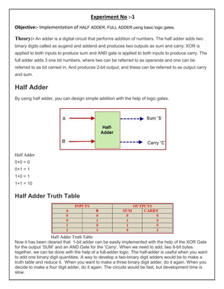
  • 1. Experiment No :-1 Objective:- Implementation of HALF ADDER, FULL ADDER using basic logic gates. Theory:- An adder is a digital circuit that performs addition of numbers. The half adder adds two binary digits called as augend and addend and produces two outputs as sum and carry; XOR is applied to both inputs to produce sum and AND gate is applied to both inputs to produce carry. The full adder adds 3 one bit numbers, where two can be referred to as operands and one can be referred to as bit carried in. And produces 2-bit output, and these can be referred to as output carry and sum. Half Adder By using half adder, you can design simple addition with the help of logic gates. Half Adder 0+0 = 0 0+1 = 1 1+0 = 1 1+1 = 10 Half Adder Truth Table Half Adder Truth Table Now it has been cleared that 1-bit adder can be easily implemented with the help of the XOR Gate for the output ‘SUM’ and an AND Gate for the ‘Carry’. When we need to add, two 8-bit bytes together, we can be done with the help of a full-adder logic. The half-adder is useful when you want to add one binary digit quantities. A way to develop a two-binary digit adders would be to make a truth table and reduce it. When you want to make a three binary digit adder, do it again. When you decide to make a four digit adder, do it again. The circuits would be fast, but development time is slow.
  • 2. Half Adder Logic Circuit VHDL Code For half Adder entity ha is Port (a: in STD_LOGIC; b : in STD_LOGIC; sha : out STD_LOGIC; cha : out STD_LOGIC); end ha; architecture Behavioral of ha is begin sha <= a xor b ; cha <= a and b ; end Behavioral Full Adder The output carry is designated as C-OUT and the normal output is designated as S. Full Adder Truth Table:
  • 3. With the truth-table, the full adder logic can be implemented. You can see that the output S is an XOR between the input A and the half-adder, SUM output with B and C-IN inputs. We take C-OUT will only be true if any of the two inputs out of the three are HIGH. So, we can implement a full adder circuit with the help of two half adder circuits. At first, half adder will be used to add A and B to produce a partial Sum and a second half adder logic can be used to add C-IN to the Sum produced by the first half adder to get the final S output. The implementation of larger logic diagrams is possible with the above full adder logic a simpler symbol is mostly used to represent the operation. Given below is a simpler schematic representation of a one-bit full adder. Full Adder Design Using Half Adders With this type of symbol, we can add two bits together, taking a carry from the next lower order of magnitude, and sending a carry to the next higher order of magnitude. In a computer, for a multi-bit operation, each bit must be represented by a full adder and must be added simultaneously. Thus, to add two 8-bit numbers, you will need 8 full adders which can be formed by cascading two of the 4-bit blocks. Full-Adder is of two Half-Adders, the Full-Adder is the actual block that we use to create the arithmetic circuits. VHDL Coding for Full Adder
  • 4. entity full_add is Port ( a : in STD_LOGIC; b : in STD_LOGIC; cin : in STD_LOGIC; sum : out STD_LOGIC; cout : out STD_LOGIC); end full_add; architecture Behavioral of full_add is component ha is Port ( a : in STD_LOGIC; b : in STD_LOGIC; sha : out STD_LOGIC; cha : out STD_LOGIC); end component; signal s_s,c1,c2: STD_LOGIC ; begin HA1:ha port map(a,b,s_s,c1); HA2:ha port map (s_s,cin,sum,c2); cout<=c1 or c2 ; end Behavioral;
  • 5. Experiment no:- 2 Objective:- Implementing Binary -to -Gray, Gray -to -Binary code conversions. Theory:- In computers, we need to convert binary to gray and gray to binary. The conversion of this can be done by using two rules namely binary to gray conversion and gray to binary conversion. In the first conversion, the MSB of the gray code is constantly equivalent to the MSB of the binary code. Additional bits of the gray code’s output can get using EX-OR logic gate concept to the binary codes at that present index as well as the earlier index. Here MSB is nothing but the most significant bit. In the first conversion, the MSB of the binary code is constantly equivalent to the MSB of the particular binary code. Additional bits of the binary code’s output can get using EX-OR logic gate concept by verifying gray codes at that present index Binary to Gray Code Converter The conversion of binary to gray code can be done by using a logic circuit. The gray code is a non- weighted code because there is no particular weight is assigned for the position of the bit. A n-bit code can be attained by reproducing a n-1 bit code on an axis subsequent to the rows of 2n-1 , as well as placing the most significant bit of 0 over the axis with the most significant bit of 1 beneath the axis. The step by step gray code generation is shown below. This method uses an Ex-OR gate to perform among the binary bits. Binary to Gray Code Converter Table Decimal Number Binary Code Gray Code 0 0000 0000 1 0001 0001
  • 6. 2 0010 0011 3 0011 0010 4 0100 0110 5 0101 0111 6 0110 0101 7 0111 0100 8 1000 1100 9 1001 1101 10 1010 1111 11 1011 1110 12 1100 1010 13 1101 1011 14 1110 1001 Gray to Binary Code Converter This gray to binary conversion method also uses the working concept of EX-OR logic gate among the bits of gray as well as binary bits. The following example with step by step procedure may help to know the conversion concept of gray code to binary code.
  • 7. To change gray to binary code, take down the MSB digit of the gray code number, as the primary digit or the MSB of the gray code is similar to the binary digit. To get the next straight binary bit, it uses the XOR operation among the primary bit or MSB bit of binary to the next bit of the gray code. Similarly, to get the third straight binary bit, it uses the XOR operation among the second bit or MSB bit of binary to the third MSD bit of the gray code and so on. Gray to Binary Code Converter Table Decimal Number Gray Code Binary Code 0 0000 0000 1 0001 0001 2 0010 0011 3 0010 0011 4 0110 0100 5 0111 0101 6 0101 0110 7 0100 0111 8 1100 1000 9 1101 1001 10 1111 1010 11 1110 1011 12 1010 1100
  • 8. Experiment :- 3 Objective:- Implementing 3-8 line DECODER. Theory :- 3 Line to 8 Line Decoder This decoder circuit gives 8 logic outputs for 3 inputs and has a enable pin. The circuit is designed with AND and NAND logic gates. It takes 3 binary inputs and activates one of the eight outputs. 3 to 8 line decoder circuit is also called as binary to an octal decoder. 3 to 8 Line Decoder Block Diagram The decoder circuit works only when the Enable pin (E) is high. S0, S1 and S2 are three different inputs and D0, D1, D2, D3. D4. D5. D6. D7 are the eight outputs. Circuit Diagram 3 to 8 Decoder Circuit 3 to 8 Line Decoder Truth Table
  • 9. The below table gives the truth table of 3 to 8 line decoder. S0 S1 S2 E D0 D1 D2 D3 D4 D5 D6 D7 x x x 0 0 0 0 0 0 0 0 0 0 0 0 1 0 0 0 0 0 0 0 1 0 0 1 1 0 0 0 0 0 0 1 0 0 1 0 1 0 0 0 0 0 1 0 0 0 1 1 1 0 0 0 0 1 0 0 0 1 0 0 1 0 0 0 1 0 0 0 0 1 0 1 1 0 0 1 0 0 0 0 0 1 1 0 1 0 1 0 0 0 0 0 0 1 1 1 1 1 0 0 0 0 0 0 0
  • 10. Experiment no:- 4 Objective : implementing 4*1 and 8*1 Multiplexer. THEORY: A multiplexer is a device that performs multiplexing i.e. it selects one of many analog or digital input signals and forwards the selected input into a single line. A multiplexer of 2n inputs has n select lines, which are used to select which input line to be sent to the output. A Boolean equation for 8×1 Multiplexer is Z = A’.B’.C’ + A’.B’.C + A’.B.C’ + A’.B.C + A.B’.C’ + A.B’.C + A.B.C’ + A.B.C TRUTH TABLE: S0 S1 S2 Z 0 0 0 A 0 0 1 B 0 1 0 C 0 1 1 D 1 0 0 E 1 0 1 F 1 1 0 G 1 1 1 H SCHEMATIC DIAGRAM:
  • 11. A Boolean equation for 4×1 Multiplexer is Q = abA + abB + abC + abD Truth table:-
  • 12. Waveform of 4*1 MUX Waveform of 8*1 MUX RESULT: The output waveform of 8×1 and 4*1 Multiplexer is verified.
  • 13. Experiment :- 5 Objective :- Verify the excitation tables of various FLIP-FLOPS. To realize and implement 1. Set-Reset (SR) latch using NOR gates (active high circuit). 2. SR, JK, D, and T Flip-Flops using IC’s and breadboard. Components Required:  Mini Digital Training and Digital Electronic Sets.  IC 7404, IC 7408, IC 7411, IC 7474, IC 7476. Theory: Logic circuits for digital systems are either combinational or sequential. The output of combinational circuits depends only on the current inputs. In contrast, sequential circuit depends not only on the current value of the input but also upon the internal state of the circuit. Basic building blocks (memory elements) of a sequential circuit are the flip-flops (FFs). The FFs change their output state depending upon inputs at certain interval of time synchronized with some clock pulse applied to it. Usually any flip-flop has normal inputs, present state Q(t) as circuit inputs and two outputs; next state Q(t+1) and its complementary value; Q`. We shall discuss most widely used latches that are listed below.  SR Flip-Flop  D Flip-Flop  JK Flip-Flop  T Flip-Flop SR Flip-Flop SR flip-flop operates with only positive clock transitions or negative clock transitions. Whereas, SR latch operates with enable signal. The circuit diagram of SR flip-flop is shown in the following figure.
  • 14. This circuit has two inputs S & R and two outputs Q(t) & Q(t)’. The operation of SR flipflop is similar to SR Latch. But, this flip-flop affects the outputs only when positive transition of the clock signal is applied instead of active enable. The following table shows the state table of SR flip-flop. S R Q(t + 1) 0 0 Q(t) 0 1 0 1 0 1 1 1 - Here, Q(t) & Q(t + 1) are present state & next state respectively. So, SR flip-flop can be used for one of these three functions such as Hold, Reset & Set based on the input conditions, when positive transition of clock signal is applied. The following table shows the characteristic table of SR flip-flop. Present Inputs Present State Next State S R Q(t) Q(t + 1) 0 0 0 0 0 0 1 1 0 1 0 0 0 1 1 0 1 0 0 1 1 0 1 1 1 1 0 x 1 1 1 x By using three variable K-Map, we can get the simplified expression for next state, Q(t + 1). The three variable K-Map for next state, Q(t + 1) is shown in the following figure.
  • 15. The maximum possible groupings of adjacent ones are already shown in the figure. Therefore, the simplified expression for next state Q(t + 1) is [Math Processing Error]Q(t+1)=S+R′Q(t) D Flip-Flop D flip-flop operates with only positive clock transitions or negative clock transitions. Whereas, D latch operates with enable signal. That means, the output of D flip-flop is insensitive to the changes in the input, D except for active transition of the clock signal. The circuit diagram of D flip-flop is shown in the following figure. This circuit has single input D and two outputs Q(t) & Q(t)’. The operation of D flip-flop is similar to D Latch. But, this flip-flop affects the outputs only when positive transition of the clock signal is applied instead of active enable. The following table shows the state table of D flip-flop. D Q(t + 1) 0 0 0 1 Therefore, D flip-flop always Hold the information, which is available on data input, D of earlier positive transition of clock signal. From the above state table, we can directly write the next state equation as Q(t + 1) = D
  • 16. Next state of D flip-flop is always equal to data input, D for every positive transition of the clock signal. Hence, D flip-flops can be used in registers, shift registers and some of the counters. JK Flip-Flop JK flip-flop is the modified version of SR flip-flop. It operates with only positive clock transitions or negative clock transitions. The circuit diagram of JK flip-flop is shown in the following figure. This circuit has two inputs J & K and two outputs Q(t) & Q(t)’. The operation of JK flip- flop is similar to SR flip-flop. Here, we considered the inputs of SR flip-flop as S = J Q(t)’ and R = KQ(t) in order to utilize the modified SR flip-flop for 4 combinations of inputs. The following table shows the state table of JK flip-flop. J K Q(t + 1) 0 0 Q(t) 0 1 0 1 0 1 1 1 Q(t)' Here, Q(t) & Q(t + 1) are present state & next state respectively. So, JK flip-flop can be used for one of these four functions such as Hold, Reset, Set & Complement of present state based on the input conditions, when positive transition of clock signal is applied. The following table shows the characteristic table of JK flip-flop. Present Inputs Present State Next State
  • 17. J K Q(t) Q(t+1) 0 0 0 0 0 0 1 1 0 1 0 0 0 1 1 0 1 0 0 1 1 0 1 1 1 1 0 1 1 1 1 0 By using three variable K-Map, we can get the simplified expression for next state, Q(t + 1). Three variable K-Map for next state, Q(t + 1) is shown in the following figure. The maximum possible groupings of adjacent ones are already shown in the figure. Therefore, the simplified expression for next state Q(t+1) is [Math Processing Error]Q(t+1)=JQ(t)′+K′Q(t) T Flip-Flop T flip-flop is the simplified version of JK flip-flop. It is obtained by connecting the same input ‘T’ to both inputs of JK flip-flop. It operates with only positive clock transitions or negative clock transitions. The circuit diagram of T flip-flop is shown in the following figure.
  • 18. This circuit has single input T and two outputs Q(t) & Q(t)’. The operation of T flip-flop is same as that of JK flip-flop. Here, we considered the inputs of JK flip-flop as J = T and K = T in order to utilize the modified JK flip-flop for 2 combinations of inputs. So, we eliminated the other two combinations of J & K, for which those two values are complement to each other in T flip-flop. The following table shows the state table of T flip-flop. D Q(t + 1) 0 Q(t) 1 Q(t)’ Here, Q(t) & Q(t + 1) are present state & next state respectively. So, T flip-flop can be used for one of these two functions such as Hold, & Complement of present state based on the input conditions, when positive transition of clock signal is applied. The following table shows the characteristic table of T flip-flop. Inputs Present State Next State T Q(t) Q(t + 1) 0 0 0 0 1 1 1 0 1 1 1 0 From the above characteristic table, we can directly write the next state equation as [Math Processing Error]Q(t+1)=T′Q(t)+TQ(t)′
  • 19. [Math Processing Error]⇒Q(t+1)=T⊕Q(t) The output of T flip-flop always toggles for every positive transition of the clock signal, when input T remains at logic High (1). Hence, T flip-flop can be used in counters. Output:- we implemented various flip-flops by providing the cross coupling between NOR gates. Similarly, you can implement these flip-flops by using NAND gates
  • 20. Experiment no:- 6 Objective: - Design the 8- bit arithmetic logic unit Theory: - The designing 8 bit ALU using Verilog programming language. It includes writing, compiling and simulating Verilog code in ModelSim on a Windows platform. ModelSim is an easy-to-use, versatile VHDL/SystemVerilog/Verilog/SystemC simulator by Mentor Graphics. It supports behavioural, register-transfer-level and gate-level modelling. Fig. 2: ALU architecture for designing 8 bit ALU Fig. 3: Create Project window First, install ModelSim on a Windows PC. 1. Start ModelSim from desktop; you will see ModelSim 10.4 dialogue window. 2. Create a project by clicking Jumpstart on the Welcome screen. 3. A Create Project window pops up. Select a suitable name for your project.
  • 21. Set Project Location to C:/Documents and Settings/Nitesh/Desktop/Final_ALU_Testing (in our case) and leave the rest as default, followed by clicking OK. 3. An Add items to the Project window pops up (Fig. 4). 4. On this window, select Create New File option. 5. A Create Project File window pops up. Select an appropriate file name (say,Top_ALU) for the file you want to add; choose Verilog as Add file as type and Top Level as Folder (Fig. 5). 6. On the workspace section of the main window (Fig. 6), double-click on the file you have just created (Top_ALU.v in our case). 7. Type in your Verilog code (Top_ALU.v) for an 8-bit ALU in the new window. 8. Save your code from File menu. 9. Now, add relevant files as per the architecture, which includes arithmetic, logic, shift and MUX units. Add new files to Top_ALU project by right-clicking Top_ALU.v file. Select Add to Project -> New File… options as shown in Fig. 7. Fig. 6: Workspace window Give File Name Top Arithmetic and follow the steps from five through nine as mentioned above. Similarly, add Top_Logic, Top_Shift and Top_Mux files into the project and enter respective Verilog codes in these files. The final workspace window is shown in Fig. 8.
  • 22. Fig. 7: Adding new filesFig. 8: Workspace section Fig. 9: Compilation windownknk Fig. 10: Library tab Fig. 11: Add wave to the project Compiling/debugging project files 1. Select Compile->Compile All options. 2. The compilation result is shown on the main window. A green tick is shown against each file name, which means there are no errors in the project (Fig. 9). Simulating the ALU design 1. Click on Library menu from the main window and then click on the plus (+) sign next to the work library. You should see the name Top_ALU code that we have just compiled (Fig. 10). 2. Double-click on ALU to load the file. This should open a third tab sim in the main window. 3. Go to Add ->To Wave-> All items in region options (Fig. 11).
  • 23. 4. Select the signals that you want to monitor for simulation purposes. Select these as shown in Fig. 12. 5. Provide values manually to monitor the simulation of the eight-bit ALU design. Fig. 12: Selecting the signalsFig. 13: Monitoring signals Fig. 14: Simulation window Fig. 15: Wave window Right-click on the selected signals and click on Force.
  • 24. After providing values to selected signals, we are now ready to simulate our design by clicking Run in the simulation window. RESULT:- The ALU design is verified from this output waveform.
  • 25. Experiment no :-7 Objective :- Design the control unit of a computer using either hardwiring or microprogramming based on its register transfer language description. Theory: - Control Unit is the part of the computer’s central processing unit (CPU), which directs the operation of the processor. It was included as part of the Von Neumann Architecture by John von Neumann. It is the responsibility of the Control Unit to tell the computer’s memory, arithmetic/logic unit and input and output devices how to respond to the instructions that have been sent to the processor. It fetches internal instructions of the programs from the main memory to the processor instruction register, and based on this register contents, the control unit generates a control signal that supervises the execution of these instructions. A control unit works by receiving input information to which it converts into control signals, which are then sent to the central processor. The computer’s processor then tells the attached hardware what operations to perform. The functions that a control unit performs are dependent on the type of CPU because the architecture of CPU varies from manufacturer to manufacturer. Examples of devices that require a CU are:  Control Processing Units(CPUs)  Graphics Processing Units(GPUs)  Types of Control Unit – There are two types of control units: Hardwired control unit and Microprogrammable control unit. 1. Hardwired Control Unit – In the Hardwired control unit, the control signals that are important for instruction execution control are generated by specially designed hardware logical circuits, in which we can not modify the signal generation method without physical change of the circuit structure. The operation code of an instruction contains the basic data for control signal generation. In the instruction decoder, the operation code is decoded. The instruction decoder constitutes a set of many decoders that decode different fields of the instruction opcode.
  • 26. As a result, few output lines going out from the instruction decoder obtains active signal values. These output lines are connected to the inputs of the matrix that generates control signals for executive units of the computer. This matrix implements logical combinations of the decoded signals from the instruction opcode with the outputs from the matrix that generates signals representing consecutive control unit states and with signals coming from the outside of the processor, e.g. interrupt signals. The matrices are built in a similar way as a programmable logic arrays. Control signals for an instruction execution have to be generated not in a single time point but during the entire time interval that corresponds to the instruction execution cycle. Following the structure of this cycle, the suitable sequence of internal states is organized in the control unit. A number of signals generated by the control signal generator matrix are sent back to inputs of the next control state generator matrix. This matrix combines these signals with the timing signals, which are generated by the timing unit based on the rectangular patterns usually supplied by the quartz generator. When a new instruction arrives at the control unit, the control units is in the initial state of new instruction fetching. Instruction decoding allows the control unit enters the first state relating execution of the new instruction, which lasts as long as the timing signals and other input signals as flags and state information of the computer remain unaltered. A change of any of the earlier mentioned signals stimulates the change of the control unit state. This causes that a new respective input is generated for the control signal generator matrix. When an external signal appears, (e.g. an interrupt) the control unit takes entry into a next control state that is the state concerned with the reaction to this external signal (e.g. interrupt processing). The values of flags and state variables of the computer are used to select suitable states for the instruction execution cycle. The last states in the cycle are control states that commence fetching the next instruction of the program: sending the program counter content to the main
  • 27. memory address buffer register and next, reading the instruction word to the instruction register of computer. When the ongoing instruction is the stop instruction that ends program execution, the control unit enters an operating system state, in which it waits for a next user directive. 2. Microprogrammable control unit – The fundamental difference between these unit structures and the structure of the hardwired control unit is the existence of the control store that is used for storing words containing encoded control signals mandatory for instruction execution. In microprogrammed control units, subsequent instruction words are fetched into the instruction register in a normal way. However, the operation code of each instruction is not directly decoded to enable immediate control signal generation but it comprises the initial address of a microprogram contained in the control store.  With a single-level control store: In this, the instruction opcode from the instruction register is sent to the control store address register. Based on this address, the first microinstruction of a microprogram that interprets execution of this instruction is read to the microinstruction register. This microinstruction contains in its operation part encoded control signals, normally as few bit fields. In a set microinstruction field decoders, the fields are decoded. The microinstruction also contains the address of the next microinstruction of the given instruction microprogram and a control field used to control activities of the microinstruction address generator.  The last mentioned field decides the addressing mode (addressing operation) to be applied to the address embedded in the ongoing microinstruction. In microinstructions along with conditional addressing mode, this address is refined by using the processor condition flags that represent the status of computations in the current program. The last microinstruction in the instruction of the given microprogram is the microinstruction that fetches the next instruction from the main memory to the instruction register.
  • 28.  With a two-level control store: In this, in a control unit with a two-level control store, besides the control memory for microinstructions, a nano-instruction memory is included. In such a control unit, microinstructions do not contain encoded control signals. The operation part of microinstructions contains the address of the word in the nano- instruction memory, which contains encoded control signals. The nano- instruction memory contains all combinations of control signals that appear in microprograms that interpret the complete instruction set of a given computer, written once in the form of nano-instructions. In this way, unnecessary storing of the same operation parts of microinstructions is avoided. In this case, microinstruction word can be much shorter than with the single level control store. It gives a much smaller size in bits of the microinstruction memory and, as a result, a much smaller size of the entire control memory. The microinstruction memory contains the control for selection of consecutive microinstructions, while those control signals are generated at the basis of nano-instructions. In nano-instructions, control signals are frequently encoded using 1 bit/ 1 signal method that eliminates decoding. Result :- The control unit design is verified from this output signal..
  • 29. Experiment no: - 8 Objective: - Implement a simple instruction set computer with a control unit and a data path. Theory: - We will examine the MIPS implementation for a simple subset that shows most aspects of implementation. The instructions considered are:  The memory-reference instructions load word (lw) and store word (sw)  The arithmetic-logical instructions add, sub, and, or, and slt  The instructions branch equal (beq) and jump (j) to be considered in the end. This subset does not include all the integer instructions (for example, shift, multiply, and divide are missing), nor does it include any floating-point instructions. However, the key principles used in creating a datapath and designing the control will be illustrated. The implementation of the remaining instructions is similar When we look at the instruction cycle of any processor, it should involve the following operations:  Fetch instruction from memory  Decode the instruction  Fetch the operands  Execute the instruction  Write the result We shall look at each of these steps in detail for the subset of instructionsFor every instruction, the first two steps of instruction fetch and decode are identical:  Send the program counter (PC) to the program memory that contains the code and fetch the instruction  Read one or two registers, using the register specifier fields in the instruction. For the load word instruction, we need to read only one register, but most other instructions require that we read two registers. Since MIPS uses a fixed length format with the register specifiers in the same place, the registers can be read, irrespective of the instruction. After these two steps, the actions required to complete the instruction depend on the type of instruction. For each of the three instruction classes, arithmetic/logical, memory-reference and branches, the actions are mostly the same. Even across different instruction classes there are some similarities. A memory-reference instruction will need to access the memory. For a load instruction, a memory read has to be performed. For a store instruction, a memory write has to be performed. An arithmetic/logical instruction must write the data from the ALU back into a register. A load instruction also has to write the data fetched form memory to a register. Lastly, for a branch instruction, we may need to change the next instruction address based on the comparison. If the
  • 30. condition of comparison fails, the PC should be incremented by 4 to get the address of the next instruction. If the condition is true, the new address will have to updated in the PC. However, wherever we have two possibilities of inputs, we cannot join wires together. We have to use multiplexers as indicated below in Figure 8.3. We also need to include the necessary control signals. Figure 8.4 below shows the datapath, as well as the control lines for the major functional units. The control unit takes in the instruction as an input and determines how to set the control lines for the functional units and two of the multiplexors. The third multiplexor, which determines whether PC + 4 or the branch destination address is written into the PC, is set based on the zero output of the ALU, which is used to perform the comparison of a branch on equal instruction. The regularity and simplicity of the MIPS instruction set means that a simple decoding process can be used to determine how to set the control lines. Just to give a brief section on the logic design basics, all of you know that information is encoded in binary as low voltage = 0, high voltage = 1 and there is one wire per bit. Multi-bit data are encoded on multi-wire buses. The combinational elements operate on data and the output is a function of input. In the case of state (sequential) elements, they store information and the output is a function of both inputs and the stored data, that is, the previous inputs. Examples of combinational elements are AND-gates, XOR-gates, etc. An example of a sequential element is a register that stores data in a circuit. It uses a clock signal to determine when to update the stored value and is edge-triggered. Now, we shall discuss the implementation of the datapath. The datapath comprises of the elements that process data and addresses in the CPU – Registers, ALUs, mux’s, memories, etc. We will build a MIPS datapath incrementally. We shall construct the basic model and keep refining it. The portion of the CPU that carries out the instruction fetch operation is given in Figure 8.5.
  • 31. As mentioned earlier, The PC is used to address the instruction memory to fetch the instruction. At the same time, the PC value is also fed to the adder unit and added with 4, so that PC+4, which is the address of the next instruction in MIPS is written into the PC, thus making it ready for the next instruction fetch. The next step is instruction decoding and operand fetch. In the case of MIPS, decoding is done and at the same time, the register file is read. The processor’s 32 general-purpose registers are stored in a structure called a register file. A register file is a collection of registers in which any register can be read or written by specifying the number of the register in the file. The R-format instructions have three register operands and we will need to read two data words from the register file and write one data word into the register file for each instruction. For each data word to be read from the registers, we need an input to the register file that specifies the register number to be read and an output from the register file that will carry the value that has been read from the registers. To write a data word, we will need two inputs- one to specify the register number to be written and one to supply the data to be written into the register. The 5-bit register specifiers indicate one of the 32 registers to be used. The register file always outputs the contents of whatever register numbers are on the Read register inputs. Writes, however, are controlled by the write control signal, which must be asserted for a write to occur at the clock edge. Thus, we need a total of four inputs (three for register numbers and one for data) and two outputs (both for data), as shown in Figure 8.6. The register number inputs are 5 bits wide to specify one of 32 registers, whereas the data input and two data output buses are each 32 bits wide. After the two register contents are read, the next step is to pass on these two data to the ALU and perform the required operation, as decided by the control unit and the control signals. It might be an add, subtract or any other type of operation, depending on the opcode. Thus the ALU takes two 32-bit inputs and produces a 32-bit result, as well as a 1-bit signal if the result is 0. The control signals will be discussed in the next module. For now, we wil assume that the appropriate control signals are somehow generated. The same arithmetic or logical operation with an immediate operand and a register operand, uses the I-type of instruction format. Here, Rs forms one of the source operands and the immediate component forms the second operand. These two will have to be fed to the ALU. Before that, the 16-bit immediate operand is sign extended to form a 32-bit operand. This sign extension is done by the sign extension unit.
  • 32. We shall next consider the MIPS load word and store word instructions, which have the general form lw $t1,offset_value($t2) or sw $t1,offset_value ($t2). These instructions compute a memory address by adding the base register, which is $t2, to the 16-bit signed offset field contained in the instruction. If the instruction is a store, the value to be stored must also be read from the register file where it resides in $t1. If the instruction is a load, the value read from memory must be written into the register file in the specified register, which is $t1. Thus, we will need both the register file and the ALU. In addition, the sign extension unit will sign extend the 16-bit offset field in the instruction to a 32-bit signed value. The next operation for the load and store operations is the data memory access. The data memory unit has to be read for a load instruction and the data memory must be written for store instructions; hence, it has both read and write control signals, an address input, as well as an input for the data to be written into memory. Figure 8.7 above illustrates all this. The branch on equal instruction has three operands, two registers that are compared for equality, and a 16-bit offset used to compute the branch target address, relative to the branch instruction address. Its form is beq $t1, $t2, offset. To implement this instruction, we must compute the branch target address by adding the sign- extended offset field of the instruction to the PC. The instruction set architecture specifies that the base for the branch address calculation is the address of the instruction following the branch. Since we have already computed PC + 4, the address of the next instruction, in the instruction fetch datapath, it is easy to use this value as the base for computing the branch target address. Also, since the word boundaries have the 2 LSBs as zeros and branch target addresses must start at word boundaries, the offset field is shifted left 2 bits. In addition to computing the branch target address, we must also determine whether the next instruction is the instruction that follows sequentially or the instruction at the branch target address. This depends on the condition being evaluated. When the condition is true (i.e., the operands are equal), the branch target address becomes the new PC, and we say that the branch is taken. If the operands are not equal, the incremented PC should replace the current PC (just as for any other normal instruction); in this case, we say that the branch is not taken.
  • 33. Thus, the branch datapath must do two operations: compute the branch target address and compare the register contents. This is illustrated in Figure 8.8. To compute the branch target address, the branch datapath includes a sign extension unit and an adder. To perform the compare, we need to use the register file to supply the two register operands. Since the ALU provides an output signal that indicates whether the result was 0, we can send the two register operands to the ALU with the control set to do a subtract. If the Zero signal out of the ALU unit is asserted, we know that the two values are equal. Although the Zero output always signals if the result is 0, we will be using it only to implement the equal test of branches. Later, we will show exactly how to connect the control signals of the ALU for use in the datapath. Now, that we have examined the datapath components needed for the individual instruction classes, we can combine them into a single datapath and add the control to complete the implementation. The combined datapath is shown Figure 8.9 below. The simplest datapath might attempt to execute all instructions in one clock cycle. This means that no datapath resource can be used more than once per instruction, so any element needed more than once must be duplicated. We therefore need a memory for instructions separate from one for data. Although some of the functional units will need to be duplicated, many of the elements can be shared by different instruction flows. To share a datapath element between two different instruction classes, we may need to allow multiple connections to the input of an element, using a multiplexor and control signal to select among the multiple inputs. While adding multiplexors,
  • 34. we should note that though the operations of arithmetic/logical ( R-type) instructions and the memory related instructions datapath are quite similar, there are certain key differences.  The R-type instructions use two register operands coming from the register file. The memory instructions also use the ALU to do the address calculation, but the second input is the sign-extended 16-bit offset field from the instruction.  The value stored into a destination register comes from the ALU for an R-type instruction, whereas, the data comes from memory for a load. To create a datapath with a common register file and ALU, we must support two different sources for the second ALU input, as well as two different sources for the data stored into the register file. Thus, one multiplexor needs to be placed at the ALU input and another at the data input to the register file, as shown in Figure 8.10. Result :- Implementation of simple instruction set is verified from this output working.
  • 35. Experiment no: - 9 Objective: - Design the data path of a computer from its register transfer language description. Register Transfer Language, RTL, (sometimes called register transfer notation) is a powerful high level method of describing the architecture of a circuit. VHDL code and schematics are often created from RTL. RTL describes the transfer of data from register to register, known as microinstructions or microoperations. Transfers may be conditional. Each microinstruction completes in one clock cycle. A typical RTL statement will look like the following: A v B --> R1 <-- R2; This is read as "if signal A or signal B is true then register R2 is transferred to register R1". The first part, A v B, is a logical expression that must be true for the transfer to take place. The --> symbol separates the logical expression from the microinstruction. It is the if-then part of the statement. If there isn't a logical expression, --> isn't in the statement and the microinstruction will always take place. To the right of --> is the microinstruction. It describes a transfer of data and operations on the data from register to register. The above RTL statement is equivalent to the following schematic: For RTL we will use the following symbols: <-- Register transfer [ ] Word index < > Bit index n..m Index range --> If-then := Definition # Concatenation
  • 36. : Parallel separator ; Sequential separator @ Replication { } Operation modifier ( ) Operation or value grouping = != < <= > >= Comparison operators + - * / Arithmetic operators ^ v ' xor Logical operators RTL examples Example 1 K1 --> R0 <-- R1 : K1' ^ K2 --> R0 <-- R2 ; Special Math Processor Processor Diagram
  • 37. Processor State (using RTL) RA<15..0>: Register A (input to multiplier and adder) RB<15..0>: Register B (input to multiplier and adder) RC<15..0>: Register C (output from multiplier or adder) PC<7..0>: Program Counter (Address of next instruction) RI<7..0>: Register I (memory index register) IR<11..0>: Instruction Register Reset: Reset signal op<3..0> := IR<11..8>: Operation code field M[255..0]<15..0>: Main memory 255 words. Processor Schematic