
Recomendados
Más contenido relacionado
La actualidad más candente
La actualidad más candente (20)
Similar a Assignment#1b
Similar a Assignment#1b (20)
Más de Sunita Milind Dol
Más de Sunita Milind Dol (20)
Último
Último (20)
Assignment#1b
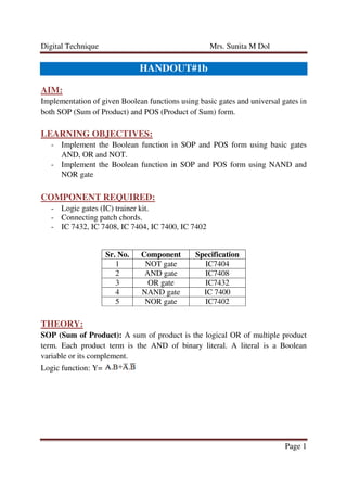
- 1. Digital Technique Mrs. Sunita M Dol Page 1 HANDOUT#1b AIM: Implementation of given Boolean functions using basic gates and universal gates in both SOP (Sum of Product) and POS (Product of Sum) form. LEARNING OBJECTIVES: - Implement the Boolean function in SOP and POS form using basic gates AND, OR and NOT. - Implement the Boolean function in SOP and POS form using NAND and NOR gate COMPONENT REQUIRED: - Logic gates (IC) trainer kit. - Connecting patch chords. - IC 7432, IC 7408, IC 7404, IC 7400, IC 7402 Sr. No. Component Specification 1 NOT gate IC7404 2 AND gate IC7408 3 OR gate IC7432 4 NAND gate IC 7400 5 NOR gate IC7402 THEORY: SOP (Sum of Product): A sum of product is the logical OR of multiple product term. Each product term is the AND of binary literal. A literal is a Boolean variable or its complement. Logic function: Y=
- 2. Digital Technique Mrs. Sunita M Dol Page 2 Truth table: A B AB 0 0 1 1 0 1 1 0 1 1 0 0 0 0 1 0 0 1 0 0 0 1 1 0 0 1 0 1 If we express the equation in SOP form then we can design the circuit using only NAND gate with the help of Demorgan’s Theorem and Logic function: Y= Truth table: A B AB 0 0 1 1 0 1 0 0 1 0 1 1 0 0 0 1 1 0 1 0 0 1 0 0 1 1 0 1 1 0 0 1 0 1 0 1
- 3. Digital Technique Mrs. Sunita M Dol Page 3 POS (Product of Sum): A product of sum is the logical AND of multiple sum term. Each sum term is the OR of binary literal. Logic function: Y= A B C (A+B) (B+C) 0 0 0 1 0 0 1 0 0 0 1 0 1 1 0 0 0 1 0 1 1 1 1 1 0 1 1 0 1 1 0 0 1 0 0 1 1 0 1 0 1 0 1 0 1 1 1 1 1 1 0 1 1 1 1 1 1 1 1 0 1 1 1 1
- 4. Digital Technique Mrs. Sunita M Dol Page 4 If we express the equation in POS form then we can design the circuit using only NOR gate with the help of Demorgan’s Theorem and Logic function: Y=
- 5. Digital Technique Mrs. Sunita M Dol Page 5 A B C (A+B) (B+C) Y 0 0 0 1 0 0 1 1 1 0 1 0 0 0 1 0 1 1 0 1 0 1 1 0 0 1 0 1 1 1 1 0 0 0 0 1 0 1 1 0 1 1 0 0 0 1 1 0 1 0 0 1 1 0 1 0 1 0 1 0 1 0 1 0 1 1 1 0 0 0 0 1 1 1 0 1 1 1 1 0 0 0 0 1 1 1 1 0 1 1 1 0 0 0 0 1 PROCEDURE: 1. Check the components for their working. 2. Insert the appropriate IC into the IC base. 3. Make connections as shown in the circuit diagram. 4. Provide the input data via the input switches and observe the output on output LEDs 5. Give various combinations of inputs and note down the output with help of LED for all gate ICs one by one. RESULT: Thus the given Boolean expression is implemented using basic logic gates AND, OR and NOT and universal gates NAND and NOR gates that is Y= Y=