SlideShare una empresa de Scribd logo
1 de 8
Bipolar Junction Transistor
Bipolar Transistor
• Diodes are made up from two pieces of semiconductor
material, either silicon or germanium to form a simple PN-
junction
• If we join together two individual signal diodes back-to-back,
this will give us two PN-junctions connected together in series
that share a common P or N terminal. The fusion of these two
diodes produces a three layer, two junction, three terminal
device forming the basis of a Bipolar Junction Transistor,
or BJT for short.
BJT Basics
Transistors are three terminal active devices made from
different semiconductor materials that can act as either an
insulator or a conductor by the application of a small signal
voltage. The transistor’s ability to change between these two
states enables it to have two basic functions: “switching”
(digital electronics) or “amplification” (analogue electronics).
Then bipolar transistor have the ability to operate within
three different regions:
• Active Region – the transistor operates as an amplifier
and Ic = β.Ib
• Saturation – the transistor is “Fully-ON” operating as a switch
and Ic = I(saturation)
• Cut-off – the transistor is “Fully-OFF” operating as a switch
and Ic = 0
Cont…
• The Bipolar Transistor basic construction consists of two
PN-junctions producing three connecting terminals with
each terminal being given a name to identify it from the
other two. These three terminals are known and labelled as
the Emitter ( E ), the Base ( B ) and the Collector ( C )
respectively.
• Bipolar Transistors are current regulating devices that
control the amount of current flowing through them in
proportion to the amount of biasing voltage applied to
their base terminal acting like a current-controlled switch.
The principle of operation of the two transistor
types PNP and NPN, is exactly the same the only difference
being in their biasing and the polarity of the power supply
for each type.
The construction and
circuit symbols for both
the PNP and NPN bipolar
transistor are given above
with the arrow in the
circuit symbol always
showing the direction of
“conventional current
flow” between the base
terminal and its emitter
terminal. The direction of
the arrow always points
from the positive P-type
region to the negative N-
type region for both
transistor types, exactly
the same as for the
standard diode symbol.
Bipolar Transistor Configurations
As the Bipolar Transistor is a three terminal device, there
are basically three possible ways to connect it within an
electronic circuit with one terminal being common to
both the input and output. Each method of connection
responding differently to its input signal within a circuit as
the static characteristics of the transistor vary with each
circuit arrangement.
• Common Base Configuration – has Voltage Gain but no
Current Gain.
• Common Emitter Configuration – has both Current and
Voltage Gain.
• Common Collector Configuration – has Current Gain but
no Voltage Gain.
CB, CE, CC Circuit configuration
CB
CE
CC
Comparison between CB, CE, CC
configuration

Más contenido relacionado

La actualidad más candente

Zener diode as a voltage Regulator
Zener diode as a voltage RegulatorZener diode as a voltage Regulator
Zener diode as a voltage RegulatorSanjaySingh011996
 
Electronics 1 : Chapter # 06 : Bipolar Junction Transistor
Electronics 1 : Chapter # 06 : Bipolar Junction TransistorElectronics 1 : Chapter # 06 : Bipolar Junction Transistor
Electronics 1 : Chapter # 06 : Bipolar Junction TransistorSk_Group
 
Bipolar junction transistor
Bipolar junction transistorBipolar junction transistor
Bipolar junction transistorArafat Hossan
 
Zener and avalanche diode
Zener and avalanche diode    Zener and avalanche diode
Zener and avalanche diode AnuJyothi2
 
Mosfet Operation and Charecteristics.
Mosfet Operation and Charecteristics.Mosfet Operation and Charecteristics.
Mosfet Operation and Charecteristics.Rafsan Rafin Khan
 
Field Effect Transistor (FET)
Field Effect Transistor (FET)Field Effect Transistor (FET)
Field Effect Transistor (FET)Jess Rangcasajo
 
Chapter-5- Transistor Characteristics-1.ppt
Chapter-5- Transistor Characteristics-1.pptChapter-5- Transistor Characteristics-1.ppt
Chapter-5- Transistor Characteristics-1.pptJeelBhanderi4
 
Diode v i characteristic
Diode v i characteristicDiode v i characteristic
Diode v i characteristicUnsa Shakir
 
Bipolar Junction Transistor (BJT).pptx
Bipolar Junction Transistor (BJT).pptxBipolar Junction Transistor (BJT).pptx
Bipolar Junction Transistor (BJT).pptxDarwin Nesakumar
 
Field Effect Transistor ppt
Field Effect Transistor pptField Effect Transistor ppt
Field Effect Transistor pptSameeksha Verma
 
Zener Diode Full Presentation
Zener Diode Full Presentation Zener Diode Full Presentation
Zener Diode Full Presentation Adeel Rasheed
 
Clampers and clippers
Clampers and clippersClampers and clippers
Clampers and clippersSARITHA REDDY
 

La actualidad más candente (20)

Diodes basics
Diodes   basicsDiodes   basics
Diodes basics
 
Transistor notes
Transistor notesTransistor notes
Transistor notes
 
Transistor
TransistorTransistor
Transistor
 
Mosfet
MosfetMosfet
Mosfet
 
BJT CB Configuration
BJT CB ConfigurationBJT CB Configuration
BJT CB Configuration
 
JFET
JFETJFET
JFET
 
Zener diode as a voltage Regulator
Zener diode as a voltage RegulatorZener diode as a voltage Regulator
Zener diode as a voltage Regulator
 
Electronics 1 : Chapter # 06 : Bipolar Junction Transistor
Electronics 1 : Chapter # 06 : Bipolar Junction TransistorElectronics 1 : Chapter # 06 : Bipolar Junction Transistor
Electronics 1 : Chapter # 06 : Bipolar Junction Transistor
 
Bipolar junction transistor
Bipolar junction transistorBipolar junction transistor
Bipolar junction transistor
 
Zener and avalanche diode
Zener and avalanche diode    Zener and avalanche diode
Zener and avalanche diode
 
Mosfet Operation and Charecteristics.
Mosfet Operation and Charecteristics.Mosfet Operation and Charecteristics.
Mosfet Operation and Charecteristics.
 
Field Effect Transistor (FET)
Field Effect Transistor (FET)Field Effect Transistor (FET)
Field Effect Transistor (FET)
 
Chapter-5- Transistor Characteristics-1.ppt
Chapter-5- Transistor Characteristics-1.pptChapter-5- Transistor Characteristics-1.ppt
Chapter-5- Transistor Characteristics-1.ppt
 
Diode v i characteristic
Diode v i characteristicDiode v i characteristic
Diode v i characteristic
 
Bipolar Junction Transistor (BJT).pptx
Bipolar Junction Transistor (BJT).pptxBipolar Junction Transistor (BJT).pptx
Bipolar Junction Transistor (BJT).pptx
 
Diode
DiodeDiode
Diode
 
Field Effect Transistor ppt
Field Effect Transistor pptField Effect Transistor ppt
Field Effect Transistor ppt
 
Zener Diode Full Presentation
Zener Diode Full Presentation Zener Diode Full Presentation
Zener Diode Full Presentation
 
Clampers and clippers
Clampers and clippersClampers and clippers
Clampers and clippers
 
nortons theorem.ppt
nortons theorem.pptnortons theorem.ppt
nortons theorem.ppt
 

Similar a Presentation bjt

Basic electronics,lecture 4
Basic electronics,lecture 4Basic electronics,lecture 4
Basic electronics,lecture 4Muhammad Ibrahim
 
PHY-Presentation.pptx
PHY-Presentation.pptxPHY-Presentation.pptx
PHY-Presentation.pptxMveTm
 
PowerPoint-Presentation-on-Active-components.pptx
PowerPoint-Presentation-on-Active-components.pptxPowerPoint-Presentation-on-Active-components.pptx
PowerPoint-Presentation-on-Active-components.pptxHarshalVaidya11
 
PowerPoint-Presentation-on-Active-components.pptx
PowerPoint-Presentation-on-Active-components.pptxPowerPoint-Presentation-on-Active-components.pptx
PowerPoint-Presentation-on-Active-components.pptxNIKUNJPATEL790213
 
Module II- Part 01.pptx
Module II- Part 01.pptxModule II- Part 01.pptx
Module II- Part 01.pptxssuseraaa4d6
 
Transistor Fundamentals
Transistor FundamentalsTransistor Fundamentals
Transistor FundamentalsJay Baria
 
BJT Basic and Biasing-Abridged(1).pptx
BJT Basic and Biasing-Abridged(1).pptxBJT Basic and Biasing-Abridged(1).pptx
BJT Basic and Biasing-Abridged(1).pptxNimishDuggal1
 
questões História do Tocantins- UFT/UFNT.pdf
questões História do Tocantins- UFT/UFNT.pdfquestões História do Tocantins- UFT/UFNT.pdf
questões História do Tocantins- UFT/UFNT.pdfprofvictorverano
 
What is a Power Transistor.pptx
What is a Power Transistor.pptxWhat is a Power Transistor.pptx
What is a Power Transistor.pptxyogeshkute
 
Bipolar junction Transistor.pptx
Bipolar junction Transistor.pptxBipolar junction Transistor.pptx
Bipolar junction Transistor.pptxdivya66307
 
Lecture UGYTYDRTYUBHYUJHBIUBH 10_BJT 1.pdf
Lecture UGYTYDRTYUBHYUJHBIUBH 10_BJT 1.pdfLecture UGYTYDRTYUBHYUJHBIUBH 10_BJT 1.pdf
Lecture UGYTYDRTYUBHYUJHBIUBH 10_BJT 1.pdfpremranjanv784
 

Similar a Presentation bjt (20)

Basic electronics,lecture 4
Basic electronics,lecture 4Basic electronics,lecture 4
Basic electronics,lecture 4
 
PHY-Presentation.pptx
PHY-Presentation.pptxPHY-Presentation.pptx
PHY-Presentation.pptx
 
PowerPoint-Presentation-on-Active-components.pptx
PowerPoint-Presentation-on-Active-components.pptxPowerPoint-Presentation-on-Active-components.pptx
PowerPoint-Presentation-on-Active-components.pptx
 
PowerPoint-Presentation-on-Active-components.pptx
PowerPoint-Presentation-on-Active-components.pptxPowerPoint-Presentation-on-Active-components.pptx
PowerPoint-Presentation-on-Active-components.pptx
 
Basic information
Basic informationBasic information
Basic information
 
Module II- Part 01.pptx
Module II- Part 01.pptxModule II- Part 01.pptx
Module II- Part 01.pptx
 
Bjt fundamentals
Bjt fundamentalsBjt fundamentals
Bjt fundamentals
 
Transistor Fundamentals
Transistor FundamentalsTransistor Fundamentals
Transistor Fundamentals
 
BJT Basic and Biasing-Abridged(1).pptx
BJT Basic and Biasing-Abridged(1).pptxBJT Basic and Biasing-Abridged(1).pptx
BJT Basic and Biasing-Abridged(1).pptx
 
Edcqnaunit 3 (1)
Edcqnaunit 3 (1)Edcqnaunit 3 (1)
Edcqnaunit 3 (1)
 
Edcqnaunit 3
Edcqnaunit 3Edcqnaunit 3
Edcqnaunit 3
 
questões História do Tocantins- UFT/UFNT.pdf
questões História do Tocantins- UFT/UFNT.pdfquestões História do Tocantins- UFT/UFNT.pdf
questões História do Tocantins- UFT/UFNT.pdf
 
Transistors
TransistorsTransistors
Transistors
 
What is a Power Transistor.pptx
What is a Power Transistor.pptxWhat is a Power Transistor.pptx
What is a Power Transistor.pptx
 
Bipolar junction Transistor.pptx
Bipolar junction Transistor.pptxBipolar junction Transistor.pptx
Bipolar junction Transistor.pptx
 
Lecture UGYTYDRTYUBHYUJHBIUBH 10_BJT 1.pdf
Lecture UGYTYDRTYUBHYUJHBIUBH 10_BJT 1.pdfLecture UGYTYDRTYUBHYUJHBIUBH 10_BJT 1.pdf
Lecture UGYTYDRTYUBHYUJHBIUBH 10_BJT 1.pdf
 
Chapter 4 bjt
Chapter 4 bjtChapter 4 bjt
Chapter 4 bjt
 
Transistor
TransistorTransistor
Transistor
 
Edc unit 3
Edc unit 3Edc unit 3
Edc unit 3
 
BJT.ppt
BJT.pptBJT.ppt
BJT.ppt
 

Último

Call Girls Narol 7397865700 Independent Call Girls
Call Girls Narol 7397865700 Independent Call GirlsCall Girls Narol 7397865700 Independent Call Girls
Call Girls Narol 7397865700 Independent Call Girlsssuser7cb4ff
 
Gurgaon ✡️9711147426✨Call In girls Gurgaon Sector 51 escort service
Gurgaon ✡️9711147426✨Call In girls Gurgaon Sector 51 escort serviceGurgaon ✡️9711147426✨Call In girls Gurgaon Sector 51 escort service
Gurgaon ✡️9711147426✨Call In girls Gurgaon Sector 51 escort servicejennyeacort
 
Sachpazis Costas: Geotechnical Engineering: A student's Perspective Introduction
Sachpazis Costas: Geotechnical Engineering: A student's Perspective IntroductionSachpazis Costas: Geotechnical Engineering: A student's Perspective Introduction
Sachpazis Costas: Geotechnical Engineering: A student's Perspective IntroductionDr.Costas Sachpazis
 
Arduino_CSE ece ppt for working and principal of arduino.ppt
Arduino_CSE ece ppt for working and principal of arduino.pptArduino_CSE ece ppt for working and principal of arduino.ppt
Arduino_CSE ece ppt for working and principal of arduino.pptSAURABHKUMAR892774
 
THE SENDAI FRAMEWORK FOR DISASTER RISK REDUCTION
THE SENDAI FRAMEWORK FOR DISASTER RISK REDUCTIONTHE SENDAI FRAMEWORK FOR DISASTER RISK REDUCTION
THE SENDAI FRAMEWORK FOR DISASTER RISK REDUCTIONjhunlian
 
Main Memory Management in Operating System
Main Memory Management in Operating SystemMain Memory Management in Operating System
Main Memory Management in Operating SystemRashmi Bhat
 
Mine Environment II Lab_MI10448MI__________.pptx
Mine Environment II Lab_MI10448MI__________.pptxMine Environment II Lab_MI10448MI__________.pptx
Mine Environment II Lab_MI10448MI__________.pptxRomil Mishra
 
CCS355 Neural Networks & Deep Learning Unit 1 PDF notes with Question bank .pdf
CCS355 Neural Networks & Deep Learning Unit 1 PDF notes with Question bank .pdfCCS355 Neural Networks & Deep Learning Unit 1 PDF notes with Question bank .pdf
CCS355 Neural Networks & Deep Learning Unit 1 PDF notes with Question bank .pdfAsst.prof M.Gokilavani
 
Input Output Management in Operating System
Input Output Management in Operating SystemInput Output Management in Operating System
Input Output Management in Operating SystemRashmi Bhat
 
Correctly Loading Incremental Data at Scale
Correctly Loading Incremental Data at ScaleCorrectly Loading Incremental Data at Scale
Correctly Loading Incremental Data at ScaleAlluxio, Inc.
 
Past, Present and Future of Generative AI
Past, Present and Future of Generative AIPast, Present and Future of Generative AI
Past, Present and Future of Generative AIabhishek36461
 
Internet of things -Arshdeep Bahga .pptx
Internet of things -Arshdeep Bahga .pptxInternet of things -Arshdeep Bahga .pptx
Internet of things -Arshdeep Bahga .pptxVelmuruganTECE
 
Research Methodology for Engineering pdf
Research Methodology for Engineering pdfResearch Methodology for Engineering pdf
Research Methodology for Engineering pdfCaalaaAbdulkerim
 
IVE Industry Focused Event - Defence Sector 2024
IVE Industry Focused Event - Defence Sector 2024IVE Industry Focused Event - Defence Sector 2024
IVE Industry Focused Event - Defence Sector 2024Mark Billinghurst
 
US Department of Education FAFSA Week of Action
US Department of Education FAFSA Week of ActionUS Department of Education FAFSA Week of Action
US Department of Education FAFSA Week of ActionMebane Rash
 
Energy Awareness training ppt for manufacturing process.pptx
Energy Awareness training ppt for manufacturing process.pptxEnergy Awareness training ppt for manufacturing process.pptx
Energy Awareness training ppt for manufacturing process.pptxsiddharthjain2303
 
National Level Hackathon Participation Certificate.pdf
National Level Hackathon Participation Certificate.pdfNational Level Hackathon Participation Certificate.pdf
National Level Hackathon Participation Certificate.pdfRajuKanojiya4
 
The SRE Report 2024 - Great Findings for the teams
The SRE Report 2024 - Great Findings for the teamsThe SRE Report 2024 - Great Findings for the teams
The SRE Report 2024 - Great Findings for the teamsDILIPKUMARMONDAL6
 

Último (20)

Call Girls Narol 7397865700 Independent Call Girls
Call Girls Narol 7397865700 Independent Call GirlsCall Girls Narol 7397865700 Independent Call Girls
Call Girls Narol 7397865700 Independent Call Girls
 
Gurgaon ✡️9711147426✨Call In girls Gurgaon Sector 51 escort service
Gurgaon ✡️9711147426✨Call In girls Gurgaon Sector 51 escort serviceGurgaon ✡️9711147426✨Call In girls Gurgaon Sector 51 escort service
Gurgaon ✡️9711147426✨Call In girls Gurgaon Sector 51 escort service
 
🔝9953056974🔝!!-YOUNG call girls in Rajendra Nagar Escort rvice Shot 2000 nigh...
🔝9953056974🔝!!-YOUNG call girls in Rajendra Nagar Escort rvice Shot 2000 nigh...🔝9953056974🔝!!-YOUNG call girls in Rajendra Nagar Escort rvice Shot 2000 nigh...
🔝9953056974🔝!!-YOUNG call girls in Rajendra Nagar Escort rvice Shot 2000 nigh...
 
Sachpazis Costas: Geotechnical Engineering: A student's Perspective Introduction
Sachpazis Costas: Geotechnical Engineering: A student's Perspective IntroductionSachpazis Costas: Geotechnical Engineering: A student's Perspective Introduction
Sachpazis Costas: Geotechnical Engineering: A student's Perspective Introduction
 
Arduino_CSE ece ppt for working and principal of arduino.ppt
Arduino_CSE ece ppt for working and principal of arduino.pptArduino_CSE ece ppt for working and principal of arduino.ppt
Arduino_CSE ece ppt for working and principal of arduino.ppt
 
THE SENDAI FRAMEWORK FOR DISASTER RISK REDUCTION
THE SENDAI FRAMEWORK FOR DISASTER RISK REDUCTIONTHE SENDAI FRAMEWORK FOR DISASTER RISK REDUCTION
THE SENDAI FRAMEWORK FOR DISASTER RISK REDUCTION
 
Main Memory Management in Operating System
Main Memory Management in Operating SystemMain Memory Management in Operating System
Main Memory Management in Operating System
 
Mine Environment II Lab_MI10448MI__________.pptx
Mine Environment II Lab_MI10448MI__________.pptxMine Environment II Lab_MI10448MI__________.pptx
Mine Environment II Lab_MI10448MI__________.pptx
 
CCS355 Neural Networks & Deep Learning Unit 1 PDF notes with Question bank .pdf
CCS355 Neural Networks & Deep Learning Unit 1 PDF notes with Question bank .pdfCCS355 Neural Networks & Deep Learning Unit 1 PDF notes with Question bank .pdf
CCS355 Neural Networks & Deep Learning Unit 1 PDF notes with Question bank .pdf
 
Input Output Management in Operating System
Input Output Management in Operating SystemInput Output Management in Operating System
Input Output Management in Operating System
 
Correctly Loading Incremental Data at Scale
Correctly Loading Incremental Data at ScaleCorrectly Loading Incremental Data at Scale
Correctly Loading Incremental Data at Scale
 
Past, Present and Future of Generative AI
Past, Present and Future of Generative AIPast, Present and Future of Generative AI
Past, Present and Future of Generative AI
 
Internet of things -Arshdeep Bahga .pptx
Internet of things -Arshdeep Bahga .pptxInternet of things -Arshdeep Bahga .pptx
Internet of things -Arshdeep Bahga .pptx
 
Research Methodology for Engineering pdf
Research Methodology for Engineering pdfResearch Methodology for Engineering pdf
Research Methodology for Engineering pdf
 
IVE Industry Focused Event - Defence Sector 2024
IVE Industry Focused Event - Defence Sector 2024IVE Industry Focused Event - Defence Sector 2024
IVE Industry Focused Event - Defence Sector 2024
 
US Department of Education FAFSA Week of Action
US Department of Education FAFSA Week of ActionUS Department of Education FAFSA Week of Action
US Department of Education FAFSA Week of Action
 
young call girls in Green Park🔝 9953056974 🔝 escort Service
young call girls in Green Park🔝 9953056974 🔝 escort Serviceyoung call girls in Green Park🔝 9953056974 🔝 escort Service
young call girls in Green Park🔝 9953056974 🔝 escort Service
 
Energy Awareness training ppt for manufacturing process.pptx
Energy Awareness training ppt for manufacturing process.pptxEnergy Awareness training ppt for manufacturing process.pptx
Energy Awareness training ppt for manufacturing process.pptx
 
National Level Hackathon Participation Certificate.pdf
National Level Hackathon Participation Certificate.pdfNational Level Hackathon Participation Certificate.pdf
National Level Hackathon Participation Certificate.pdf
 
The SRE Report 2024 - Great Findings for the teams
The SRE Report 2024 - Great Findings for the teamsThe SRE Report 2024 - Great Findings for the teams
The SRE Report 2024 - Great Findings for the teams
 

Presentation bjt

  • 2. Bipolar Transistor • Diodes are made up from two pieces of semiconductor material, either silicon or germanium to form a simple PN- junction • If we join together two individual signal diodes back-to-back, this will give us two PN-junctions connected together in series that share a common P or N terminal. The fusion of these two diodes produces a three layer, two junction, three terminal device forming the basis of a Bipolar Junction Transistor, or BJT for short.
  • 3. BJT Basics Transistors are three terminal active devices made from different semiconductor materials that can act as either an insulator or a conductor by the application of a small signal voltage. The transistor’s ability to change between these two states enables it to have two basic functions: “switching” (digital electronics) or “amplification” (analogue electronics). Then bipolar transistor have the ability to operate within three different regions: • Active Region – the transistor operates as an amplifier and Ic = β.Ib • Saturation – the transistor is “Fully-ON” operating as a switch and Ic = I(saturation) • Cut-off – the transistor is “Fully-OFF” operating as a switch and Ic = 0
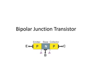
  • 4. Cont… • The Bipolar Transistor basic construction consists of two PN-junctions producing three connecting terminals with each terminal being given a name to identify it from the other two. These three terminals are known and labelled as the Emitter ( E ), the Base ( B ) and the Collector ( C ) respectively. • Bipolar Transistors are current regulating devices that control the amount of current flowing through them in proportion to the amount of biasing voltage applied to their base terminal acting like a current-controlled switch. The principle of operation of the two transistor types PNP and NPN, is exactly the same the only difference being in their biasing and the polarity of the power supply for each type.
  • 5. The construction and circuit symbols for both the PNP and NPN bipolar transistor are given above with the arrow in the circuit symbol always showing the direction of “conventional current flow” between the base terminal and its emitter terminal. The direction of the arrow always points from the positive P-type region to the negative N- type region for both transistor types, exactly the same as for the standard diode symbol.
  • 6. Bipolar Transistor Configurations As the Bipolar Transistor is a three terminal device, there are basically three possible ways to connect it within an electronic circuit with one terminal being common to both the input and output. Each method of connection responding differently to its input signal within a circuit as the static characteristics of the transistor vary with each circuit arrangement. • Common Base Configuration – has Voltage Gain but no Current Gain. • Common Emitter Configuration – has both Current and Voltage Gain. • Common Collector Configuration – has Current Gain but no Voltage Gain.
  • 7. CB, CE, CC Circuit configuration CB CE CC
  • 8. Comparison between CB, CE, CC configuration