1. LCD-016M002B
Vishay
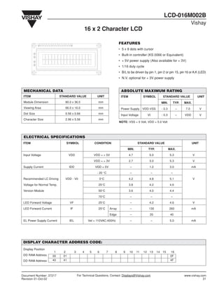
16 x 2 Character LCD
FEATURES
• 5 x 8 dots with cursor
• Built-in controller (KS 0066 or Equivalent)
• + 5V power supply (Also available for + 3V)
• 1/16 duty cycle
• B/L to be driven by pin 1, pin 2 or pin 15, pin 16 or A.K (LED)
• N.V. optional for + 3V power supply
MECHANICAL DATA ABSOLUTE MAXIMUM RATING
ITEM STANDARD VALUE UNIT ITEM SYMBOL STANDARD VALUE UNIT
Module Dimension 80.0 x 36.0 mm MIN. TYP. MAX.
Viewing Area 66.0 x 16.0 mm Power Supply VDD-VSS - 0.3 – 7.0 V
Dot Size 0.56 x 0.66 mm Input Voltage VI - 0.3 – VDD V
Character Size 2.96 x 5.56 mm
NOTE: VSS = 0 Volt, VDD = 5.0 Volt
ELECTRICAL SPECIFICATIONS
ITEM SYMBOL CONDITION STANDARD VALUE UNIT
MIN. TYP. MAX.
Input Voltage VDD VDD = + 5V 4.7 5.0 5.3 V
VDD = + 3V 2.7 3.0 5.3 V
Supply Current IDD VDD = 5V – 1.2 3.0 mA
- 20 °C – – –
Recommended LC Driving VDD - V0 0°C 4.2 4.8 5.1 V
Voltage for Normal Temp. 25°C 3.8 4.2 4.6
Version Module 50°C 3.6 4.0 4.4
70°C – – –
LED Forward Voltage VF 25°C – 4.2 4.6 V
LED Forward Current IF 25°C Array – 130 260 mA
Edge – 20 40
EL Power Supply Current IEL Vel = 110VAC:400Hz – – 5.0 mA
DISPLAY CHARACTER ADDRESS CODE:
Display Position
1 2 3 4 5 6 7 8 9 10 11 12 13 14 15 16
DD RAM Address 00 01 0F
DD RAM Address 40 41 4F
Document Number: 37217 For Technical Questions, Contact: Displays@Vishay.com www.vishay.com
Revision 01-Oct-02 31
2. LCD-016M002B
Vishay 16 x 2 Character LCD
PIN NUMBER SYMBOL FUNCTION
1 Vss GND
2 Vdd + 3V or + 5V
3 Vo Contrast Adjustment
4 RS H/L Register Select Signal
5 R/W H/L Read/Write Signal
6 E H → L Enable Signal
7 DB0 H/L Data Bus Line
8 DB1 H/L Data Bus Line
9 DB2 H/L Data Bus Line
10 DB3 H/L Data Bus Line
11 DB4 H/L Data Bus Line
12 DB5 H/L Data Bus Line
13 DB6 H/L Data Bus Line
14 DB7 H/L Data Bus Line
15 A/Vee + 4.2V for LED/Negative Voltage Output
16 K Power Supply for B/L (OV)
DIMENSIONS in millimeters
3.55
2.95 0.6
0.6
0.55
DOT SIZE
0.65
0.7
5.55
5.95
80.0 ± 0.5
0.4
4.95 71.2
7.55 66.0 (VA)
12.45 56.2 (AA)
11.76
12.55
15.76
8.0 P2.54* 15 = 38.1 H1 MAX 9.7 MAX
2.5
5.2
2.5
9.8
3.0 1.8 16 Ø 1.0 PTH H2 5.1
1 16
18.3
K
36.0 ± 0.5
11.5 (AA)
16.0 (VA)
25.2
31.0
5.08
13.08
A
4 Ø 1.0 40.55 4-Ø 2.5 PTH 1.6 1.6
2.5 75.0 4-Ø 5.0 PAD EL OR NO B/L
LED - H/L B/L
HIGH LOW
H1 13.2 12.1
H2 8.6 7.5
www.vishay.com For Technical Questions, Contact: Displays@Vishay.com Document Number: 37217
32 Revision 01-Oct-02
3. This datasheet has been download from:
www.datasheetcatalog.com
Datasheets for electronics components.