Connector Corner: Accelerate revenue generation using UiPath API-centric busi...
Vanzee 1201
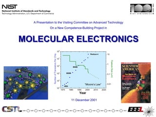
1. A Presentation to the Visiting Committee on Advanced Technology
On a New Competence-Building Project in
MOLECULAR ELECTRONICS
8
10
Number of Transistors Per Chip Pentium 4 10
7
10
Feature Size (µm)
6
1
10 80486
5
10 80286
0.1
4
10
“Moore’s Law” 0.01
4004
3
10
1970 1980 1990 2000 2010 2020
Year
11 December 2001
2. Molecular Electronics?
•What is “Molecular Electronics?”
•Why now?
•Who are the players?
•How can NIST help?
•Our team approach.
•The first year’s progress.
•The road ahead.
3. Molecular Electronics
— moletronics —
A new technology that uses molecules to
perform the function of electronic components.
wire
amplifier
A
diode
switch
NO2
SH
H2N
D
5. Moletronic Components
Transistors
Lucent Electrically-Active Memory
Molecules S
MEC, Harvard
Rice, Univ. of Alabama, UCLA
junction diode N
C
C H33
16 N
C C
N N
O O O O
O + N N + RTD
Logic Function S S
S S
Hewlett-Packard, UCLA, Mitre Corp. O + N
O
N +
S
Nanotube FET
O
Vc O O IBM
V1 switch
V2
Vout
“I was one of the biggest skeptics. Now I believe that this is the
inevitable wave of the future.” —R. S. Williams, Hewlett-Packard
6. Approaching Fundamental Limits
8
10
Computational Paradigm Shifts Moore’s Law Pentium 4 10
1644
Transistors per Chip
7
10
1945
Feature Size (µm)
1
ENIAC 6
10 80486
5
10 80286
0.1
4
10
1948 0.01
4004 Device Physics Changes
3
10
1970 1980 1990 2000 2010 2020
1959
Year
Transistor
0.013 µm
A new components technology is required
IC 2016 to maintain the uninterrupted succession
of smaller and faster electronic devices.
7. Why Use Molecules?
• Even big molecules are small.
• Functional control through synthesis.
• Self-assembling devices.
10µ
Classical
1µ
Linewidth (m)
NO2 NH2
100n
H2N NO2
10n
Molecular
Quantum Lengths
1n
1970 1980 1990 2000 2010 2020
Year
HS - R - X S S
NDR R
NDR – Negative Differential Resistance
metal R – Resistor
10 nm
8. How Molecules Conduct
Conventional Electronics Molecular Electronics
–S—CH2—CH2—CH2 — S –
insulator
insulator
–S—CH —C —CH — S –
conductor conductor
–S—CAc —C —CDn — S –
doped semiconductors
substituted molecules
9. Moletronic Components
Transistors
Lucent Electrically-Active
S
Memory
Molecules MEC, Harvard
Rice, Univ. of Alabama, UCLA
N
C
C H33
16 N
C C
N N
junction diode RTD
Logic Function
Hewlett-Packard, UCLA, Mitre Corp. O O O O S
Vc O + N
S S
N +
Nanotube FET
V1 S S
+
IBM
O + N N
O
V2 O
O O
Vout switch
“I was one of the biggest skeptics. Now I believe that this is the
inevitable wave of the future.” — R. S. Williams, Hewlett-Packard
10. A Role for NIST
To develop the measurement tools and
data necessary to measure, model, and
control the flow of charge through
molecules and ensembles of molecules.
“To knowledge by measurement.”
— Kammerlingh Onnes, Leiden Univ.
11. Grand Challenges
•Develop Moletronics Metrology
• Correlate Structure and Function
Science, vol. 286, p. 1551
Sci. Am. June 2000
“The field suffers from an excess of imagination and a deficiency
of accomplishment.” —J. Hopfield, Princeton University
12. Our Role/The Challenge
— What does it mean? How do to make it useful? —
•What is the physical basis for
electrical activity in
moletronic systems?
•How are electrical quantities
reliably measured at
molecular dimensions?
•What measurements and data
are needed to speed this
technology to market?
13. Our Goals
• To advance the measurement sciences and
standards as applied to moletronics.
– Quantitative measurement and understanding
of molecular conductance
– Validated models
– Characterized prototype
– Test vehicle for molecular components
• To create a nucleation center for speeding
the development of moletronics technology.
“New directions in science are launched by new tools much more
often than by new concepts.” — Dudley Herschbach, Harvard Univ.
14. A Multidisciplinary Effort
Chemistry Electrical Engineering
•Self-Assembly •Contacts
•Structure •Integration
•Mechanisms •Performance
•Modeling •Reliability
S. Robey
S. Robey
M. Tarlov
M. Tarlov R. van Zee
R. van Zee
R. van Zee
R. van Zee J. Suehle
J. Suehle
C. Richter
C. Richter
C. Gonzalez
C. Gonzalez
C. Richter
C. Richter
15. Research Emphases
Electrical Properties of Structure of Electrically-
Small Ensembles Active, Molecular Films
NO2 NO2 NO2 NO2 NO2 NO2 NO2
NO2 NO2 NO2 NO2 NO2 NO2 NO2
NH2 NH2 NH2 NH2 NH2 NH2 NH2
NH2 NH2 NH2 NH2 NH2 NH2 NH2
S S S S S S S
S S S S S S S
NO2 NO2 NO2 NO2 NO2
NO2 2e2T2
g(E) = ∆D ∆ A
NH2 NH2 NH2 NH2 NH2
NH2
πhγ2
S S S S S
S
Electrical Properties of
Theory Large Ensembles
16. Resistance of Small Ensembles
- Studying Film Structure -
p-benzenedimethanethiol
SH
In KBr Pellet
CH2 Resistance
18 MΩ ± 12 MΩ
Grown in Solution
CH2 Grown from Vapor
R.P. Andres et al., Purdue
SH Science, 272, p.1323
1000 1500 -1
2000
wavenumber (cm )
A.M. Bratkovsky, HPRL
Phys. Rev. B, 64, 195413
Conduction
SH
SH SH SH SH SH SH CH2
CH2 CH2 CH2 CH2 CH2 CH2
CH2 CH2 CH2 CH2 CH2 CH2
CH2
S S S S S S angle
S
0 30 60 90
Angle
17. From Molecules to Devices
- Building Test Structures -
Top Electrode
Field SiO2
Ultra-thin SiO2
Bottom Electrode 2 nm - 10 nm
SiO2/Si3N4
Low Temp. Au
Top Electrode
NO2 NO2 NO2 NO2 NO2 Molecular Length
(2 nm – 10 nm)
NH2 NH2 NH2 NH2 NH2
S S S S S
Bottom Electrode
~20 µm
~40 nm No. of Molecules
(10 nm - 100 nm)
18. Testing Device Performance
- Reliable Electrical Measurements -
Device Operating
0.75 Characteristics
Capacitance (pF)
0.74
Cross
Bars 0.73
0.72
Al
Probe Station 40 “1”
Ti High
30
current
Current (pA)
CH3(CH2)18CO2H 20 “0”
Low
HO HO HO HO HO HO HO HO HO HO HO HO HO HO HO HO
O O O O O O O O O O O O O O O O
Al2O3 10
current
Al 0
-2 -1 0 1 2 3 4
Applied Voltage (V) D.R. Stewart et al., HPRL
Bull. Am. Phys. Soc., 46, p.1
19. Modeling Molecular Switches
- Understanding Electrical Function and Molecular Structure -
0.2
Charge on Rings
Kohn-Sham Equations
Charge on Rings (AU)
Upper Ring - RU
Middle Ring - RM RU
Lower Ring - RL 0.1
F[p(r)] = Ehf [p(r)] + Ex [p(r)] NO2
Current
RM
NH2
{T+Vhf(r)+Vn(r) + Vx(r)} ϕi = ε ϕ i 0.0
RL
S
-0.1
0.0 0.5 1.0 1.5 2.0 2.5
Applied Voltage (V)
• Significant charge density localization at
voltages below 2.1 V (no current). –S—RL—RM—RU <2.1 V
• Near 2.1 V maximum de-localization of
charge density (maximum current). –S—RL —RM —RU ~2.1 V
• Above 2.1 V charge density localization –S—RL—RM—RU >2.1 V
occurs again (no current).
21. Leveraging our Resources
•Nanocell Molecular Computer Collaboratory
(Molecules, Electrical Characterization)
–J. M. Tour, Rice University
–M.A. Reed, Yale University
–P.S. Weiss, Penn State University
•Hewlett-Packard Research Labs
(Devices, Electronic Structure)
–R.S. Williams
–P.J. Kuekes
•Naval Research Laboratory
(Molecules)
–R. Shashidhar
22. Molecular Electronics!
•Important Technology
•Revolutionary
•Timely
•Critical Role for NIST
•Interdisciplinary Team
•Strong Partnerships with
Industry & Universities
Strategies for Success