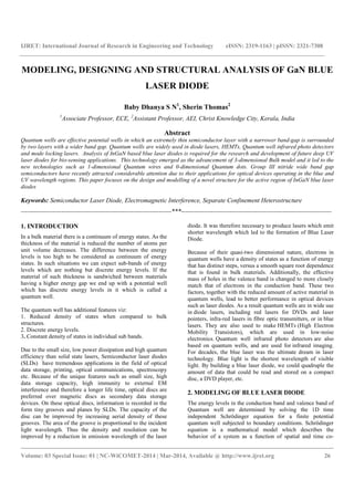
Modeling, designing and structural analysis of ga n blue
•
1 recomendación•221 vistas


Recomendados
Recomendados
Más contenido relacionado
La actualidad más candente
La actualidad más candente (19)
Destacado
Destacado (20)
Similar a Modeling, designing and structural analysis of ga n blue
Similar a Modeling, designing and structural analysis of ga n blue (20)
Más de eSAT Publishing House
Más de eSAT Publishing House (20)
Último
Último (20)
Modeling, designing and structural analysis of ga n blue
- 1. IJRET: International Journal of Research in Engineering and Technology eISSN: 2319-1163 | pISSN: 2321-7308 __________________________________________________________________________________________ Volume: 03 Special Issue: 01 | NC-WiCOMET-2014 | Mar-2014, Available @ http://www.ijret.org 26 MODELING, DESIGNING AND STRUCTURAL ANALYSIS OF GaN BLUE LASER DIODE Baby Dhanya S N1 , Sherin Thomas2 1 Associate Professor, ECE, 2 Assistant Professor, AEI, Christ Knowledge City, Kerala, India Abstract Quantum wells are effective potential wells in which an extremely thin semiconductor layer with a narrower band-gap is surrounded by two layers with a wider band gap. Quantum wells are widely used in diode lasers, HEMTs, Quantum well infrared photo detectors and mode locking lasers. Analysis of InGaN based blue laser diodes is required for the research and development of future deep UV laser diodes for bio-sensing applications. This technology emerged as the advancement of 3-dimensional Bulk model and it led to the new technologies such as 1-dimensional Quantum wires and 0-dimensional Quantum dots. Group III nitride wide band gap semiconductors have recently attracted considerable attention due to their applications for optical devices operating in the blue and UV wavelength regions. This paper focuses on the design and modelling of a novel structure for the active region of InGaN blue laser diodes Keywords: Semiconductor Laser Diode, Electromagnetic Interference, Separate Confinement Heterostructure -----------------------------------------------------------------------***----------------------------------------------------------------------- 1. INTRODUCTION In a bulk material there is a continuum of energy states. As the thickness of the material is reduced the number of atoms per unit volume decreases. The difference between the energy levels is too high to be considered as continuum of energy states. In such situations we can expect sub-bands of energy levels which are nothing but discrete energy levels. If the material of such thickness is sandwiched between materials having a higher energy gap we end up with a potential well which has discrete energy levels in it which is called a quantum well. The quantum well has additional features viz: 1. Reduced density of states when compared to bulk structures. 2. Discrete energy levels. 3. Constant density of states in individual sub bands. Due to the small size, low power dissipation and high quantum efficiency than solid state lasers, Semiconductor laser diodes (SLDs) have tremendous applications in the field of optical data storage, printing, optical communications, spectroscopy etc. Because of the unique features such as small size, high data storage capacity, high immunity to external EM interference and therefore a longer life time, optical discs are preferred over magnetic discs as secondary data storage devices. On these optical discs, information is recorded in the form tiny grooves and planes by SLDs. The capacity of the disc can be improved by increasing aerial density of these grooves. The area of the groove is proportional to the incident light wavelength. Thus the density and resolution can be improved by a reduction in emission wavelength of the laser diode. It was therefore necessary to produce lasers which emit shorter wavelength which led to the formation of Blue Laser Diode. Because of their quasi-two dimensional nature, electrons in quantum wells have a density of states as a function of energy that has distinct steps, versus a smooth square root dependence that is found in bulk materials. Additionally, the effective mass of holes in the valence band is changed to more closely match that of electrons in the conduction band. These two factors, together with the reduced amount of active material in quantum wells, lead to better performance in optical devices such as laser diodes. As a result quantum wells are in wide use in diode lasers, including red lasers for DVDs and laser pointers, infra-red lasers in fibre optic transmitters, or in blue lasers. They are also used to make HEMTs (High Electron Mobility Transistors), which are used in low-noise electronics. Quantum well infrared photo detectors are also based on quantum wells, and are used for infrared imaging. For decades, the blue laser was the ultimate dream in laser technology. Blue light is the shortest wavelength of visible light. By building a blue laser diode, we could quadruple the amount of data that could be read and stored on a compact disc, a DVD player, etc. 2. MODELING OF BLUE LASER DIODE The energy levels in the conduction band and valence band of Quantum well are determined by solving the 1D time independent Schrödinger equation for a finite potential quantum well subjected to boundary conditions. Schrödinger equation is a mathematical model which describes the behavior of a system as a function of spatial and time co-
- 2. IJRET: International Journal of Research in Engineering and Technology eISSN: 2319-1163 | pISSN: 2321-7308 __________________________________________________________________________________________ Volume: 03 Special Issue: 01 | NC-WiCOMET-2014 | Mar-2014, Available @ http://www.ijret.org 27 ordinates in terms of a wave function Ψ. solving the Schrödinger equation in time independent form gives the possible wave functions that can exist within the region. Different Ψ functions give the possible energy levels in the region. Time Independent Schrodinger Equation is given by: E is the energy of the system. Carriers at the edge of energy bands follow a parabolic E-k relationship. They behave as free carriers as observed for uniform potentials. The carriers encounter no potentials inside the well. The carriers encounter potential barriers, Vo, at the extremes of the low band gap semiconductor. Substituting, The equation becomes, This gives Outside the well, (x) = 0 and (x) = A sinkx. Putting x = a, where a is the thickness of quantum well, gives Thus the equation becomes, This equation gives the energy levels in a quantum well. The energy levels for different values of n can be plotted as shown below: Fig- 1 Energy levels in quantum well The wave functions can be plotted by giving, which gives the equation, Blue laser diodes emit light in the wavelength of range 440nm- 485nm. This region of operation has led to applications in optical data storage i.e. in CDs and DVDs and high resolution printing. Emission of photons in the blue region requires a material having a band gap of 2.64ev. Fig -2 Wave functions in quantum well 3. DESIGNING OF BLUE LASER DIODE This band gap can also be tailored by alloying wide band gap (>2.4ev) materials. The materials under investigation were group III-V, II-V1, and SiC investigation as they possessed sufficient energy gap for emission in the blue region. Experimental results showed that laser diodes fabricated using GaN had high internal quantum efficiency and longer life time inspite of having a high dislocation density. These results led to the commercialization of GaN based blue laser diodes. Thus InGaN is used as the active region and AlGaN as the cladding region. For the effective electrical confinement of optical field in SCH structure, the refractive index difference between core
- 3. IJRET: International Journal of Research in Engineering and Technology eISSN: 2319-1163 | pISSN: 2321-7308 __________________________________________________________________________________________ Volume: 03 Special Issue: 01 | NC-WiCOMET-2014 | Mar-2014, Available @ http://www.ijret.org 28 and cladding must be very high. The proposed structure is shown below: Fig- 3 Proposed structure Laser diodes with different design layout have been fabricated and most of the designs reported were SCH devices which had multiple quantum wells as the active region with GaN as the optical guiding region and AlGaN layer as the cladding region .Additionally there is an electron blocking p-AlGaN layer which prevented overflow of electrons. Laser diodes with different emission wavelengths, efficiencies, output powers and threshold currents were reported by varying the properties of each of these layers. The active region consisting of InGaN quantum wells is responsible for confining the carriers. The proposed model is an SCH structure with InGaN MQW as the active region, GaN as optical guiding region and AlGaN as the cladding region for emission wavelength in the range of 440nm – 485nm. Multiple quantum wells are used to increase the amount of power emitted by the laser diode as the power generated by a single quantum well is limited by the saturation effects. 4. STRUCTURAL ANALYSIS OF BLUE LASER DIODE When the InGaN quantum well is of thickness comparable to the scattering length of the carriers the carriers do not thermalize sufficiently to settle down at lower energy states. In order to increase the fraction of carriers settling down at lower energy states a higher carrier density is needed. This implies an increase in the threshold current density of the laser diode. Multiple quantum wells solve this problem to some extent. Coupling of a quantum via a thin barrier to another barrier increases the effective length of the active region. To get a uniform distribution of carriers in the quantum wells if the effective mass of the electrons in the quantum wells close to the n – side is increased and the effective mass of holes in the quantum wells is reduced then we can have a uniformity in the distribution of carriers across the active region. If uniformity is achieved the AlGaN blocking layer responsible for preventing the carriers from overflowing can be removed. The problem with AlGaN blocking layer is that it prevents the overflow of carriers(electrons) at the cost of increased series resistance and also presents a barrier to the free flow of holes into the quantum well from the p-region. A double barrier quantum well formed by placing a wider quantum well above a narrow quantum well can reduce the carrier overflow and thereby causes a reduction in the threshold current density of the laser diode. A 1D – photonic crystal is composed of alternating stacks of layers having a low and high index of refraction. These structures reflect light at any polarizations, any incidence angle and over a wide range of wavelengths. The emission in a quantum well is dominated by the difference in energy levels between the lowest discrete energy level in the conduction band and the highest discrete energy level in the valence band. The discrete energy levels in the conduction and valence band are given are given by solving the Schrödinger time independent wave equation for both the potential wells in the conduction band and valence band respectively. As most of the carriers settle down into the lowest energy level the emission energy is dominated by lower energy levels. The emission wavelength is dependent on the position of the energy levels relative to the band edge. 5. SIMULATION OF QUANTUM WELL IN BLUE LASER DIODE The wave functions and energy levels of InGaN quantum well of thickness 60 micrometers have been simulated using Matlab. The output is obtained by solving 1D Schrodinger equation for a finite potential well. The quantum well thickness in micrometer unit is taken along x-axis. Along y- axis two parameters are taken: the energy of quantum well in eV unit and the wavefunction. The equation for energy has been obtained as: From the equation, it is clear that E depends only on the no. of energy levels as all the other parameters are constant. Thus for different values of n=1,2,3 and 4, different energy levels has been plotted. Also the equation for wave function gas been obtained as: Here also, the wave functions depend only on the value of n as all other parameters are constant. Hence wave functions have been plotted for values of n=1,2,3 and 4. The graph obtained using matlab is shown below:
- 4. IJRET: International Journal of Research in Engineering and Technology eISSN: 2319-1163 | pISSN: 2321-7308 __________________________________________________________________________________________ Volume: 03 Special Issue: 01 | NC-WiCOMET-2014 | Mar-2014, Available @ http://www.ijret.org 29 Fig - 4 Energy level and Wave functions in InGaN quantum well simulated using Matlab A p-n junction semiconductor laser diode has the disadvantage of improper optical confinement, leading to heavy losses. So a large current was required for the lasing action. A Double Heterostructure Laser Diode (DHLD) formed by sandwiching a lower band gap material in between two higher band gap materials was a solution to this problem to an extent. When forward biased, the injected carriers were trapped in the potential well formed by the structure, thereby preventing the loss of carriers. As the thickness of this potential well decreased, the lasing action was found to be obtained at lower threshold current densities which was the formation of quantum well laser diode. Thus the blue laser diode was obtained. 6. CONCLUSIONS Designs for the active region have been proposed to achieve uniform distribution of carriers across the active region of the quantum well to achieve lasing at low energies at a threshold current density compared to the conventional laser diode structures. These designs can also be applied to InGaN LEDs to prevent the overflow of carriers in the proposed quantum well laser diode structures. These results can be applied towards research and development of AlInGaN deep UV laser diodes. As for the future work, InGaN laser diodes based on the proposed structure have to be grown and tested. The parameters like quantum well thickness, barrier thickness have to be varied to get the lowest threshold current density for the laser diode that is the optimum laser diode design. REFERENCES [1]. Ben G. Streetman, Sanjay Kumar Banerjee, "Solid State electronic devices" ,Pearson Education Inc., 2008 [2]. Bahaa E. A. Saleh,"Fundamentals of Photonics", John Wiley and Sons,Inc 1991. [3]. Larry A Coldren, Scott W.Corzine, "Diode Lasers and Photonic", Wiley and Sons,Inc 1995. [4]. Nick Holonyak Jr, Robert M Kolbas, Daniel Dapkus, IEEE Journal of Quantum Electronics, VOl,QE-16,No 2,February 1980. [5]. John T. Torvik, Jacques I. Pankove, Bart J. Van Zeghbroeck, IEEE Transactions on Electron Devices, 46 (7), 1999. [6]. K. Wilmers, T. Wethkamp,N. Esser,C. Cobet,W. Richter,V. Wagner,H. Lugauer,F. Fischer,T. Gerhard M. Keim,and M. Cardona, Journal of Elec.Materials, Vol. 28, No.6, 1999. [7]. Akito Kuramata, Shin-ichi Kubota, Reiko Soejima, Kay Domen, Kazuhiko Horino, Peter Hacke and Toshiyuki Tanahashi, Jpn. Journal of Applied Physics, Vol.38(1999)L481- L483 Part 2, No. 5A, 1 May 1999. [8]. S. Nakamura, M. Senoh, S. Nagahama, N. Iwasa, T.Yamada, T.Matsushita, H. Kiyoku, Y Sugimoto, Jap.Journal of Applied Physics 35(1B), L74 (1996). [9]. R.B. ADLER, A.C.Smith and R.L Longini, “Introduction to semiconductor physics”, SEEC Series, vol.1, John Wiley, New York, 1964 BIOGRAPHIES BABY Dhanya S.N currently working as Asso.Prof. in Christ Knowledge city,Mannoor.She has completed M.Tech in communication systems from SRM Engg.college Chennai in 2006.Her interested areas are wireless communication&Cryptography. Sherin Thomas currently working as Assistant Professor in Christ Knowledge city, Mannoor. She has completed M.Tech in VLSI&ES from St.Joseph’s College of Engineering & Technology Palai in 2014. Her interested areas are VLSI signal processing & Low power VLSI.