Digital Standard Battery Design Flow
•
2 recomendaciones•1,729 vistas

Commercial library cells are companies 'proprietary information and understandably companies usually impose certain restrictions on the access and use of their library cells. Those restrictions on commercial library cells severely hamper VLSI research and teaching activities of academia. To address the problem the goal of this paper is to discuss the development of standard cell library. This involves in creating new standard cells, layout design, simulation and verification of each standard cell and finally characterization of all cells for timing and functional properties.

Recomendados
Más contenido relacionado
La actualidad más candente
La actualidad más candente (20)
Destacado
Destacado (17)
Similar a Digital Standard Battery Design Flow
Similar a Digital Standard Battery Design Flow (20)
Más de ijsrd.com
Más de ijsrd.com (20)
Último
Último (20)
Digital Standard Battery Design Flow
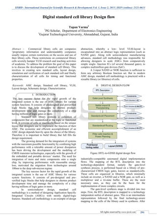
- 1. IJSRD - International Journal for Scientific Research & Development| Vol. 1, Issue 2, 2013 | ISSN (online): 2321-0613 All rights reserved by www.ijsrd.com Digital standard cell library Design flow Tapan Varma1 1 PG Scholar, Department of Electronics Engineering 1 Gujarat Technological University, Ahmadabad, Gujarat, India Abstract – Commercial library cells are companies ‘proprietary information and understandably companies usually impose certain restrictions on the access and use of their library cells. Those restrictions on commercial library cells severely hamper VLSI research and teaching activities of academia. To address the problem the goal of this paper is to discuss the development of standard cell library. This involves in creating new standard cells, layout design, simulation and verification of each standard cell and finally characterization of all cells for timing and functional properties. Keywords: ASIC design, Standard cell library, VLSI, Layout design, Schematic design, Characterization. I. INTRODUCTION The key success factor for the rapid growth of the integrated system is the use of ASIC library for various system functions. It consists of predesigned and preverified logic blocks that help designers to shorten product- development time and manage the complexity of a chip having millions of logic gates or more. Standard cell library contains a collection of components that are standardized at the logic or functional level. It consists of cells or macrocells based on the unique layout that designers use to implement the function of their ASIC. The economic and efficient accomplishment of an ASIC design depends heavily upon the choice of the library. Therefore it is important to build library that full fills the design requirement. The growing demand for the integration of systems with the maximum possible functionality by combining high performance with a tolerable amount of power dissipation has been driving the development and the modeling of CMOS transistor technologies, especially with the growth of the embedded and portable devices’ market. The need for integration of more and more components onto a single chip, by improving performance with reasonable energy loss, motivated the migration from technologies around 100nm to the deep sub-micron regime. The key success factor for the rapid growth of the integrated system is the use of ASIC library for various system functions. It consists of pre-designed and pre- verified logic blocks that help designers to shorten product development time and manage the complexity of a chip having millions of logic gates or more. In semiconductor design, standard cell methodology is a method of designing Application Specific Integrated Circuits (ASICs) with mostly digital-logic features. Standard cell methodology is an example of design abstraction, whereby a low- level VLSI-layout is encapsulated into an abstract logic representation (such as NAND gate). Along with semiconductor manufacturing advances, standard cell methodology was responsible for allowing designers to scale ASICs from comparatively simple single- function ICs (of several thousand gates), to complex multimillion gate devices (SoC). A 2-input NAND or NOR function is sufficient to form any arbitrary Boolean function set. But in modern ASIC design, standard cell methodology is practiced with a sizeable library (or libraries) of cells. II. DIGITAL DESIGN FLOW Figure.1RTL-to-GDSII digital design flow industrially-compatible automated digital implementation flows. The mapping of the RTL description into the technology-dependent format, namely the gate-level synthesis process, is performed based on a library of pre- characterized CMOS logic gates, known as standard-cells. These cells are organized in libraries, which minimally include an inverter, a NAND and a NOR gate, as well as a multiplexer and a tri-state buffer. These are the most necessary ones, as they can be the basis for the implementation of more complex circuits. The gate-level synthesis stage is divided into two steps. First, the RTL description is mapped to a technology independent netlist of abstract gates. This is an intermediate representation followed by the final technology-aware mapping to the cells of the library used in synthesis. After
- 2. Digital Standard Battery Design flow (IJSRD/Vol. 1/Issue 2/2013/00 ) All rights reserved by www.ijsrd.com this mapping step, the synthesizer optimizes the design, considering the timing, area and power constraints given by the designer, as long as the available cells of the library. Therefore, the synthesis tool should be aware of the cells’ timing, area and power characteristics. Hence, the standard cells should have been already characterized in terms of performance, area and power dissipation, to enable the synthesis tool’s optimizations. Characterization implies that the transistor-level netlists of these cells should be fed to an analog simulator with various input slews and output load capacitances, as well as the operating conditions of voltage and temperature, and simulated. The result of this process is the timing, power and area characteristics for each library’s cell, at the specific design corner and operating conditions. These metrics are written in a different file format adopted by different tools. (Generally written in a LIB file) The LIB file is also used at the physical implementation stage, which follows synthesis. At this stage, the place-and-route tools should be aware of the geometry of cells and interconnects, as well as of design rules like the minimum inter-metal spacing, given the technology. This information is extracted from the physical design (layout) of cells. The place-and-route tools need information about the width and height of cells, as well as the location and the dimensions of their input and output pins. The cell layouts are driven to the Abstract Generator, which produces the Library Exchange Format (LEF) file, which contains this information. In addition to the above, LEF files provide information about the technology’s metal stack and the minimum width, spacing and thickness of the available layers. The successful completion of placement and routing is followed by the post-layout simulation step, which verifies the design’s functionality. This step requires the information about the functionality of standard-cells, comprising the post layout netlist. This information is produced at the characterization and it is written to a Verilog file, which includes the gate level netlist of each cell, along with the input-to- output delay of each path. In the RTL-to-GDSII flow of Fig. 1, the LIB is used for timing and power analysis at both the post- synthesis and the post-layout steps. The information in the LEF file determines placement and routing, by providing the cell and interconnects physical dimensions and the design rules regarding wires and VIAS these two files comprise the core of a standard- cell library. A standard-cell library generation suite should minimally produce both of them, along with the gate-level netlist of cells, which is given usually in Verilog and it is required for the post-synthesis and the post-layout simulation of designs built with the specific standard-cell library. III. STANDARD CELL DESIGN FLOW Schematic DesignA. The Figure.2 shows the design flow for the standard cell. The design starts with the circuit topology of the cell either using schematic or netlist entry. At this stage, the width of NMOS Wn and PMOS Wp, of the transistor are optimized. Wp and Wn are selected to meet design specifications such as power dissipation, propagation delay, noise immunity and area. The value of Wp and Wn are determined by: DC switching point, which is approximately 50% of the Vdd. Driving capability of the cell, i.e. the number of fan out that the cell can drive. For an approximate same rise and fall time, Wp is normally three times wider than Wn. A circuit simulator is used to determine the switching point. Figure.2 The flow chart for standard cell design Layout Methdology If the circuit functions as expected, the physical design for the cell will be created and the parasitic value such as capacitance is back- annotated to obtain the actual delay associated with the interconnect. The layout uses the standard cell technique, where signals are routed in polysilicon perpendicular to the power. This approach result in a dense layout for CMOS gates, as the vertical polysilicon wire can serve as the input to both the NMOS and PMOS transistor. The row of NMOS and PMOS transistor is separated by a distance specified in the design rule separation between n and p active area. Power and ground busses traverse the cell at the top and bottom respectively. The internal area of the cell is used for routing the MOSFET of specific gates. To complete the logic gate, connections is made in metal, where metal1 routed horizontally and metal2 vertically. Characterization Process 1) Introduction The cells are simulated to ensure proper functionality and timing. The results from the initial design and extracted values are compared. There are many models which we can use to simulate the nominal process from the fabrication. Measurements of all delay times are at 50% to 50% Vdd values. All rise/fall times are 20% to 80% Vdd values. To obtain realistic manufacturing process characteristic, circuit simulation is performed with temperature, voltage and process parameter over the range of values that are expected to occur. The critical values at process comer are simulated with minimum and maximum condition.
- 3. Digital Standard Battery Design flow (IJSRD/Vol. 1/Issue 2/2013/00 ) All rights reserved by www.ijsrd.com 293 To exercise all input-to-output paths through the cells, input stimulus will be provided to the circuit simulator. Since many repetitive executions of the circuit simulator are required for each cell, the characterization is done using an automatic cell characterization tool. 2) Characterization Flow The characterization flow for std. cell is a major issue. Many aspects of the characterization demand special attention. The major steps are given below Netlist Extraction: In this, the layout for the cell to be characterized is made using any good layout editor for a specific technology & then verified for the technology rules violations & interconnections. After verifying the design, the parasitic extraction is done in which resistance; capacitance & other physical parasitic are being extracted from the design. Figure.3 characterization flow Specification of Parameters: After the extraction, some default, process & design dependent parameters are defined. For example, doping density, voltage, temperature, Fan out etc. Model Selection and Specification: After specifying the parameter values, different models are selected depending on their accuracy, complexity & requirement. A Model estimates the timing, area, power & noise parameters of the std. cell. In real sense, Models are mathematical equations used to calculate the o/p parameters. Measurement: The output provided by the simulator is then measured to extract the required characterization parameters. The output may be in different forms e.g. graphical view, bar chart and shmoo plot etc. From these characteristics, different parameters like area, power and timing are calculated for the std. cell. Model Generation: Using these parameters, a characterized o/p model for the std. cell is prepared in a format to which a design tool can understand. All the measured parameters are attached to std. cell. Verification: After the characterization of the std. cell, it is verified for different parameters by building a design from it. If it gives the desired result then the library is sign out. But if there is any error then flow is repeated from different stages depending on the severity of the error. MODEL DEVELOPMENT AND DOCUMENTATION After characterizing, the cells functional description and timing data are transformed to the format required by a specific design tools. Most design tools utilize special- purpose model formats with syntax for explicitly describing propagation delays, timing checks, and other aspects of cell behavior that are required by the tool. The final requirement is a documentation that summaries the functionality and timing of each cell. The functionality is frequently described with truth table, and timing data is presented in a simple format in the datasheet. The documentation for each library contains: setup and hold times Minimum cycle time, enable and disable time truth table for small/medium complexity cells operating range of temperature and voltage fan-in and fan-out variation of timing due to temperature and voltage path delays library cell symbol Timing diagrams. IV. CONCLUSION As new technology arrives, IC design and manufacturing activities become more complex. In such environment, a successful design activity relies heavily on the ASIC library. The advantages of having library are faster time-tomarket and reuse of often complex logic functions. The design methodology and requirement has been described. It is obvious that a very careful procedure and format has to be followed in order to produce a good cell library for ASIC design. Finally, modeling the silicon into the EDA tools play an important role to achieve accurate timing characteristic for the library, thus guarantee a working final product. Digital standard cell library is very useful in ASIC design. Standard library cells improve designers’ productivity through reduced design time and debugging. Implementing this flow using CAD tools available in market, you can design standard cell library. ACKNOWLEDGEMENT The authors would like to express their appreciation to the Gujarat Technological University, Department of Electronics Engineering for their kind. The authors also would like to thanks the Seer Akademi Institute for giving continuous guidance throughout the project. REFERANCES [1] Bekiaris, D., “A standard-cell library suite for deep-deep sub-micron CMOS technologies”, 2011, IEEE Conference Publications. Available: http://ieeexplore.ieee.org/ [2] “Development of TSMC 0.25μm Standard Cell Library” Available: http://www.vtvt.ece.vt.edu/ [3] Delay model information & difference between them. Available: http://www.deepchip.com/ [4] “Standard Cell Characterization” by: Richard Sohnius, Computer Architecture Group, University of Mannheim. Available: http://webserver.ziti.uni- heidelberg.de/ [5] Full Custom IC Design Flow Tutorial Using Synopsys Cosmos Tools Available: http://userwww.sfsu.edu/