A carbon nanotube (CNT) attached to the end of a conventional silicon (Si) atomic force microscope (AFM) tip enables scanning with higher spatial resolution and less tip wear than would otherwise be possible. The exceptional ease of use and mechanical stability of the NanoBot system make it possible to quickly accomplish this important nanofabrication task inside a scanning electron microscope (SEM).
Xidex manufactures and sells the NanoBot® system, an easy-to-use, highly versatile, user programmable nanomanipulator featuring specialized end-effectors for nanodevice fabrication and testing inside scanning electron microscopes (SEMs) and focused ion beam (FIB) tools.
Our mission is to enhance the R&D productivity of nanoscientists and nanotechnologists in both industry and academia. We offer best-in-class turnkey solutions to customers with well-defined requirements that are stable over time, and highly adaptable solutions to customers who need a system that can easily be augmented with additional plug-and-play nanopositioners and end-effectors as their needs evolve.
Unlocking the Power of ChatGPT and AI in Testing - A Real-World Look, present...
Xidex application note cnt afm tip fabrication using the nano bot system - 110313
1. Xidex Carbon Nanotube AFM Tip Fabrication
Using the NanoBot® System
Application Note
Vladimir Mancevski
Xidex Corporation
Introduction
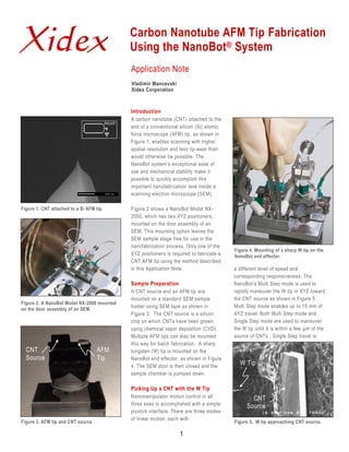
A carbon nanotube (CNT) attached to the
end of a conventional silicon (Si) atomic
force microscope (AFM) tip, as shown in
Figure 1, enables scanning with higher
spatial resolution and less tip wear than
would otherwise be possible. The
NanoBot system’s exceptional ease of
use and mechanical stability make it
possible to quickly accomplish this
important nanofabrication task inside a
500 nm scanning electron microscope (SEM).
500 nm
Figure 1. CNT attached to a Si AFM tip. Figure 2 shows a NanoBot Model NX-
2000, which has two XYZ positioners,
mounted on the door assembly of an
SEM. This mounting option leaves the
SEM sample stage free for use in the
nanofabrication process. Only one of the
Figure 4. Mounting of a sharp W tip on the
XYZ positioners is required to fabricate a NanoBot end effector.
CNT AFM tip using the method described
in this Application Note. a different level of speed and
corresponding responsiveness. The
Sample Preparation NanoBot’s Multi Step mode is used to
A CNT source and an AFM tip are rapidly maneuver the W tip in XYZ toward
mounted on a standard SEM sample the CNT source as shown in Figure 5.
Figure 2. A NanoBot Model NX-2000 mounted
holder using SEM tape as shown in Multi Step mode enables up to 15 mm of
on the door assembly of an SEM.
Figure 3. The CNT source is a silicon XYZ travel. Both Multi Step mode and
chip on which CNTs have been grown Single Step mode are used to maneuver
using chemical vapor deposition (CVD). the W tip until it is within a few µm of the
Multiple AFM tips can also be mounted source of CNTs. Single Step travel is
this way for batch fabrication. A sharp
CNT AFM tungsten (W) tip is mounted on the
Source Tip NanoBot end effector, as shown in Figure
4. The SEM door is then closed and the W Tip
sample chamber is pumped down.
Picking Up a CNT with the W Tip
Nanomanipulator motion control in all CNT
three axes is accomplished with a simple Source
joystick interface. There are three modes
of linear motion, each with
Figure 3. AFM tip and CNT source Figure 5. W tip approaching CNT source.
1
2. adjustable from 100 nm to 2 µm. The CNT source is then
examined by moving the SEM stage until a straight CNT is
found which is extending outward so that it can be easily W Tip
accessed as shown in Figure 6. This procedure typically
requires only a few minutes. The NanoBot system’s Fine CNT
Motion mode is then used to touch the W probe to the
selected CNT, as shown in Figure 7. The required high
degree of mechanical stability is enabled by the NanoBot
system’s extremely low drift, on the order of 10 nm per
minute, in all three axes. The Fine Motion mode enables ±
3.5 µm of motion with 1 nm resolution in XYZ. It normally
takes about 30 seconds to bring the W tip into well
oriented contact with a selected CNT. Next, the CNT is
welded to the W tip using electron beam induced
Figure 8. CNT separated from substrate using current pulse.
deposition (EBID) of carbon.
Attaching the CNT to the AFM Tip
The W tip carrying the CNT is rapidly translated in XYZ to
CNT within a few microns of the AFM tip apex, as shown in
Source Figure 9. The NanoBot system’s Fine Motion mode, is
then used to place the CNT along the side of the silicon
W Tip AFM tip apex, as shown in Figure 10.
CNT AFM Tip
W Tip
Figure 6. W tip maneuvered to within a few µm of a CNT.
CNT
Source
Figure 9. W tip carrying CNT translated to within a few
µm of the AFM tip.
CNT
W Tip AFM Tip
Figure 7. W tip in contact with the selected CNT.
CNT
W Tip
Separating the CNT from the CNT Source
An electrical current pulse is used to separate the CNT
from the CNT source substrate on which it was originally
grown, as shown in Figure 8. Figure 10. CNT placed along the side of the AFM tip.
2