
Recomendados
Más contenido relacionado
La actualidad más candente
La actualidad más candente (20)
Similar a Origianl Opto TLP781 P781 PC781 781 DIP-4 New
Similar a Origianl Opto TLP781 P781 PC781 781 DIP-4 New (20)
Más de AUTHELECTRONIC
Más de AUTHELECTRONIC (20)
Último
Último (20)
Origianl Opto TLP781 P781 PC781 781 DIP-4 New
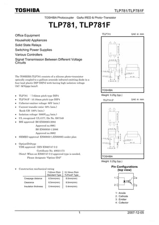
- 1. TLP781/TLP781F 2007-12-051 1 2 3 4 1 : Anode 2 : Cathode 3 : Emitter 4 : Collector TOSHIBA Photocoupler GaAs IRED & Photo−Transistor TLP781, TLP781F Office Equipment Household Appliances Solid State Relays Switching Power Supplies Various Controllers Signal Transmission Between Different Voltage Circuits The TOSHIBA TLP781 consists of a silicone photo−transistor optically coupled to a gallium arsenide infrared emitting diode in a four lead plastic DIP (DIP4) with having high isolation voltage (AC: 5kVRMS (min)). • TLP781 : 7.62mm pitch type DIP4 • TLP781F : 10.16mm pitch type DIP4 • Collector-emitter voltage: 80V (min.) • Current transfer ratio: 50% (min.) Rank GB: 100% (min.) • Isolation voltage: 5000Vrms (min.) • UL recognized: UL1577, file No. E67349 • BSI approved: BS EN60065:2002 Approved no.8961 BS EN60950-1:2006 Approved no.8962 • SEMKO approval: EN60950-1,EN60065 under plan • Option(D4)type VDE approved : DIN EN60747-5-2 Certificate No. 40021173 (Note): When an EN60747-5-2 approved type is needed, Please designate “Option (D4)” • Construction mechanical rating 7.62mm Pitch Standard Type 10.16mm Pitch TLPxxxF Type Creepage distance 6.5mm(min) 8.0mm(min) Clearance 6.5mm(min) 8.0mm(min) Insulation thickness 0.4mm(min) 0.4mm(min) Unit in mm TOSHIBA Weight: 0.25g (typ.) Unit in mm TOSHIBA Weight: 0.25g (typ.) Pin Configurations (top view) TLP781 TLP781F www.DataSheet.co.kr Datasheet pdf - http://www.DataSheet4U.net/
- 2. TLP781/TLP781F 2007-12-052 Current Transfer Ratio Current Transfer Ratio (%) (IC / IF) IF = 5mA, VCE = 5V, Ta = 25°C Type Classi− fication (Note 1) Min Max Marking Of Classification (None) 50 600 Blank, Y, Y+, YE,G, G+, B, B+,BL,GB Rank Y 50 150 YE Rank GR 100 300 GR Rank BL 200 600 BL Rank GB 100 600 GB Rank YH 75 150 Y+ Rank GRL 100 200 G Rank GRH 150 300 G+ TLP781 Rank BLL 200 400 B (Note 1): Ex. rank GB: TLP781 (GB) (Note 2): Application type name for certification test, please use standard product type name, i. e. TLP781 (GB): TLP781 Absolute Maximum Ratings (Ta = 25°C) Characteristic Symbol Rating Unit Forward current IF 60 mA Forward current derating(Ta ≥ 39°C) ΔIF / °C −0.7 mA / °C Pulse forward current (Note 3) IFP 1 A Power dissipation PD 100 mW Power dissipation derating ΔPD / °C −1.0 mW / °C Reverse voltage VR 5 V LED Junction temperature Tj 125 °C Collector−emitter voltage VCEO 80 V Emitter−collector voltage VECO 7 V Collector current IC 50 mA Power dissipation(single circuit) PC 150 mW Power dissipation derating (Ta ≥ 25°C)(single circuit) ΔPC / °C −1.5 mW / °C Detector Junction temperature Tj 125 °C Operating temperature range Topr −55~110 °C Storage temperature range Tstg −55~125 °C Lead soldering temperature (10s) Tsol 260 °C Total package power dissipation PT 250 mW Total package power dissipation derating (Ta ≥ 25°C) ΔPT / °C −2.5 mW / °C Isolation voltage (Note 4) BVS 5000 Vrms (Note): Using continuously under heavy loads (e.g. the application of high temperature/current/voltage and the significant change in temperature, etc.) may cause this product to decrease in the reliability significantly even if the operating conditions (i.e. operating temperature/current/voltage, etc.) are within the absolute maximum ratings. Please design the appropriate reliability upon reviewing the Toshiba Semiconductor Reliability Handbook (“Handling Precautions”/“Derating Concept and Methods”) and individual reliability data (i.e. reliability test report and estimated failure rate, etc). (Note 3): 100μs pulse, 100Hz frequency (Note 4): AC, 1 min., R.H.≤ 60%. Apply voltage to LED pin and detector pin together. www.DataSheet.co.kr Datasheet pdf - http://www.DataSheet4U.net/
- 3. TLP781/TLP781F 2007-12-053 Recommended Operating Conditions Characteristic Symbol Min Typ. Max Unit Supply voltage VCC ― 5 24 V Forward current IF ― 16 25 mA Collector current IC ― 1 10 mA Operating temperature Topr −25 ― 85 °C (Note): Recommended operating conditions are given as a design guideline to obtain expected performance of the device. Additionally, each item is an independent guideline respectively. In developing designs using this product, please confirm specified characteristics shown in this document. Individual Electrical Characteristics (Ta = 25°C) Characteristic Symbol Test Condition Min Typ. Max Unit Forward voltage VF IF = 10 mA 1.0 1.15 1.3 V Reverse current IR VR = 5 V ― ― 10 μA LED Capacitance CT V = 0, f = 1 MHz ― 30 ― pF Collector−emitter breakdown voltage V(BR) CEO IC = 0.5 mA 80 ― ― V Emitter−collector breakdown voltage V(BR) ECO IE = 0.1 mA 7 ― ― V VCE = 24 V ― 0.01 0.1 μA Collector dark current ID(ICEO) VCE = 24 V Ta = 85°C ― 0.6 50 μA Detector Capacitance (collector to emitter) CCE V = 0, f = 1 MHz ― 10 ― pF Coupled Electrical Characteristics (Ta = 25°C) Characteristic Symbol Test Condition Min Typ. Max Unit 50 ― 600 Current transfer ratio IC / IF IF = 5 mA, VCE = 5 V Rank GB 100 ― 600 % ― 60 ― Saturated CTR IC / IF (sat) IF = 1 mA, VCE = 0.4 V Rank GB 30 ― ― % IC = 2.4 mA, IF = 8 mA ― ― 0.4 ― 0.2 ― Collector−emitter saturation voltage VCE (sat) IC = 0.2 mA, IF = 1 mA Rank GB ― ― 0.4 V Isolation Characteristics (Ta = 25°C) Characteristic Symbol Test Condition Min Typ. Max Unit Capacitance (input to output) CS VS = 0, f = 1 MHz ― 0.8 ― pF Isolation resistance RS VS = 500 V 1×10 12 10 14 ― Ω AC, 1 minute 5000 ― ― AC, 1 second, in oil ― 10000 ― Vrms Isolation voltage BVS DC, 1 minute, in oil ― 10000 ― Vdc www.DataSheet.co.kr Datasheet pdf - http://www.DataSheet4U.net/
- 4. TLP781/TLP781F 2007-12-054 Switching Characteristics (Ta = 25°C) Characteristics Symbol Test Condition Min Typ. Max Unit Rise time tr ― 2 ― Fall time tf ― 3 ― Turn−on time ton ― 3 ― Turn−off time toff VCC = 10 V, IC = 2 mA RL = 100Ω ― 3 ― μs Turn−on time tON ― 2 ― Storage time ts ― 25 ― Turn−off time tOFF RL = 1.9 kΩ (Note 5) VCC = 5 V, IF = 16 mA ― 50 ― μs Surface-Mount Lead Form Options TOSHIBA ― Weight : 0.24g (typ.) TOSHIBA ― Weight : 0.24g (typ.) (Note 5): Switching time test circuit IF VCE VCC tON 4.5V 0.5V tOFF ts VCC VCE IF RL Unit in mm Unit in mmTLP781F(LF7)TLP781(LF6) www.DataSheet.co.kr Datasheet pdf - http://www.DataSheet4U.net/
- 5. TLP781/TLP781F 2007-12-055 Specifications for Embossed-Tape Packing: (TP6), (TP7) 1. Applicable Package Package Name Product Type DIP4LF6 TLP781 DIP4LF7 TLP781F 2. Product Naming System Type of package used for shipment is denoted by a symbol suffix after a product number. The method of classification is as below. (Example 1) TLP781(BL-TP6) Tape type CTR rank Device name (Example 2) TLP781F(BL-TP7) Tape type CTR rank Device name 3. Tape Dimensions 3.1 Orientation of Device in Relation to Direction of Tape Movement Device orientation in the recesses is as shown in Figure 1. Figure1 Device Orientation 3.2 Tape Packing Quantity:2000 devices per reel 3.3 Empty Device Recesses Are as Shown in Table 1. Table1 Empty Device Recesses Standard Remarks Occurrences of 2 or more successive empty device recesses 0 Within any given 40-mm section of tape, not including leader and trailer Single empty device recesses 6 devices (max.) per reel Not including leader and trailer 3.4 Start and End of Tape The start of the tape has 30 or more empty holes. The end of the tape has 50 or more empty holes. Tape feed www.DataSheet.co.kr Datasheet pdf - http://www.DataSheet4U.net/
- 6. TLP781/TLP781F 2007-12-056 3.5 Tape Specification [1] TLP781 (TP6) (1)Tape material: Plastic (2)Dimensions: The tape dimensions are as shown in Figure 2. Figure 2 Tape Forms [2] TLP781F (TP7) (1)Tape material: Plastic (2)Dimensions: The tape dimensions are as shown in Figure 3. Figure 3 Tape Forms 7.5±0.1 0.33±0.02 4.45±0.1 10.6±0.1 4.2±0.1 1.75±0.1 8.0±0.1 4.0±0.1 2.0±0.1 φ1.5 +0.2 -0 φ1.5 +0.1 -0 16.0 +0.2 -0.1 11.5±0.10.33±0.02 5.05±0.1 12.35±0.1 24.0 4.4±0.1 1.75±0.1 8.0±0.1 4.0±0.1 2.0±0.1 φ1.5 +0.1 -0 +0.3 -0.1 φ1.5+0.25 -0 www.DataSheet.co.kr Datasheet pdf - http://www.DataSheet4U.net/
- 7. TLP781/TLP781F 2007-12-057 3.6 Reel Specification [1] TLP781 (TP6) (1)Material: Plastic (2)Dimensions: The reel dimensions are as shown in Figure 4. Figure 4 Reel Forms [2] TLP781F (TP7) (1)Material: Plastic (2)Dimensions: The reel dimensions are as shown in Figure 5. Figure 5 Reel Forms 4. Packing One reel of photocouplers is packed in a shipping carton. 5. Label Indication The carton bears a label indicating the product number, the symbol representing classification of standard, the quantity, the lot number and the Toshiba company name. 6. Ordering Information When placing an order, please specify the product number, the CTR rank, the tape type and the quantity as shown in the following example. (Example) TLP781(BL-TP6)2000Pcs. Quantity (must be a multiple of 2000) Tape type CTR rank Device name (Note): The order code may be suffixed with wither a letter or a digit. Please contact your nearest Toshiba sales representative for more details. 16.4 23max φ332max φ102±1.5 φ13.0±0.5 3.6±0.8 1.5±0.5 +2.0 -0 Unit: mm φ330max φ100±1.5 φ13.0±0.5 31max 1.9±0.5 4.0±0.3 24.4 +2.0 -0 www.DataSheet.co.kr Datasheet pdf - http://www.DataSheet4U.net/
- 8. TLP781/TLP781F 2007-12-058 Soldering and Storage 1. Soldering 1.1 Soldering When using a soldering iron or medium infrared ray/hot air reflow, avoid a rise in device temperature as much as possible by observing the following conditions. 1) Using solder reflow ·Temperature profile example of lead (Pb) solder ·Temperature profile example of using lead (Pb)-free solder 2) Using solder flow (for lead (Pb) solder, or lead (Pb)-free solder) ・Please preheat it at 150°C between 60 and 120 seconds. ・Complete soldering within 10 seconds below 260°C. Each pin may be heated at most once. 3) Using a soldering iron Complete soldering within 10 seconds below 260°C, or within 3 seconds at 350°C. Each pin may be heated at most once. Time (s) (°C) 240 210 160 60~120s less than 30s Packagesurfacetemperature 140 Time (s) (°C) 260 230 190 60~120s 30~50s 180 Packagesurfacetemperature This profile is based on the device’s maximum heat resistance guaranteed value. Set the preheat temperature/heating temperature to the optimum temperature corresponding to the solder paste type used by the customer within the described profile. This profile is based on the device’s maximum heat resistance guaranteed value. Set the preheat temperature/heating temperature to the optimum temperature corresponding to the solder paste type used by the customer within the described profile. www.DataSheet.co.kr Datasheet pdf - http://www.DataSheet4U.net/
- 9. TLP781/TLP781F 2007-12-059 2. Storage 1) Avoid storage locations where devices may be exposed to moisture or direct sunlight. 2) Follow the precautions printed on the packing label of the device for transportation and storage. 3) Keep the storage location temperature and humidity within a range of 5°C to 35°C and 45% to 75%, respectively. 4) Do not store the products in locations with poisonous gases (especially corrosive gases) or in dusty conditions. 5) Store the products in locations with minimal temperature fluctuations. Rapid temperature changes during storage can cause condensation, resulting in lead oxidation or corrosion, which will deteriorate the solderability of the leads. 6) When restoring devices after removal from their packing, use anti-static containers. 7) Do not allow loads to be applied directly to devices while they are in storage. 8) If devices have been stored for more than two years under normal storage conditions, it is recommended that you check the leads for ease of soldering prior to use. www.DataSheet.co.kr Datasheet pdf - http://www.DataSheet4U.net/
- 10. TLP781/TLP781F 2007-12-0510 EN60747 Isolation Characteristics Types: TLP781, TLP781F Type designations for ‘option: (D4) ’, which are tested under EN60747 requirements. Ex.: TLP781 (D4-GR-LF6) D4: EN60747 option GR: CTR rank name LF6: standard lead bend name Note: Use TOSHIBA standard type number for safety standard application. Ex. TLP781 (D4-GR-LF6) → TLP781 Description Symbol Rating Unit Application classification for rated mains voltage ≤ 300 Vrms for rated mains voltage ≤ 600 Vrms I−IV I−III ― Climatic classification 55 / 115 / 21 ― Pollution degree 2 ― Maximum operating insulation voltage VIORM 890 Vpk Input to output test voltage, Vpr = 1.5×VIORM, type and sample test tp = 10s, partial discharge < 5pC Vpr 1335 Vpk Input to output test voltage, Vpr = 1.875×VIORM, 100% production test tp = 1s, partial discharge < 5pC Vpr 1670 Vpk Highest permissible overvoltage (transient overvoltage, tpr = 60s) VTR 6000 Vpk Safety limiting values (max. permissible ratings in case of fault) current (input current IF, Psi = 0) power (output or total power dissipation) temperature Isi Psi Tsi 300 500 150 mA mW °C Insulation resistance, VIO = 500V,Ta=25℃ Rsi ≧10 12 Ω www.DataSheet.co.kr Datasheet pdf - http://www.DataSheet4U.net/
- 11. TLP781/TLP781F 2007-12-0511 Insulation Related Specifications 7.62mm pitch TLPxxx type 10.16mm pitch TLPxxxF type Minimum creepage distance Cr 6.5mm 8.0mm Minimum clearance Cl 6.5mm 8.0mm Minimum insulation thickness ti 0.4 mm Comparative tracking index CTI 175 (1) If a printed circuit is incorporated, the creepage distance and clearance may be reduced below this value. (e.g.at a standard distance between soldering eye centres of 7.5mm). If this is not permissible, the user shall take suitable measures. (2) This photocoupler is suitable for ‘safe electrical isolation’ only within the safety limit data. Maintenance of the safety data shall be ensured by means of protective circuits. VDE test sign: Marking on product for EN60747 Marking on packing for EN60747 Marking Example: TLP781, TLP781F 4 CTR Rank Marking Lot No. Device Name 4: Mark for option (D4) 1pin indication P www.DataSheet.co.kr Datasheet pdf - http://www.DataSheet4U.net/
- 12. TLP781/TLP781F 2007-12-0512 1 10 100 1000 0.00 0.40 0.80 1.20 1.60 2.00 2.40 IFP – VFP PulseforwardcurrentIFP(mA) Pulse forward voltage VFP (V) 0.1 1.0 10.0 100.0 0.40 0.60 0.80 1.00 1.20 1.40 1.60 0 20 40 60 80 100 -20 0 20 40 60 80 100 120 IF – Ta Allowableforwardcurrent IF(mA) Ambient temperature Ta (℃) 120 PC – Ta Allowablecollectorpower dissipationPC(mW) Ambient temperature Ta (℃) 200 100 160 806020 400−20 0 120 80 40 IF – VF ForwardcurrentIF(mA) Forward voltage VF (V) Pulse width ≤ 10μs Repetitive frequency=100Hz Ta = 25℃ -3.0 -2.6 -2.2 -1.8 -1.4 -1.0 -0.6 0 1 10 100 Forwardvoltagetemperature coefficientΔVF/ΔTa(mV/℃) ΔVF / ΔTa – IF Forward current IF (mA) 0.1 *: The above graphs show typical characteristics. www.DataSheet.co.kr Datasheet pdf - http://www.DataSheet4U.net/
- 13. TLP781/TLP781F 2007-12-0513 0 10 20 30 0.0 0.2 0.4 0.6 0.8 1.0 1.2 0.01 0.10 1.00 10.00 100.00 0.1 1 10 100 1 10 100 1000 0.1 1 10 100 Collector-emitter voltage VCE (V) CollectorcurrentIC(mA) IC – VCE 0 20 40 60 80 0 2 4 6 8 10 0.0001 0.001 0.01 0.1 1 10 0 20 40 60 80 100 Collector-emitter voltage VCE (V) CollectorcurrentIC(mA) IC – VCE IC – IF CollectorcurrentIC(mA) Forward current IF (mA) Ta = 25°C VCE = 5V VCE = 0.4V IC /IF – IF CurrenttransferratioIC/IF(%) Ta = 25°C VCE = 5V VCE = 0.4V ID – Ta Ambient temperature Ta (℃) CollectordarkcurrentIC(μA) 50 10 20 5 IF= 2 mA 30 15 50 10 20 5 IF= 2 mA 30 15 Forward current IF (mA) *: The above graphs show typical characteristics. www.DataSheet.co.kr Datasheet pdf - http://www.DataSheet4U.net/
- 14. TLP781/TLP781F 2007-12-0514 0.00 0.04 0.08 0.12 0.16 0.20 -40 -20 0 20 40 60 80 100 0 1 10 100 -40 -20 0 20 40 60 80 100 1 10 100 1000 1 10 100 Ambient temperature Ta (℃) Collector-emittersaturation voltageVCE(sat)(V) VCE(sat) – Ta Switching Time – RL Switchingtime(μs) Load resistance RL (kΩ) tON Ta = 25°C IF = 16mA VCC = 5V tOFF tS IF = 5 mA IC = 1 mA Ambient temperature Ta (℃) CollectorcurrentIC(mA) IC – Ta VCE = 5V IF= 0.5 mA 1mA 5mA 10mA 20mA 0.1 *: The above graphs show typical characteristics. www.DataSheet.co.kr Datasheet pdf - http://www.DataSheet4U.net/
- 15. TLP781/TLP781F 2007-12-0515 RESTRICTIONS ON PRODUCT USE 20070701-EN • The information contained herein is subject to change without notice. • TOSHIBA is continually working to improve the quality and reliability of its products. Nevertheless, semiconductor devices in general can malfunction or fail due to their inherent electrical sensitivity and vulnerability to physical stress. It is the responsibility of the buyer, when utilizing TOSHIBA products, to comply with the standards of safety in making a safe design for the entire system, and to avoid situations in which a malfunction or failure of such TOSHIBA products could cause loss of human life, bodily injury or damage to property. In developing your designs, please ensure that TOSHIBA products are used within specified operating ranges as set forth in the most recent TOSHIBA products specifications. Also, please keep in mind the precautions and conditions set forth in the “Handling Guide for Semiconductor Devices,” or “TOSHIBA Semiconductor Reliability Handbook” etc. • The TOSHIBA products listed in this document are intended for usage in general electronics applications (computer, personal equipment, office equipment, measuring equipment, industrial robotics, domestic appliances, etc.).These TOSHIBA products are neither intended nor warranted for usage in equipment that requires extraordinarily high quality and/or reliability or a malfunction or failure of which may cause loss of human life or bodily injury (“Unintended Usage”). Unintended Usage include atomic energy control instruments, airplane or spaceship instruments, transportation instruments, traffic signal instruments, combustion control instruments, medical instruments, all types of safety devices, etc.. Unintended Usage of TOSHIBA products listed in his document shall be made at the customer’s own risk. • The products described in this document shall not be used or embedded to any downstream products of which manufacture, use and/or sale are prohibited under any applicable laws and regulations. • The information contained herein is presented only as a guide for the applications of our products. No responsibility is assumed by TOSHIBA for any infringements of patents or other rights of the third parties which may result from its use. No license is granted by implication or otherwise under any patents or other rights of TOSHIBA or the third parties. • GaAs(Gallium Arsenide) is used in this product. The dust or vapor is harmful to the human body. Do not break, cut, crush or dissolve chemically. • Please contact your sales representative for product-by-product details in this document regarding RoHS compatibility. Please use these products in this document in compliance with all applicable laws and regulations that regulate the inclusion or use of controlled substances. Toshiba assumes no liability for damage or losses occurring as a result of noncompliance with applicable laws and regulations. www.DataSheet.co.kr Datasheet pdf - http://www.DataSheet4U.net/