Original N-channel 600 V 0.160 Ω 19 A PowerFLAT™ 8x8 HV ultra low gate charge MDmesh™ II Power MOSFET STW26NM60 26NM60 26NM60N 600V 20A TO-247 New STMicroelectronics
This document provides information on the STL26NM60N N-channel 600 V, 0.160 Ω, 19 A PowerFLATTM 8x8 HV ultra low gate charge MDmeshTM II Power MOSFET, including:
- Key features such as being 100% avalanche tested and having low input capacitance and gate charge
- Applications in switching applications
- Description of the proprietary vertical and horizontal process technologies used to achieve extremely low on-resistance
- Electrical ratings, characteristics and switching performance curves
- Package mechanical data for the PowerFLATTM 8x8 HV package
Original MOSFET N-CHANNEL K15A60D K15A60U 15A60D 15A60 TO-220 15A 600V New
Similar a Original N-channel 600 V 0.160 Ω 19 A PowerFLAT™ 8x8 HV ultra low gate charge MDmesh™ II Power MOSFET STW26NM60 26NM60 26NM60N 600V 20A TO-247 New STMicroelectronics
Original Mosfet N 8N80C 8N80 FQPF8N80C FQPF8N80 8A 800V TO-220 New FairchildAUTHELECTRONIC
Similar a Original N-channel 600 V 0.160 Ω 19 A PowerFLAT™ 8x8 HV ultra low gate charge MDmesh™ II Power MOSFET STW26NM60 26NM60 26NM60N 600V 20A TO-247 New STMicroelectronics (20)
Original N-channel 600 V 0.160 Ω 19 A PowerFLAT™ 8x8 HV ultra low gate charge MDmesh™ II Power MOSFET STW26NM60 26NM60 26NM60N 600V 20A TO-247 New STMicroelectronics
1. November 2011 Doc ID 18472 Rev 2 1/14
14
STL26NM60N
N-channel 600 V, 0.160 Ω, 19 A PowerFLAT™ 8x8 HV
ultra low gate charge MDmesh™ II Power MOSFET
Features
■ 100% avalanche tested
■ Low input capacitance and gate charge
■ Low gate input resistance
Applications
■ Switching applications
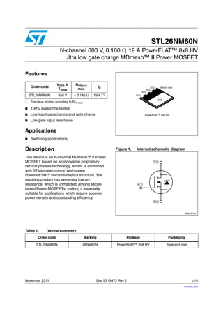
Description
This device is an N-channel MDmesh™ V Power
MOSFET based on an innovative proprietary
vertical process technology, which is combined
with STMicroelectronics’ well-known
PowerMESH™ horizontal layout structure. The
resulting product has extremely low on-
resistance, which is unmatched among silicon-
based Power MOSFETs, making it especially
suitable for applications which require superior
power density and outstanding efficiency.
Figure 1. Internal schematic diagram
Order code
VDSS @
TJmax
RDS(on)
max
ID
STL26NM60N 650 V < 0.185 Ω 19 A (1)
1. The value is rated according to Rthj-case
Table 1. Device summary
Order code Marking Package Packaging
STL26NM60N 26NM60N PowerFLAT™ 8x8 HV Tape and reel
www.st.com
3. STL26NM60N Electrical ratings
Doc ID 18472 Rev 2 3/14
1 Electrical ratings
Table 2. Absolute maximum ratings
Symbol Parameter Value Unit
VDS Drain-source voltage (VGS = 0) 600 V
VGS Gate-source voltage ± 25 V
ID
(1)
1. The value is rated according to Rthj-case
Drain current (continuous) at TC = 25 °C 19 A
ID
(1)
Drain current (continuous) at TC = 100 °C 12 A
ID
(2)
2. When mounted on FR-4 board of inch², 2oz Cu
Drain current (continuous) at Tamb = 25 °C 2.7 A
ID
(2)
Drain current (continuous) at Tamb = 100 °C 1.7 A
IDM
(2),(3)
Drain current (pulsed) 10.8 A
PTOT
(2) Total dissipation at Tamb = 25 °C 3 W
PTOT
(1)
Total dissipation at TC = 25 °C 125 W
IAR
Avalanche current, repetitive or not-
repetitive (pulse width limited by Tj max)
7.5 A
EAS
Single pulse avalanche energy
(starting Tj = 25 °C, ID = IAR, VDD = 50 V)
400 mJ
dv/dt (3)
3. ISD ≤ 19 A, di/dt ≤ 400 A/µs, VDS peak≤V(BR)DSS, VDD = 80% V(BR)DSS
Peak diode recovery voltage slope 15 V/ns
Tstg Storage temperature - 55 to 150 °C
Tj Max. operating junction temperature 150 °C
Table 3. Thermal data
Symbol Parameter Value Unit
Rthj-case Thermal resistance junction-case max 0.83 °C/W
Rthj-amb
(1)
1. When mounted on 1inch² FR-4 board, 2 oz Cu
Thermal resistance junction-amb max 45 °C/W
4. Electrical characteristics STL26NM60N
4/14 Doc ID 18472 Rev 2
2 Electrical characteristics
(TC = 25 °C unless otherwise specified)
Table 4. On /off states
Symbol Parameter Test conditions Min. Typ. Max. Unit
V(BR)DSS
Drain-source
breakdown voltage
ID = 1 mA, VGS = 0 600 V
IDSS
Zero gate voltage
drain current (VGS = 0)
VDS = 600 V
VDS =600 V, TC=125 °C
1
100
µA
µA
IGSS
Gate-body leakage
current (VDS = 0)
VGS = ± 25 V 100 nA
VGS(th) Gate threshold voltage VDS = VGS, ID = 250 µA 3 4 5 V
RDS(on)
Static drain-source on
resistance
VGS = 10 V, ID = 10 A 0.160 0.185 Ω
Table 5. Dynamic
Symbol Parameter Test conditions Min. Typ. Max. Unit
Ciss
Coss
Crss
Input capacitance
Output capacitance
Reverse transfer
capacitance
VDS = 50 V, f = 1 MHz,
VGS = 0
-
1800
115
1.1
-
pF
pF
pF
Coss(eq)
(1)
1. Coss eq. time related is defined as a constant equivalent capacitance giving the same charging time as Coss
when VDS increases from 0 to 80% VDSS
Equivalent
capacitance time
related
VDS = 0 to 480 V, VGS = 0 - 310 - pF
RG
Intrinsic gate
resistance
f = 1 MHz open drain - 2.8 - Ω
Qg
Qgs
Qgd
Total gate charge
Gate-source charge
Gate-drain charge
VDD = 480 V, ID = 19 A,
VGS = 10 V
(see Figure 14)
-
60
8.5
30
-
nC
nC
nC
5. STL26NM60N Electrical characteristics
Doc ID 18472 Rev 2 5/14
Table 6. Switching times
Symbol Parameter Test conditions Min. Typ. Max Unit
td(on)
tr
td(off)
tf
Turn-on delay time
Rise time
Turn-off delay time
Fall time
VDD = 300 V, ID = 10 A,
RG = 4.7 Ω, VGS = 10 V
(see Figure 15),
(see Figure 18)
-
13
25
85
50
-
ns
ns
ns
ns
Table 7. Source drain diode
Symbol Parameter Test conditions Min. Typ. Max. Unit
ISD
ISDM
(1)
1. Pulse width limited by safe operating area
Source-drain current
Source-drain current (pulsed)
-
19
76
A
A
VSD
(2)
2. Pulsed: pulse duration = 300 µs, duty cycle 1.5%
Forward on voltage ISD = 19 A, VGS = 0 - 1.5 V
trr
Qrr
IRRM
Reverse recovery time
Reverse recovery charge
Reverse recovery current
ISD = 19 A, di/dt = 100 A/µs
VDD = 100 V (see Figure 15)
-
370
5.8
31.5
ns
µC
A
trr
Qrr
IRRM
Reverse recovery time
Reverse recovery charge
Reverse recovery current
ISD = 19 A, di/dt = 100 A/µs
VDD = 100 V, Tj = 150 °C
(see Figure 15)
-
450
7.5
32.5
ns
µC
A
8. Test circuits STL26NM60N
8/14 Doc ID 18472 Rev 2
3 Test circuits
Figure 13. Switching times test circuit for
resistive load
Figure 14. Gate charge test circuit
Figure 15. Test circuit for inductive load
switching and diode recovery times
Figure 16. Unclamped inductive load test
circuit
Figure 17. Unclamped inductive waveform Figure 18. Switching time waveform
AM01468v1
VGS
PW
VD
RG
RL
D.U.T.
2200
μF
3.3
μF
VDD
AM01469v1
VDD
47kΩ
1kΩ
47kΩ
2.7kΩ
1kΩ
12V
Vi=20V=VGMAX
2200
μF
PW
IG=CONST
100Ω
100nF
D.U.T.
VG
AM01470v1
A
D
D.U.T.
S
B
G
25 Ω
A A
B
B
RG
G
FAST
DIODE
D
S
L=100μH
μF
3.3 1000
μF
VDD
AM01471v1
Vi
Pw
VD
ID
D.U.T.
L
2200
μF
3.3
μF VDD
AM01472v1
V(BR)DSS
VDDVDD
VD
IDM
ID
AM01473v1
VDS
ton
tdon tdoff
toff
tftr
90%
10%
10%
0
0
90%
90%
10%
VGS
9. STL26NM60N Package mechanical data
Doc ID 18472 Rev 2 9/14
4 Package mechanical data
In order to meet environmental requirements, ST offers these devices in different grades of
ECOPACK®
packages, depending on their level of environmental compliance. ECOPACK®
specifications, grade definitions and product status are available at: www.st.com. ECOPACK
is an ST trademark.
10. Package mechanical data STL26NM60N
10/14 Doc ID 18472 Rev 2
Table 8. PowerFLAT™ 8x8 HV mechanical data
Dim.
mm
Min. Typ. Max.
A 0.80 0.90 1.00
A1 0.00 0.02 0.05
b 0.95 1.00 1.05
D 8.00
E 8.00
D2 7.05 7.20 7.30
E2 4.15 4.30 4.40
e 2.00
L 0.40 0.50 0.60
aaa 0.10
bbb 0.10
ccc 0.10
11. STL26NM60N Package mechanical data
Doc ID 18472 Rev 2 11/14
Figure 19. PowerFLAT™ 8x8 HV drawing mechanical data
INDEX AREA
TOP VIEW
PLANE
SEATING
0.08 C
BOTTOM VIEW
SIDE VIEW
PIN#1 ID
D
E
b
A
E2
D2
L0.40
0.20±0.008
C
bbb C A B
BA
aaa C
aaa C
A1
ccc C
8222871_Rev_B
13. STL26NM60N Revision history
Doc ID 18472 Rev 2 13/14
5 Revision history
Table 9. Document revision history
Date Revision Changes
14-Feb-2011 1 First release.
03-Nov-2011 2
Section 4: Package mechanical data has been updated.
Minor text changes.