Más contenido relacionado
La actualidad más candente (20)
Similar a DS-00593-14-XTR70020-High-temperature, High Input Voltage, 2A Positive LDO Regulator (20)
DS-00593-14-XTR70020-High-temperature, High Input Voltage, 2A Positive LDO Regulator
- 1. XTRM Series
XTR70020
HIGH-TEMPERATURE, HIGH INPUT VOLTAGE, 2A POSITIVE
LDO REGULATOR
DS-00593-14 rev2F 2016-08-29 1 of 12
www.x-relsemi.com
© 2016 X-REL Semiconductor
FEATURES
▲Operational beyond the -60°C to +230°C temperature range.
▲Input voltages from 3.0V to 30V.
▲Possible output voltages from 0.6V to 30V.
▲Accurate bandgap reference (+/-3%).
▲No minimum dropout imposed (current limited).
▲High output current with low dropout:
o 1A @ 230°C with 0.63V, 2A @ 230°C with 1.4V
▲Low current consumption in full-power (2.3mA) and low-power
modes (950µA).
▲Over current protection (hiccup mode).
▲Customer selectable Thermal Shutdown protection.
▲Customer selectable UVLO protection.
▲Low noise : 550uV for Vout=15V / 75uV for Vout=0.9V
▲Soft startup and soft shutdown.
▲Stable over a wide range of load capacitance (0.5uF to 50µF).
▲Low temperature dependence (40 ppm/°C).
▲Excellent line (0.015%/V) and load (0.15%/A) regulations.
▲Monolithic design for high-reliability.
▲Latch-up free.
▲Ruggedized SMT and thru-hole packages.
▲Also available as bare die.
APPLICATIONS.
▲Reliability-critical, Automotive, Aeronautics & Aerospace,
Down-hole.
▲High-efficiency regulated power supplies, bridge excitation,
cable- or battery-powered applications.
DESCRIPTION
XTR70020 is a family of high-temperature, high-input voltage,
2Amp ultra low dropout voltage regulators designed for extreme
reliability high voltage and high temperature applications. Being
able to operate with input voltages from 3.0V to 30V, XTR70020
parts can source a current of 2A at +230°C while providing excel-
lent regulation characteristics with a dropout as low as 1.2V.
Several preset reference voltages are available from 0.6V to 15V
allowing output voltages from 0.6V to virtually 30V.
Four protection features are implemented to ensure a good oper-
ation and reliability of the circuit: UVLO, hiccup modes short-
circuit protection, customer selectable thermal shutdown, soft
turn-on/off.
XTR70020 parts can be used in a wide range of applications
such as high fan-out and low-dropout regulators, adjustable pow-
er supply, current sources, as well as precision bridge excitation.
Special design techniques were used allowing XTR70020 parts
to offer a precise, robust and reliable operation in critical applica-
tions. Full functionality is guaranteed from -60°C to +230°C,
though operation well below and above this temperature range is
achieved.
XTR70020 parts have been designed to reduce system cost and
ease adoption by reducing the learning curve and providing smart
and easy to use features.
Parts from the XTR70020 family are available in ruggedized SMT
and thru-hole packages, as well as bare dies.
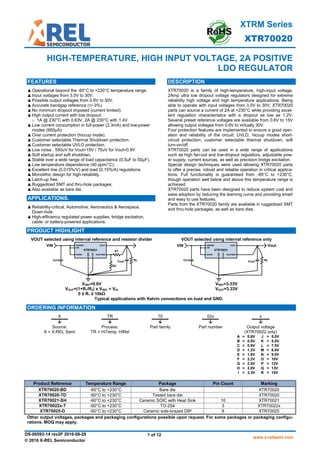
PRODUCT HIGHLIGHT
VOUT selected using internal reference and resistor divider VOUT selected using internal reference only
VREF=0.6V
VOUT=(1+R1/R2) x VREF < VIN
0 ≤ R1 ≤ 10kΩ
VREF=3.33V
VOUT=3.33V
Typical applications with Kelvin connections on load and GND.
ORDERING INFORMATION
X TR 70 02x x
Source:
X = X-REL Semi
Process:
TR = HiTemp, HiRel
Part family Part number Output voltage
(XTR70022 only)
A = 0.6V J = 5.0V
B = 0.8V K = 5.5V
C = 0.9V L = 7.5V
D = 1.2V M = 8.0V
E = 1.8V N = 9.0V
F = 2.2V O = 10V
G = 2.5V P = 12V
H = 2.8V Q = 13V
I = 3.3V R = 15V
Product Reference Temperature Range Package Pin Count Marking
XTR70020-BD -60°C to +230°C Bare die XTR70020
XTR70020-TD -60°C to +230°C Tested bare die XTR70020
XTR70021-SH -60°C to +230°C Ceramic SOIC with Heat Sink 10 XTR70021
XTR70022x-T -60°C to +230°C TO-254 3 XTR70022x
XTR70025-D -60°C to +230°C Ceramic side-brazed DIP 8 XTR70025
Other output voltages, packages and packaging configurations possible upon request. For some packages or packaging configu-
rations, MOQ may apply.
Cout
XTR70021
GND
VOUT
/SHDN VOUTSNS
Cin1 RL
R2
R1
VIN VINPWR
VIN
0.6V
Cout
XTR70021
GND
VOUT
/SHDN VOUTSNS
Cin1 RL
VIN
0.6V
VINPWR
VIN
Vout
- 2. XTR70020
DS-00593-14 rev2F 2016-08-29 2 of 12
www.x-relsemi.com
© 2016 X-REL Semiconductor
ABSOLUTE MAXIMUM RATINGS
Voltage on VIN, VINPWR and /SHDN to GND -0.5V to 35V
Voltage on any pin to GND -0.5V to VIN
Storage Temperature Range -60°C to +230°C
Operating Junction Temperature Range -60°C to +300°C
ESD Classification 1kV HBM MIL-STD-883
Caution: Stresses beyond those listed in “ABSOLUTE MAXIMUM RATINGS” may cause permanent damage to the device. These are
stress ratings only and functionality of the device at these or any other condition beyond those indicated in the operational sections of
the specifications is not implied. Exposure to “ABSOLUTE MAXIMUM RATINGS” conditions for extended periods may permanently
affect device reliability.
PRODUCT VARIANTS
CSOIC10 with Heat Sink
XTR70021-SH
TO-254
XTR70022x-T
Side-brazed DIP8
XTR70025-D
Top view
Heat sink (bottom of package)
connected to VIN
Front view Top view
1 VIN
2 GND
3 VOUT
BLOCK DIAGRAM
Different functionalities are available depending upon packaging configuration. Grey blocks represent the internal protections.
Arrows aside pad names indicate the input is internally pulled down. Contact X-REL for the Die and Assembly Specifications
document describing functionalities of all pads.
GND
0.6V
VOUT
VOUTSNS
1
2
3
4 VINPWR
VIN
VIN
/SHDN
8
7
65
9
10
VINPWRVOUT
21 3
GND
VOUT
VOUTSNS
1
2
3
4
VINPWR
VIN
/SHDN8
7
6
5 NCNC
3.33V
6.67V
2.2V
1.87V
1.67V
0.8V
0.6V
8V
/SHDN
GND(10V)
VOUT
XTR70020
Current-mode
Bandgap
Reference
VIN
VINPWR
VOUTSNS
Oscillator
Control
Logic
Soft Start
Soft Turn-off
Charge
Pump
UVLO
Over
Current
Protection
OCP
OCP
VIN
/TSEnbl
Thermal
Shutdown
VREF
/OCPEnbl
/VrefMult
/UVLOEnbl
1.5 VREF
Multiplier
- 3. XTR70020
DS-00593-14 rev2F 2016-08-29 3 of 12
www.x-relsemi.com
© 2016 X-REL Semiconductor
PADS DESCRIPTION
Pad Name Description
0.6V Connect to GND to set VREF=0.6V.
0.8V Connect to GND to set VREF=0.8V.
1.67V Connect to GND to set VREF=1.67V.
1.87V Connect to GND to set VREF=1.87V.
2.2V Connect to GND to set VREF=2.2V.
3.33V Connect to GND to set VREF=3.33V.
6.67V Connect to GND to set VREF=6.67V.
8V Connect to GND to set VREF=8V.
GND Circuit ground. If no “x.xV” pad connected, default VREF is 10V.
/SHDN
Active-low shutdown functionality. Connect to VIN to enable the circuit or to GND to disable it. Do not leave floating (no
internal pull).
/VrefMult
Multiplies the reference voltage selected by connecting any of xxV to GND by a factor of “3/2” (1.5). Left floating or con-
nect to VOUTSNS if not used. DO NEVER CONNECT to other terminals than GND or VOUTSNS.
VOUTSNS
Output voltage sense (Kelvin connection). It can be directly connected to VOUT or used to set the output voltage by
means of an external resistive divider.
VOUT Output voltage terminal. Decouple to GND with a capacitor of at least 10nF.
VINPWR Supply voltage of power transistor. Decouple to GND with a capacitor of at least 100nF.
VIN
Supply voltage of the internal blocks of the device. Connect directly to VINPWR pin or after a 10-100Ω / 10-100nF low-
pass filter.
/TSEnbl Active-low thermal shut-down enable. Internally pulled down.
/OCPEnbl Active-low over current protection enable. Internally pulled down.
/UVLOEnbl Active-low UVLO enable. Internally pulled down.
VREF SETTINGS
The following table is valid for the bare die of XTR70020 and assumes GND is connected to the 0V reference.
Voltage Selection Pads Connected to GND /VrefMult Connection Equivalent Reference Voltage
0.6V Floating 0.6V
0.6V GND 0.9V
0.8V Floating 0.8V
0.8V GND 1.2V
1.67V Floating 1.67V
1.67V GND 2.5V
1.87V Floating 1.87V
1.87V GND 2.8V
2.2V Floating 2.2V
2.2V GND 3.3V
3.33V Floating 3.33V
3.33V GND 5V
6.67V Floating 6.67V
6.67V GND 10V
8V Floating 8V
8V GND 12V
- Floating 10V
- GND 15V
When using the reference multiplier feature (/VrefMult is connected to GND) the maximum allowed R2 (see the “Basic Operation” section in
page 9) is 10kΩ.
- 4. XTR70020
DS-00593-14 rev2F 2016-08-29 4 of 12
www.x-relsemi.com
© 2016 X-REL Semiconductor
PIN DESCRIPTION
XTR70021-SH
Pin Number Name Description
1 GND Circuit ground.
2 0.6V Connect to GND to set VREF=0.6V.
3 VOUTSNS Output voltage sense. Must be connected close to the load.
4
VOUT Output voltage terminal. Decouple to GND with a capacitor of at least 500nF.
5
6
VINPWR Supply voltage terminal of power pass transistor.
7
8
VIN Supply voltage terminal.
9
10 /SHDN Active-low shut-down terminal. Connect to VIN when not used.
The default reference voltage (VREF) of XTR70021 is 3.33V. To change the reference voltage VREF to 0.6V, connect pin “0.6V” to GND. See
the “Basic Operation” section in page 9 for details on how to obtain any output voltage from the XTR70020 based on the internal settings
and external components.
Internal Settings of XTR70021-SH
Internal Pad Internal Setting Description
3.33V GND Default voltage set to 3.33V.
/VrefMult Floating Reference voltage multiplier disabled.
/TSEnbl VIN Thermal shut-down disabled.
/OCPEnbl GND Over-current (short-circuit) protection enabled.
/UVLOEnbl GND Under-voltage lockout (UVLO) enabled.
XTR70022x-T
Pin Number Name Description
1 VIN Supply voltage terminal.
2 GND Circuit ground.
3 VOUT Output voltage terminal. Decouple to GND with a capacitor of at least 500nF.
The output voltage (VOUT) of XTR70022 devices is set during the assembly of the parts. See the “Ordering Information” section to determine
the part number corresponding to the needed output voltage in your application.
Internal Settings of XTR70022x-T
Internal Pad Internal Setting Description
xxV GND Depends upon chosen part reference variant (A, B, C…).
/TSEnbl VIN Thermal shut-down disabled.
/OCPEnbl GND Over-current (short-circuit) protection enabled.
/UVLOEnbl GND Under-voltage lockout (UVLO) enabled.
- 5. XTR70020
DS-00593-14 rev2F 2016-08-29 5 of 12
www.x-relsemi.com
© 2016 X-REL Semiconductor
XTR70025-D
Pin Number Name Description
1 GND Circuit ground.
2 VOUTSNS Output voltage sense. Must be connected close to the load.
3 VOUT Output voltage terminal. Decouple to GND with a capacitor of at least 500nF.
4 N.C. No internal connection.
5 N.C. No internal connection.
6 VINPWR Supply voltage terminal of power pass transistor.
7 VIN Supply voltage terminal.
8 /SHDN Active-low shut-down terminal. Connect to VIN when not used.
The default reference voltage (VREF) of XTR70025 is 0.6V. See the “Basic Operation” section in page 9 for details on how to obtain any
output voltage from the XTR70020 based on the internal settings and external components.
Internal Settings of XTR70025-D
Internal Pad Internal Setting Description
0.6V GND Default reference voltage set to 0.6V.
/VrefMult Floating Reference voltage multiplier disabled.
/TSEnbl GND Thermal shut-down enabled.
/OCPEnbl GND Over-current (short-circuit) protection enabled.
/UVLOEnbl GND Under-voltage lockout (UVLO) enabled.
THERMAL CHARACTERISTICS
Parameter Condition Min Typ Max Units
XTR70021-SH
Thermal Resistance: J-C
RTh_J-C
Measured on ePAD. 4 °C/W
Thermal Resistance: J-A
RTh_J-A
ePAD thermally connected to 3cm² PCB copper. 70 °C/W
XTR70022-T
Thermal Resistance: J-C
RTh_J-C
Measure on back of package. 5 °C/W
Thermal Resistance: J-A
RTh_J-A
Still air. 50 °C/W
XTR70025-D
Thermal Resistance: J-C
RTh_J-C
25 °C/W
Thermal Resistance: J-A
RTh_J-A
100 °C/W
RECOMMENDED OPERATING CONDITIONS
Parameter Min Typ Max Units
Supply voltage
VIN
3.0 30 V
Load capacitance
CLoad
0.5 50 µF
Recommended input de-
coupling capacitor
Cdec
1 µF
Load current
ILoad
100µ 2 A
Junction Temperature1
Tj
-60 230 °C
1
Operation beyond the specified temperature range is achieved.
- 6. XTR70020
DS-00593-14 rev2F 2016-08-29 6 of 12
www.x-relsemi.com
© 2016 X-REL Semiconductor
ELECTRICAL SPECIFICATIONS
Unless otherwise stated, specification applies for VIN=VINPWR=20V, VREF=3.3V and VOUT=5V, -60°C<TC<230°C.
Parameter Condition Min Typ Max Units
Output Characteristics
Allowed Output Voltages
VOUT
3.0V≤VIN≤30V 0.6 VIN - 0.1 V
Maximum Output Current
IOUT_Max
XTR70020, XTR70021 and XTR70022
XTR70025 (Package limited)
2.0
0.7
A
Output Voltage Accuracy
VOUT/VOUT
IOUT=10mA and Tc=85°C -3 +3 %
Minimum Reference
Voltage Overhead1
VIN-VREF
3.0V≤VIN≤30V
0.9 1.1 V
Dropout Voltage
VIN-VOUT
IOUT=1A
TC=-60°C
TC=85°C
TC=230°C
0.23
0.41
0.63
V
Drift with Temperature2
1/VOUT.(VOUT/T)
0 40 100 ppm/°C
Line Regulation2
1/VOUT.(VOUT/VhIN)
ILOAD = 1mA at Tc=230°C (worst case)
VIN from MAX[3V; VOUT+1V] to 24V
VIN from 24V to 30V
0.015
0.08
0.06
0.3
%/V
Load regulation
1/VOUT.(VOUT/ILOAD)
ILOAD from 1mA to 2A , (VIN – VOUT) = 2V
TC=-60°C
TC=85°C
TC=230°C
0.15
0.05
0.11
0.5
0.1
0.25
%/A
Current Consumption
Quiescent Ground Current
IGND
TC=230°C (worst case)
VIN-VOUT≥ THCPR
VIN-VOUT< THCPF
0.95
2.3
1.2
2.8
mA
Rising Charge Pump threshold
THCPR
4.8 5.4 6.3 V
Falling Charge Pump threshold
THCPF
4.0 4.5 5 V
Charge Pump threshold Hyste-
resis
THCPH
0.4 0.9 1.6 V
Standby Current
IStd-By
/SHDN=0V , TC=230°C (worst case)
TC=-60°C
TC=85°C
TC=230°C
57
67
90
80
90
120
µA
Shut-down Mode
Enable Voltage
VON
/SHDN going up.
VIN from 3.0V to 30V (Worst case for TC=-60°C).
1.8 2.6 V
Shut-down Voltage
VOFF
/SHDN going down.
VIN from 3.0V to 30V (Worst case for TC=-60°C).
0.6 0.9 V
Shut-down Hysteresis
VSDH
/SHDN going up then down.
VIN from 3.0V to 30V
0.2 0.4 V
/SHDN Current
I/SDHDN
TC=230°C (Worst case)
V/SHDN=0V
V/SHDN=5V
-10
-0.5
1
1
µA
1
Reference voltage overhead is defined as the voltage difference between VIN and VREF to ensure a stable value on VREF.
2
∆VOUT is defined as the worst case output voltage variation (VOUT_Max – VOUT_min) within the indicated range of temperature or input voltage.
- 7. XTR70020
DS-00593-14 rev2F 2016-08-29 7 of 12
www.x-relsemi.com
© 2016 X-REL Semiconductor
ELECTRICAL SPECIFICATIONS (CONTINUED)
Unless otherwise stated, specification applies for VIN=VINPWR=20V, VREF=3.3V and VOUT=5V, -60°C<TC<230°C.
Parameter Condition Min Typ Max Units
Short-circuit Protection
Over Current Threshold
ISC
2.1 2.6 3.4 A
OCP Hiccup Time1
tOCPH
35 53 80 ms
Under Voltage Lockout
VIN Start Voltage
VUVLOR
VIN going up. 2.85 2.95 V
VIN Stop Voltage
VUVLOF
VIN going down. 2.60 2.75 V
VIN Start-stop Hysteresis
VUVLOH
VIN going up then down. 120 mV
Thermal Shut-down
Thermal shutdown2 Shutdown
Restart
280
260
295
275
310
290
°C
Dynamic Characteristics
PSRR DC to 100Hz, ILOAD = 150mA, CLOAD = 1.5uF -60 dB
Startup Delay from VIN
tst-up_VIN
/SHDN=VIN, VIN swept from 0V to 15V with
tr=100µs
TC=-60°C
TC=85°C
TC=230°C
8.8
6.5
5.6
ms
Startup Delay from /SHDN
tst-up_/SHDN
VIN=15V, /SHDN swept from 0V to 5V with
tr=100µs
TC=-60°C
TC=85°C
TC=230°C
9.0
6.7
5.7
ms
Output Rise Time
tr
/SHDN=VIN, VIN swept from 0V to 15V with
tr=100µs
COUT=2.5µF, RLOAD=1KΩ.
0.5 ms
Noise Characteristics
Integrated Voltage Noise
Vn
BW=10Hz to10KHz, ILOAD = 100mA,CLOAD = 1uF
VOUT = 0.9V
VOUT = 15V
75
550
µVrms
1
Time elapsed from the activation of the over-current (short-circuit) protection to the next start-up try.
2
Thermal shut-down is disabled in packaged versions XTR70021 and XTR70022 and enabled in version XTR70025. It can be activated
when using bare dies by setting /TSEnbl to GND (or left floating).
TYPICAL PERFORMANCE
Figure 1. Quiescent Ground current (IGND) vs. case temperature
for different supply voltage in Full power mode (Vin-Vout<5V).
VREF=3.3V and VOUT=5V.
Figure 2. Quiescent Ground current (IGND) vs. case temperature
for different supply voltage in Low power mode (Vin-Vout>5V).
VREF=3.3V and VOUT=5V.
0
0,5
1
1,5
2
2,5
-60 0 60 120 180 240
QuiescentGroundcurrent(mA)
Temperature (°C)
VIN=9V
VIN=6V
VIN=5.1V
0
100
200
300
400
500
600
700
800
900
1 000
-60 0 60 120 180 240
QuiescentGroundcurrent(uA)
Temperature (°C)
VIN=30V
VIN=11V
- 8. XTR70020
DS-00593-14 rev2F 2016-08-29 8 of 12
www.x-relsemi.com
© 2016 X-REL Semiconductor
Figure 3. Stand-by current (IStd-By) vs. supply voltage for differ-
ent cas temperatures.
Figure 4. Output voltage (VOUT) vs. case temperature.
RLOAD=10kΩ.
Figure 5. Output voltage (VOUT) vs supply voltage for different
case temperatures. RLOAD=10kΩ.
Figure 6. Output voltage (VOUT) vs supply voltage for different
case temperatures. VREF=3.3V and VOUT=5V.and VIN=7V.
Figure 7. Output voltage (VOUT) vs supply voltage for different
case temperatures. VREF =VOUT=0.6V, RLOAD=1KΩ, UVLO ena-
bled.
Figure 8. Ground current (IGND) vs dropout (Vin-Vout) for differ-
ent case temperatures. VREF=3.3V and VOUT=5V.
-20
0
20
40
60
80
100
120
140
0 5 10 15 20 25 30
StandbyCurrentIStd-By(uA)
VIN (V)
T=-60°C
T=85°C
T=230°C
4.95
4.96
4.97
4.98
4.99
5
-60 0 60 120 180 240
OutpoutVoltage(V)
Temp(°C)
VIN=30V
VIN=5.1V
4,95
4,96
4,97
4,98
4,99
5
5 10 15 20 25 30
OutpoutVoltage(V)
VIN (V)
T=-60°C
T=85°C
T=230°C
4,9
4,95
5
0 0,5 1 1,5 2
VOUT(V)
ILOAD (A)
T=-60°C
T=85°C
T=230°C
0
0,1
0,2
0,3
0,4
0,5
0,6
0,7
2,6 2,65 2,7 2,75 2,8 2,85 2,9 2,95 3
OutputVoltage(V)
VIN (V)
T=-60°C
T=85°C
T=230°C
VIN
falling
VIN
rising
0,0E+00
5,0E-04
1,0E-03
1,5E-03
2,0E-03
2,5E-03
1 2 3 4 5 6 7
QuiescentGroundcurrent(A)
Dropout Vin-Vout (V)
T=-60°C
T=85°C
T=230°C
VIN
rising
Charge Pump ON
VIN
falling
Charge Pump OFF
- 9. XTR70020
DS-00593-14 rev2F 2016-08-29 9 of 12
www.x-relsemi.com
© 2016 X-REL Semiconductor
Figure 9. Maximum load current vs. dropout Vin-VOUT for differ-
ent case temperatures. VREF=3.3V and VOUT=5V.
Figure 10. Minimum Dropout Vin-VOUT vs. case temperature for
different output current. VREF=3.3V and VOUT=5V.
THEORY OF OPERATION
Introduction
The XTR70020 is a family of high-current, low-dropout (high-
efficiency), high-voltage linear regulators. Due to the high cur-
rent level (>2A) that can be handled by this LDO regulator, sev-
eral protections have been implemented in order to avoid dam-
age resulting from fast load transient, output short circuits, ex-
cessive self heating or insufficient input voltage.
In order to optimize the LDO dropout as well as the die size, the
XTR70020 is based on an NMOS pass transistor, driven by a
fully integrated charge pump.
The internal loop has been optimized for stable operation on any
capacitive load type ranging from 0.5uF up to 50µF.
Once VIN goes above the UVLO upper threshold and provided
that the /SHDN input is high, the LDO is activated. An internal
start-up delay is generated to ensure a smooth turn on. Thanks
to a specific design of the output power NMOS, the output volt-
age will rise-up progressively without presenting any overshoot.
A separate VOUTSNS terminal is available for a precise sensing
of the output voltage close to the load. This is particularly im-
portant at high current level to ensure a good load regulation.
This sensing terminal can also be used for a fine tuning of the
output voltage, using a resistive divider R1/R2 between VOUT,
VOUTSNS and GND (/VrefMult should be floating in this case).
Basic Operation
In XTR70020 products, a given output voltage can be obtained
using two different possible architectures.
In the minimum footprint architecture, the output voltage is di-
rectly determined by setting the internal reference to the desired
output voltage. Using only input and output decoupling networks,
no resistive divider is needed to set the output voltage. This
architecture is shown in the following image.
The previous image is based on the packaged version
XTR70021-SH with reference voltage set to 3.33V by default. By
connecting the VOUTSNS terminal (Kelvin feedback connection)
to the output terminal VOUT, the output voltage VOUT will also be
3.33V. This architecture needs, in all cases, an overhead (VIN -
VREF) of 0.9V (typ).
Another way to obtain a given output voltage is to set a given
reference voltage VREF<VOUT and use a resistive divider between
VOUT and VOUTSNS to set the necessary gain (/VrefMult float-
ing for XTR70021):
VOUT=VREF x (1+R1/R2)
The image below shows the typical application based on the
XTR70021 and a resistive divider.
When setting the output voltage by means of a given VREF and a
resistive divider, the input voltage VIN must satisfy the following
conditions:
(VIN - VREF) > 0.9V
(VIN - VOUT) > Min dropout for the given output current.
When the feedback resistor R1 is connected directly on the load
to reduce the effects of PCB or substrate tracks parasitic re-
sistance, an AC bypass capacitor C1 (normally 1nF to 10nF)
may be needed in parallel with R1. This will compensate for the
parasitic capacitance between VOUTSNS and GND, keeping a
stable loop gain at high frequency for improved transient perfor-
mance.
It is not recommended to use R1>25R2 (exact ratio may vary
depending upon parasitic capacitances) without C1 in parallel
with R1, as this could affect the loop stability condition.
If a fine tuning of Vout is required, it is recommended to select
the internal VREF level (with xxV pads) just below the expected
VOUT. Then, the R1/R2 ratio is adjusted to obtain the requested
VOUT.
0
0,2
0,4
0,6
0,8
1
1,2
1,4
1,6
1,8
2
0 0,2 0,4 0,6 0,8 1 1,2 1,4
ILoad(A)
Dropout Vin-Vout (V)
T=-60°C
T=85°C
T=230°C
0,00
0,20
0,40
0,60
0,80
1,00
1,20
1,40
1,60
-60 0 60 120 180 240
DropoutVin-Vout(V)
Temperature (°C)
2A
1A
500mA
Vout
CoutCin1
XTR70021
VINPWR
GND
VOUT
/SHDN VOUTSNSCin2
Rin
RL
VIN
PCB track
parasitic resistance
VIN
0.6V
VREF=3.33V
VOUT=3.33V
CoutCin2
XTR70021
GND
VOUT
/SHDN VOUTSNSCin1
Rin
RL
R2
R1
VIN
0.6V
VoutPVDD
VDD
VREF=0.6V
VOUT=VREF x (1 + R1/R2)
Vout
CoutCin1
XTR70021
VINPWR
GND
VOUT
/SHDN VOUTSNSCin2
Rin
RL
R2
R1
C1
VIN
PCB track
parasitic resistance
VIN
0.6V
VREF=0.6V
VOUT=VREFx (1 + R1/R2) < VIN
0 ≤ R1 ≤ 10kΩ
- 10. XTR70020
DS-00593-14 rev2F 2016-08-29 10 of 12
www.x-relsemi.com
© 2016 X-REL Semiconductor
Operation Modes
Full-power mode
In order to optimize the LDO dropout as well as the die size, the
XTR70020 is based on an NMOS pass device. A fully integrated
charge pump is implemented. Thanks to this charge pump block,
the gate of the NMOS pass transistor can be driven above the
VIN supply level.
Whenever VIN-VOUT < 5V, the internal charge pump is active.
This is needed to ensure a sufficient drive voltage for the pass
transistor to provide the maximum output current.
Low-power mode
When VIN-VOUT > 5V, the pass transistor already has enough
drive to be able to provide the maximum output current and the
internal charge-pump remains off. By doing so, the intrinsic cur-
rent consumption of the XTR70020 part becomes significantly
smaller than during full-power operation mode.
Operating mode with reference multiplier enabled
As explained above, whenever /VrefMult is left floating or con-
nected to VOUTSNS (connected or not to VOUT), any output
voltage can be obtained by means of the following equation:
VOUT=VREF x (1+R1/R2)
VREF is the reference voltage selected by the terminal xxV con-
nected to GND and R2 is a non-zero resistor. Notice that R1 can
be zero (VOUTSNS directly connected to VOUT), in whose case
VOUT=VREF.
If /VrefMult is directly connected to GND, the previous equation
becomes:
VOUT=3/2 x VREF x (1+R1/R2)
VREF is the reference voltage selected by the terminal xxV con-
nected to GND, R2 is a non-zero resistor and R1 can also be
zero. If non-zero R1 is used, condition R2≤10kΩ shall be satis-
fied.
Functional Features and Protections
Under voltage lockout (UVLO)
To prevent the regulator to start-up with insufficient supply volt-
ages, UVLO functionality with a small hysteresis is implemented
(see the Electrical Specification table). Below the threshold, the
internal charge-pump and the LDO pass device are kept off.
However the part is not in stand-by mode.
Under voltage lockout functionality is active by default in all
packaged versions (/UVLOEnbl internally pulled down). When
using bare dies of the XTR70020, UVLO functionality can be
deactivated by setting /UVLOEnbl to HIGH (VIN).
Over-current / short circuit protection (OCP)
XTR70020 devices have “hiccup” mode over current / short
circuit protection.
When the short circuit protection threshold is reached, the LDO’s
pass device is progressively turned off (soft shut-down) in order
to avoid fast current variations in parasitic inductors. Once off,
the regulator remains in this state for about 60ms before a new
soft-start cycle is tried. If the short circuit condition persists, the
circuit will go again off and would try to soft restart, remaining in
hiccup mode and presenting a low average DC current level until
the short-circuit condition is no longer present.
The short-circuit protection functionality is active by default in all
packaged versions (/OCPEnbl internally pulled down). When
using bare dies of the XTR70020, OCP functionality can be
deactivated by setting /OCPEnbl to HIGH (VIN).
Thermal shut-down
XTR70020 devices have customer selectable thermal shutdown
functionality. An internal circuitry is responsible for turning off the
internal charge-pump and the pass device when the junction
temperature goes above a predefined limit (see the Electrical
Specification table). The system will automatically restart as
soon as the junction temperature comes back below the lower
hysteresis threshold of the thermal shutdown protection.
Thermal shutdown functionality is disabled by default in the
packaged versions XTR70021 and XTR70022 (/TSEnbl internal-
ly pulled up) and enabled in the XTR70025 (/TSEnbl floating).
When using bare dies of the XTR70020, the thermal shutdown
functionality can be activated by setting /TSEnbl to LOW (GND)
or by leaving this pad floating.
Application Considerations
Input impedance quality factor
In applications with non-negligible parasitic inductance on the
input supply line VIN, it is recommended to use two decoupling
capacitors of 1µF in parallel, one of them with a small serial
resistor (1Ω to 5Ω). Its purpose is to reduce the quality factor of
the input parasitic LC circuit formed by the input wire inductor
and CIN1.
Thermal considerations
The XTR70020 has an internal thermal shutdown protection that
can be activated or not by the final user when using bare dies.
For the thermal shut-down configuration of XTR70021,
XTR70022 and XTR70025, please refer to Internal Settings
tables in the “Pin Description” section.
In all cases, the user must ensure that the junction temperature
does not exceed the temperature indicated in the Absolute Max-
imum Ratings and remain within the recommended temperature
range whenever possible. Functionality can be achieved even
above 300°C at the expenses of reducing product lifetime. How-
ever, in the packaged versions provided by X-REL Semiconduc-
tor, it is not recommended to operate the parts above 250°C for
long periods.
Ground connection
The XTR70020 ground pin should always be connected to the
supply ground prior applying any input voltage. Accidental dis-
connecting of the ground terminal under operation could dam-
age the part and its load.
Make sure that during operation the GND pin represents the
minimum potential seen by any pin of the XTR70020 part.
Regulator input shorting and input reversal
For a nominal output voltage VOUT≥2.5V, connecting the input
voltage to ground while the output capacitance is fully charged
can create a large reverse current through the regulator pass
element. If the load capacitance is large enough, the reverse
current duration can be such that the regulator gets damaged.
Connecting the supply voltage in reverse polarity can damage
the XTR70020. Take precautions when connecting the power
supply lines. An external blocking diode can be added.
Current sinking capabilities
XTR70020 parts are not able to sink any current. Doing so
would pull the output voltage above its nominal value and could
damage the regulator and its load.
Testing on application boards
When testing the IC on an application board, connecting a ca-
pacitor to a pin while the XTR70020 is operating may subject the
part to stress.
Always discharge capacitors after each process or step. Always
turn the power supply off before connecting or removing the
XTR70020 from test fixture.
Ground the XTR70020 during assembly steps as an antistatic
measure. Use similar precaution when transporting or storing the
XTR70020.
- 11. XTR70020
DS-00593-14 rev2F 2016-08-29 11 of 12
www.x-relsemi.com
© 2016 X-REL Semiconductor
PACKAGE OUTLINES
Dimensions shown in mm [inches]. Tolerances ±0.13 mm [±0.005 in] unless otherwise stated.
Ceramic Small Outline IC with Heat Sink CSOIC10
Ceramic Side Brazed Dual In-line DIP8
Ceramic Eyelets 3-lead Metal Header TO-254
10 6
0.05
[0.002]
XTRPPPPP
YYWWANN
1 5
6.15
[0.242]
6.75 ±0.20
[0.266 ±0.008]
10.16 Max
[0.400 Max]
10 x 0.15 ±0.05
[0.006 ±0.002]
0.15 ±0.05
[0.006 ±0.002]
10x 0.40 ±0.05
[0.016 ±0.002]
2.60
[0.016 ]+0.014
-0.010
+0.35
-0.25
8x 1.27 ±0.05
[0.050 ±0.002]
6.35
[0.250]
8.35 ±0.30
[0.329 ±0.012]
4.65
[0.183]
6.75 ±0.20
[0.266 ±0.008]
7.37 ±020
[0.290 ±0.008]
6x 2.54
[0.100]
0.03
[0.001]
13.21 ±0.20
[0.520 ±0.008]
2.16
[0.085]
4x R 0.76 [0.030]
7.87 ±0.25
[0.310 ±0.010]
11.43
[0.450]
6.86
[0.270]
8x 0.46
[0.018]
3.30 ±0.25
[0.130 ±0.010]
8x 0.03
[0.010]
1.27
[0.050]
8x 4.00 ±0.50
[0.158 ±0.020]
XTRPPPPP
YYWWANN
7.62 ±0.13
[0.300 ±0.005]
1 4
8 5
Ø3.61 [0.142]
20.19 ±0.13
[0.795 ±0.005]
13.72 ±0.13
[0.54 ±0.005]
17.15 ±0.25
[0.675 ±0.01]
1.14 ±0.13
[0.045 ±0.005]
6.06 ±0.13
[0.260 ±0.005]
4x R 1.52 [0.060]
0.05
[0.002]
XTRPPPPP
YYWWANN
3.81
[0.150]
13.72 ±0.13
[0.54 ±0.005]
2x 3.81 ±0.18
[0.150 ±0.007]
Ø 3x 1.02
[0.040 ]
Ø 3x 2.10
[0.083]
7.62 ±0.18
[0.300 ±0.007]
19.05 Min
[0.750 Min]
- 12. XTR70020
DS-00593-14 rev2F 2016-08-29 12 of 12
www.x-relsemi.com
© 2016 X-REL Semiconductor
Part Marking Convention
Part Reference: XTRPPPPPP
XTR X-REL Semiconductor, high-temperature, high-reliability product (XTRM Series).
PPPPP Part number (0-9, A-Z).
Unique Lot Assembly Code: YYWWANN
YY Two last digits of assembly year (e.g. 11 = 2011).
WW Assembly week (01 to 52).
A Assembly location code.
NN Assembly lot code (01 to 99).
IMPORTANT NOTICE & DISCLAIMER
Information in this document supersedes and replaces all information previously supplied. Information in this document is provided solely in
connection with X-REL Semiconductor products.
The information contained herein is believed to be reliable. X-REL Semiconductor makes no warranties regarding the information contain
herein. X-REL Semiconductor assumes no responsibility or liability whatsoever for any of the information contained herein. X-REL Semi-
conductor assumes no responsibility or liability whatsoever for the use of the information contained herein. The information contained here-
in is provided "AS IS, WHERE IS" and with all faults, and the entire risk associated with such information is entirely with the user. X-REL
Semiconductor reserves the right to make changes, corrections, modifications or improvements, to this document and the information here-
in without notice. Customers should obtain and verify the latest relevant information before placing orders for X-REL Semiconductor prod-
ucts. The information contained herein or any use of such information does not grant, explicitly or implicitly, to any party any patent rights,
licenses, or any other intellectual property rights, whether with regard to such information itself or anything described by such information.
Unless expressly approved in writing by an authorized representative of X-REL Semiconductor, X-REL Semiconductor products are not
designed, authorized or warranted for use in military, aircraft, space, life saving, or life sustaining applications, nor in products or systems
where failure or malfunction may result in personal injury, death, or property or environmental damage.
General Sales Terms & Conditions apply.
CONTACT US
For more information on X-REL Semiconductor’s products, technical support or ordering:
Web: www.x-relsemi.com/products
Tel: +33 456 580 580
Fax: +33 456 580 599
Sales: sales@x-relsemi.com
www.x-relsemi.com/EN/Sales-Representatives
Information: info@x-relsemi.com
Support: support@x-relsemi.com
X-REL Semiconductor
90, Avenue Léon Blum
38100 Grenoble
France