SlideShare una empresa de Scribd logo
1 de 120
Descargar para leer sin conexión
Real Time Clock Module
RA4000CE/RA8000CE
Product name Product number
RA4000CE YB A0 X1B000491A00115
RA4000CE YB B8 X1B000491A00915
RA4000CE YB C0 X1B000491A01015
RA4000CE YB D0 X1B000491A01115
RA4000CE YB E8 X1B000491A01915
RA8000CE YB A0 X1B000501A00115
RA8000CE YB B8 X1B000501A00915
RA8000CE YB C0 X1B000501A01015
RA8000CE YB D0 X1B000501A01115
Application Manual
NOTICE:PLEASE READ CAREFULLY BELOW BEFORE THE USE OF THIS DOCUMENT
1. The content of this document is subject to change without notice. Before purchasing or using Epson products, please contact with sales representative of
Seiko Epson Corporation (“Epson”) for the latest information and be always sure to check the latest information published on Epson’s official web sites
and resources.
2. This document may not be copied, reproduced, or used for any other purposes, in whole or in part, without Epson’s prior consent.
3. Information provided in this document including, but not limited to application circuits, programs and usage, is for reference purpose only. Epson makes
no guarantees against any infringements or damages to any third parties’ intellectual property rights or any other rights resulting from the information.
This document does not grant you any licenses, any intellectual property rights or any other rights with respect to Epson products owned by Epson or any
third parties.
4. Using Epson products, you shall be responsible for safe design in your products; that is, your hardware, software, and/or systems shall be designed
enough to prevent any critical harm or damages to life, health or property, even if any malfunction or failure might be caused by Epson products. In
designing your products with Epson products, please be sure to check and comply with the latest information regarding Epson products (including, but not
limited to this document, specifications, data sheets, manuals, and Epson’s web site). Using technical contents such as product data, graphic and chart, and
technical information, including programs, algorithms and application circuit examples under this document, you shall evaluate your products thoroughly
both in stand-alone basis and within your overall systems. You shall be solely responsible for deciding whether to adopt/use Epson products with your
products.
5. Epson has prepared this document carefully to be accurate and dependable, but Epson does not guarantee that the information is always accurate and
complete. Epson assumes no responsibility for any damages you incurred due to any misinformation in this document.
6. No dismantling, analysis, reverse engineering, modification, alteration, adaptation, reproduction, etc., of Epson products is allowed.
7. Epson products have been designed, developed and manufactured to be used in general electronic applications and specifically designated applications
(“Anticipated Purpose”). Epson products are NOT intended for any use beyond the Anticipated Purpose that requires particular quality or extremely high
reliability in order to refrain from causing any malfunction or failure leading to critical harm to life and health, serious property damage, or severe impact
on society, including, but not limited to listed below (“Specific Purpose”). Therefore, you are strongly advised to use Epson products only for the
Anticipated Purpose. Should you desire to purchase and use Epson products for Specific Purpose, Epson makes no warranty and disclaims with respect to
Epson products, whether express or implied, including without limitation any implied warranty of merchantability or fitness for any Specific Purpose.
Please be sure to contact our sales representative in advance, if you desire Epson products for Specific Purpose: Space equipment (artificial satellites,
rockets, etc.) / Transportation vehicles and their control equipment / Medical equipment / Relay equipment to be placed on sea floor / Power station
control equipment / Disaster or crime prevention equipment / Traffic control equipment / Financial equipment Other applications requiring similar levels
of reliability as the above
8. Epson products listed in this document and our associated technologies shall not be used in any equipment or systems that laws and regulations in Japan
or any other countries prohibit to manufacture, use or sell. Furthermore, Epson products and our associated technologies shall not be used for the purposes
of military weapons development (e.g. mass destruction weapons), military use, or any other military applications. If exporting Epson products or our
associated technologies, please be sure to comply with the Foreign Exchange and Foreign Trade Control Act in Japan, Export Administration Regulations
in the U.S.A (EAR) and other export-related laws and regulations in Japan and any other countries and to follow their required procedures.
9. Epson assumes no responsibility for any damages (whether direct or indirect) caused by or in relation with your non-compliance with the terms and
conditions in this document or for any damages (whether direct or indirect) incurred by any third party that you give, transfer or assign Epson products.
10. For more details or other concerns about this document, please contact our sales representative.
11. Company names and product names listed in this document are trademarks or registered trademarks of their respective companies.
©Seiko Epson Corporation 2021, All rights reserved.
RA4000CE/RA8000CE Jump to Top / Bottom
ETM64E-01 Seiko Epson Corporation i
ETM64E Revision History
Rev. No. Date Page Description
01 Dec. 06, 2021 All New established
RA4000CE/RA8000CE Jump to Top / Bottom
ETM64E-01 Seiko Epson Corporation ii
Preface
This document is the application manual for describing the functions, control method, specifications, and electrical
characteristics of Seiko Epson Real-Time Clock (RTC) modules RA4000CE and RA8000CE. This manual is provided for
designers who develop products using the RA4000CE/RA8000CE.
The RA4000CE is accessed through SPI from the host; the RA8000CE is accessed through I2
C-Bus. For the operations
and control methods of these interfaces, refer to a host device manual or other documents.
Notational conventions and symbols in this manual
Notation of Numbers
This manual describes numbers in decimal, binary, and hexadecimal notations.
Decimal Examples: 1, 10, 123 (general values, date and time, etc.)
Binary Examples: 0b0, 0b10, 0b1111 (control bit setting values, read values, etc.)
Hexadecimal Examples: 0x0, 0xF, 0xFF (addresses, register setting values, etc.)
Notation of Register and Bit Names
This manual describes register and bit names as shown below.
Register name: Register SEC
Bit name: TSTP_INTE.STOP bit
This represents the STOP bit in Register TSTP_INTE.
TCTL.FSEL[1:0] bits
This represents two bits in Register TCTL: FSEL1 and FSEL0 bits.
Notation of Channel Numbers
The time stamp function has provided a pin and control bit for each channel that has the same function as the other
channels. The pin and bit names contain a channel number (e.g., 1 and 2). This manual uses “n” for the channel
numbers to explain the pins and bits for all channels collectively, if there is no need to be individually described.
Furthermore, “***” is used as a different part of a bit name for describing plural bit names that have a same part.
Pin name: EVIN1 and EVIN2 → EVINn
Bit name: EVINn_EN.EVIN1EN and EVINn_EN.EVIN2EN
→ EVINn_EN.EVINnEN
EVINn_EN.EVIN1CPEN, CAP_EN.VTMPLCPEN, and others
→ ***CPEN
RA4000CE/RA8000CE Jump to Top / Bottom
ETM64E-01 Seiko Epson Corporation iii
Table of Contents
ETM64E Revision History ....................................................................................................................i
Preface ................................................................................................................................................ii
Notational conventions and symbols in this manual...........................................................................ii
Notation of Numbers ....................................................................................................................ii
Notation of Register and Bit Names.............................................................................................ii
Notation of Channel Numbers......................................................................................................ii
Table of Contents ...............................................................................................................................iii
1 Overview .......................................................................................................................1
1.1 Features ....................................................................................................................................... 1
1.2 Block Diagram............................................................................................................................. 2
RA4000CE (3-wire SPI) .............................................................................................................. 2
RA4000CE (4-wire SPI) .............................................................................................................. 3
RA8000CE (I2C-Bus) .................................................................................................................. 4
1.3 Pin................................................................................................................................................. 5
1.3.1 Pin Alignment Diagram........................................................................................................... 5
RA4000CE .................................................................................................................................. 5
RA8000CE .................................................................................................................................. 5
1.3.2 Pin Descriptions...................................................................................................................... 6
Symbol Meanings........................................................................................................................ 6
2 Power Supply and Initialization...................................................................................8
2.1 Power Supply .............................................................................................................................. 8
2.2 Initialization ................................................................................................................................. 8
2.2.1 Power-On Sequence .............................................................................................................. 8
2.2.2 Oscillation Start-UP Time ....................................................................................................... 9
2.2.3 Initial Settings ........................................................................................................................11
Initial Setting Procedure (for models without the /RST output function) ................................... 11
Initial Setting Procedure (for models with the /RST output function) ........................................ 12
2.3 Operating Mode......................................................................................................................... 13
POR enabled............................................................................................................................. 14
Initial mode................................................................................................................................ 14
Normal mode............................................................................................................................. 14
Safe mode................................................................................................................................. 14
3 Functions ....................................................................................................................15
3.1 Host Interface ............................................................................................................................ 15
3.1.1 Accessing to RA4000CE Registers (SPI) ............................................................................ 15
SPI Interface Pins ..................................................................................................................... 15
Writing Data to Registers .......................................................................................................... 16
Reading Data from Registers.................................................................................................... 17
3.1.2 Accessing to RA8000CE Registers (I2
C-Bus)...................................................................... 18
I2C-Bus Interface Pins............................................................................................................... 18
Slave Address ........................................................................................................................... 18
Writing Data to Registers .......................................................................................................... 18
Reading Data from Registers.................................................................................................... 19
3.2 Clock and Calendar Function.................................................................................................. 20
3.2.1 Overview............................................................................................................................... 20
3.2.2 Operations ............................................................................................................................ 22
BCD Mode and BIN Mode ........................................................................................................ 22
Accessing Clock/Calendar Counter through Clocking Buffer ................................................... 22
Initial Setting and Starting Clock/Calendar ............................................................................... 24
Reading Clock/Calendar Data .................................................................................................. 26
Reading/Writing 1/1024-Second Data ...................................................................................... 27
1/1024-Second Offset Time Adjustment ................................................................................... 28
Clock/Calendar Counter Stop Procedure.................................................................................. 29
Leap Year Determination .......................................................................................................... 29
RA4000CE/RA8000CE Jump to Top / Bottom
ETM64E-01 Seiko Epson Corporation iv
Leap Second Correction Procedure.......................................................................................... 29
3.3 Temperature Compensation Function.................................................................................... 30
3.3.1 Operations ............................................................................................................................ 30
Setting Temperature Compensation Interval............................................................................. 30
Temperature Compensation Operation Flag: VTMPLF flag (0x0E).......................................... 30
3.4 Theoretical Regulation Function............................................................................................. 31
3.4.1 Operations ............................................................................................................................ 31
Theoretical Regulation Operation ............................................................................................. 31
Setting Correction Amount ........................................................................................................ 31
Enabling Theoretical Regulation ............................................................................................... 32
Disabling Theoretical Regulation .............................................................................................. 32
3.4.2 Influence of Theoretical Regulation to Other Functions....................................................... 32
3.5 Time Update Interrupt Function .............................................................................................. 33
3.5.1 Overview............................................................................................................................... 33
3.5.2 Operations ............................................................................................................................ 33
Selecting Interrupt Period ......................................................................................................... 33
Interrupt Enabling/Disabling Procedure .................................................................................... 33
Interrupt Operations .................................................................................................................. 34
3.6 Alarm Function.......................................................................................................................... 35
3.6.1 Overview............................................................................................................................... 35
3.6.2 Operations ............................................................................................................................ 35
Alarm Setting Procedure........................................................................................................... 35
Alarm Setting Examples............................................................................................................ 36
Alarm Interrupt .......................................................................................................................... 37
3.7 Wakeup Timer Function ........................................................................................................... 38
3.7.1 Overview............................................................................................................................... 38
3.7.2 Operations ............................................................................................................................ 38
Source Clock............................................................................................................................. 38
Count-Up/Down Mode .............................................................................................................. 39
Preset Data (wakeup timer interrupt period)............................................................................. 39
Counting Condition (only for the models with the /RST output function) .................................. 39
Wakeup Timer Setting Procedure ............................................................................................. 40
Starting Count ........................................................................................................................... 40
Suspension ............................................................................................................................... 41
Reading Counter Data .............................................................................................................. 42
Resetting Counter ..................................................................................................................... 42
Wakeup Timer Interrupt............................................................................................................. 43
3.8 FOUT Output Function ............................................................................................................. 45
3.8.1 Overview............................................................................................................................... 45
3.8.2 Operations ............................................................................................................................ 45
Initial Settings............................................................................................................................ 45
Controlling FOUT Output (when not using the FOE pin) .......................................................... 45
Controlling FOUT Output (when using the FOE pin) ................................................................ 46
Wakeup Timer Interrupt Signal Output from FOUT pin............................................................. 46
3.9 Reset Output Function ............................................................................................................. 47
3.9.1 Overview............................................................................................................................... 47
3.9.2 Operations ............................................................................................................................ 47
VDD Voltage Detection Operation for Reset Output................................................................... 47
Reset Output Flag..................................................................................................................... 47
I/O Control During Reset Output............................................................................................... 47
3.10 Self-Monitoring Function ......................................................................................................... 48
3.10.1 Overview............................................................................................................................... 48
3.10.2 Self-Monitoring Flags............................................................................................................ 48
Power-On Reset Detection: PORF flag .................................................................................... 48
Crystal Oscillation Stop Detection: OSCSTPF flag................................................................... 48
Invalid Date and Time Data Warning: VLF Flag........................................................................ 48
Temperature Compensation Update Stop Detection: VTMPLF flag ......................................... 48
3.10.3 Self-Monitoring Flag Output Function .................................................................................. 48
RA4000CE/RA8000CE Jump to Top / Bottom
ETM64E-01 Seiko Epson Corporation v
3.11 Time Stamp Function ............................................................................................................... 49
3.11.1 Overview............................................................................................................................... 49
3.11.2 Time Stamp Triggers ............................................................................................................ 50
External Event Inputs (EVINn pin) Trigger................................................................................ 50
Internal Event Trigger................................................................................................................ 51
Command trigger ...................................................................................................................... 51
3.11.3 Time Stamp Buffer................................................................................................................ 52
Time Stamp Data ...................................................................................................................... 52
Time Stamp Buffer Operating Mode ......................................................................................... 53
Time Stamp Buffer Write Mode................................................................................................. 53
3.11.4 Operations ............................................................................................................................ 54
Initial Settings............................................................................................................................ 54
Time Stamp Capturing Operation ............................................................................................. 56
Issuing Command Trigger......................................................................................................... 59
Reading Time Stamp Data........................................................................................................ 60
3.11.5 Time Stamp (Event Detection) Interrupts............................................................................. 62
3.11.6 Reading/Writing in SRAM Mode........................................................................................... 63
3.12 SOUT Output Function............................................................................................................. 64
Status Output ............................................................................................................................ 64
DC Output ................................................................................................................................. 64
4 Registers.....................................................................................................................65
4.1 List of Registers........................................................................................................................ 65
Symbol meanings...................................................................................................................... 65
Bank 0 ....................................................................................................................................... 65
Bank 1 ....................................................................................................................................... 66
Bank 2 ....................................................................................................................................... 66
Bank 3 ....................................................................................................................................... 67
Bank 4 ....................................................................................................................................... 67
Bank 5 ....................................................................................................................................... 67
Bank 6/7 (when reading time stamp (BCD) data in Direct mode)............................................. 68
Bank 6/7 (when reading time stamp data (BIN) in Direct mode) .............................................. 68
Bank 6 (SRAM mode) ............................................................................................................... 69
4.2 Description of Registers .......................................................................................................... 70
0x00: SEC (Second Data) [BCD mode] ................................................................................. 70
0x01: MIN (Minute Data) [BCD mode].................................................................................... 70
0x02: HOUR (Hour Data) [BCD mode]................................................................................... 70
0x03: WEEKDAY (Day-of-Week Data) [BCD mode] .............................................................. 70
0x04: DAY (Day Data) [BCD mode] ....................................................................................... 71
0x05: MONTH (Month Data) [BCD mode].............................................................................. 71
0x06: YEAR (Year Data) [BCD mode].................................................................................... 71
0x00: SEC_BIN0 (Second Binary Data 0) [BIN mode]........................................................... 72
0x01: SEC_BIN1 (Second Binary Data 1) [BIN mode]........................................................... 72
0x02: SEC_BIN2 (Second Binary Data 2) [BIN mode]........................................................... 72
0x03: SEC_BIN3 (Second Binary Data 3) [BIN mode]........................................................... 72
0x04: SEC_BIN4 (Second Binary Data 4) [BIN mode]........................................................... 72
0x07: ALM_MIN (Minute Alarm) [BCD mode]......................................................................... 72
0x08: ALM_HOUR (Hour Alarm) [BCD mode]........................................................................ 73
0x09: ALM_WEEKDAY (Day-of-Week Alarm / Day Alarm) [BCD mode]................................ 73
0x0A: WTCNT_L (Wakeup Timer Counter Low)....................................................................... 74
0x0B: WTCNT_M (Wakeup Timer Counter Middle).................................................................. 74
0x0C: WTCNT_H (Wakeup Timer Counter High) ..................................................................... 74
0x0D: TCTL (Timer Control)...................................................................................................... 75
0x0E: INTF (Status Flag) .......................................................................................................... 76
0x0F: TSTP_INTE (Timer Stop and Interrupt Enable) .............................................................. 77
0x10: SUBSEC_L (Sub-Second Data Low) .............................................................................. 78
0x11: SUBSEC_H (Sub-Second Data High)............................................................................. 78
0x12: SEC_MIR (Mirrored Second Data, = 0x00) [BCD mode] ............................................. 78
0x13: MIN_MIR (Mirrored Minute Data, = 0x0h) [BCD mode] ............................................... 78
0x14: HOUR_MIR (Mirrored Hour Data, = 0x02) [BCD mode] .............................................. 79
0x15: WEEKDAY_MIR (Mirrored Day-of-Week Data, = 0x03) [BCD mode].......................... 79
RA4000CE/RA8000CE Jump to Top / Bottom
ETM64E-01 Seiko Epson Corporation vi
0x16: DAY_MIR (Mirrored Day Data, = 0x04) [BCD mode] ................................................... 79
0x17: MONTH_MIR (Mirrored Month Data, = 0x05) [BCD mode].......................................... 79
0x18: YEAR_MIR (Mirrored Year Data, = 0x06) [BCD mode]................................................ 79
0x12: SEC_BIN0_MIR (Mirrored Second Binary Data 0, = 0x00) [BIN mode] ...................... 79
0x13: SEC_BIN1_MIR (Mirrored Second Binary Data 1, = 0x01) [BIN mode] ...................... 79
0x14: SEC_BIN2_MIR (Mirrored Second Binary Data 2, = 0x02) [BIN mode] ...................... 79
0x15: SEC_BIN3_MIR (Mirrored Second Binary Data 3, = 0x03) [BIN mode] ...................... 79
0x16: SEC_BIN4_MIR (Mirrored Second Binary Data 4, = 0x04) [BIN mode] ...................... 79
0x19: OFS_SUBSEC_H (Offset Sub-Second Data High) ........................................................ 80
0x1A: OFS_SUBSEC_L (Offset Sub-Second Data Low).......................................................... 80
0x1B: DIG_TRIM_H (Digital Trimming Data High).................................................................... 81
0x1C: DIG_TRIM_L (Digital Trimming Data Low) ..................................................................... 81
0x1D: TCTL_MIR (Mirrored Timer Control, = 0x0D) ................................................................. 81
0x1E: INTF_MIR (Mirrored Status Flag, = 0x0E)...................................................................... 81
0x1F: CNTSEL (Counter Select)............................................................................................... 81
0x20: EVIN_EN (Event Input Enable)....................................................................................... 82
0x21: EVIN1_CFG (EVIN1 Configuration)................................................................................ 82
0x23: EVIN2_CFG (EVIN2 Configuration)................................................................................ 82
0x22: EVIN1_FLT (EVIN1 Noise Filter)..................................................................................... 83
0x24: EVIN2_FLT (EVIN2 Noise Filter)..................................................................................... 83
0x27: BUF1_CFG1 (BUF1 Configuration 1) ............................................................................. 83
0x28: BUF1_STAT (BUF1 Status)............................................................................................. 84
0x29: BUF1_CFG2 (BUF1 Configuration 2) ............................................................................. 85
0x30: ALM_SEC (Second Alarm).............................................................................................. 85
0x31: ALM_MIN_MIR (Mirrored Minute Alarm, = 0x07)............................................................ 85
0x32: ALM_HOUR_MIR (Mirrored Hour Alarm, = 0x08)........................................................... 85
0x33: ALM_WEEKDAY_MIR (Mirrored Day-of-Week Alarm / Day Alarm, = 0x09)................... 86
0x34: UPDISEL (Time Update Interrupt Select) ....................................................................... 86
0x38: WTICFG (Wakeup Timer Interrupt Configuration) .......................................................... 86
0x39: WTCTL (Wakeup Timer Control)..................................................................................... 87
0x3A: WTCNT_L_MIR (Mirrored Wakeup Timer Counter Low, = 0x0A) .................................. 88
0x3B: WTCNT_M_MIR (Mirrored Wakeup Timer Counter Middle, = 0x0B) ............................. 88
0x3C: WTCNT_H_MIR (Mirrored Wakeup Timer Counter High, = 0x0C) ................................ 88
0x3D: TCTL_MIR (Mirrored Timer Control, = 0x0D) ................................................................. 89
0x3E: INTF_MIR (Mirrored Status Flag, = 0x0E)...................................................................... 89
0x3F: TSTP_INTE_MIR (Mirrored Timer Stop and Interrupt Enable, = 0x0F).......................... 89
0x41: WRCMD_CFG (Write Command Configuration) ............................................................ 89
0x42: WRCMD_TRG (Write Command Trigger)....................................................................... 90
0x43: EVNT_INTE (Event Interrupt Enable) ............................................................................. 90
0x44: CAP_EN (Capture Enable) ............................................................................................. 91
0x45: INTF_MIR (Mirrored Status Flag, = 0x0E) ...................................................................... 91
0x46: BUF_INTF (Buffer Interrupt Factor) ................................................................................ 91
0x47: EVNT_INTF (Event Interrupt Factor) .............................................................................. 92
0x51: EVIN1_EVCNT (EVIN1 Event Counter).......................................................................... 93
0x52: EVIN2_EVCNT (EVIN2 Event Counter).......................................................................... 93
0x54: EVINMON (EVIN Monitor)............................................................................................... 93
0x55: SOUTCTL (SOUT Control).............................................................................................. 93
5 Electrical Characteristics...........................................................................................95
5.1 Absolute Maximum Ratings..................................................................................................... 95
5.2 Recommended Operating Conditions.................................................................................... 95
5.3 Frequency Characteristics....................................................................................................... 95
5.4 DC Characteristics.................................................................................................................... 96
DC Characteristics .................................................................................................................... 96
Temperature Compensation Operation and Current Consumption .......................................... 97
Current Consumption of Model with /RST Output Pin .............................................................. 97
Detection Voltages for State Transition and Self-Monitoring Functions.................................... 97
5.5 AC Characteristics.................................................................................................................... 98
RA4000CE AC Characteristics ................................................................................................. 98
RA8000CE AC Characteristics ................................................................................................. 99
RA4000CE/RA8000CE Jump to Top / Bottom
ETM64E-01 Seiko Epson Corporation vii
5.6 Power-On Characteristics...................................................................................................... 100
5.7 Reset Output Characteristics ................................................................................................ 101
6 Package.....................................................................................................................102
6.1 Package Dimensions.............................................................................................................. 102
6.2 Marking Layout ....................................................................................................................... 102
7 Notes on Mounting...................................................................................................103
Static Electricity....................................................................................................................... 103
Noise ....................................................................................................................................... 103
Input Voltage ........................................................................................................................... 103
Handling of Unused Pins ........................................................................................................ 103
Soldering Temperature............................................................................................................ 103
Mounting Equipment ............................................................................................................... 103
Ultrasonic Cleaning................................................................................................................. 103
Mounting Orientation............................................................................................................... 103
Leakage between Pins............................................................................................................ 103
Solder Heat Resistance Evaluation Profile (for reference) ..................................................... 104
8 Moisture Resistance/Electrostatic Breakdown Voltage Characteristics .............105
8.1 Moisture Sensitivity Level (MSL)........................................................................................... 105
8.2 Electrostatic Breakdown Voltage.......................................................................................... 105
9 Sample Connection Diagram...................................................................................106
10 Packing Information (reference) .............................................................................108
Taping Specification (TE0804L) .............................................................................................. 108
Reel Specification ................................................................................................................... 108
List of Figures/Tables ...................................................................................................109
Figures .................................................................................................................................... 109
Tables...................................................................................................................................... 110
1 Overview
RA4000CE/RA8000CE Jump to Top / Bottom
ETM64E-01 Seiko Epson Corporation 1
1 Overview
The RA4000CE/RA8000CE is a real-time clock module with integrated 32.768 kHz digital temperature compensated
crystal oscillator (DTCXO) and conforms to the AEC-Q100 standard. It includes various functions such as a second-to-
year clock/calendar with a leap-year correction, time alarm, wakeup timer, time update interrupts, clock output, and a time
stamp function that can record two times and dates when an external or internal event occurs, and the power supply statuses
that have been detected by the self-monitoring function. This product is capable of low power operation and conforms to
the AEC-Q100 standard, thus it is usable for on-vehicle applications as well as various time keeping applications.
RA4000CE YB A 0
① ② ③④
① Model CE type package 3.2 x 2.5 x 1.0 mm
② Frequency tolerance
③ Pin Option
A: Option A-E
④ Reset output function
0: No /RST pin
8: With /RST pin (VDD drop detection voltage: +2.4 V Typ.)
Table 1.1 Product Lineup
Product name Interface
Frequency
accuracy *1
External
event input
(EVINn)
Reset output
(/RST)
Clock output
(FOUT or
/INT)
FOUT enable
(FOE)
Status
output
(SOUT)
RA4000CE Option A YB
3-wire SPI
YB 2 inputs – ✓ – –
RA4000CE Option B YB YB 2 inputs ✓ ✓ – –
RA4000CE Option C YB YB – – ✓ – –
RA4000CE Option D YB
4-wire SPI
YB 1 input – ✓ – ✓
RA4000CE Option E YB YB 1 input ✓ ✓ – ✓
RA8000CE Option A YB
I2
C-Bus*2
YB 2 inputs – ✓ – ✓
RA8000CE Option B YB YB 2 inputs ✓ ✓ – ✓
RA8000CE Option C YB YB – – ✓ – –
RA8000CE Option D YB YB 1 input – ✓ ✓ ✓
✓: Available, –: Unavailable
*1 For the accuracy (YB), refer to the frequency tolerance shown in “5.3 Frequency Characteristics.”
*2 I2
C-Bus is a trademark of NXP Semiconductors.
1.1 Features
Table 1.2 Features
Product lineup RA4000CE RA8000CE
Host interface 3-wire SPI or 4-wire SPI *1
I2
C-Bus *1
Crystal oscillator • A 32.768 kHz digital temperature compensated crystal oscillator (DTCXO) is included.
Clock/calendar • BCD counters for counting seconds, minutes, hours, days, months, and years, and a day-of-week
counter are included. [BCD mode]
• A binary counter for counting 1/1024 seconds is included.
• A binary counter for counting seconds such as UNIX time is included. [BIN mode]
• An automatic leap year correction function is included and a leap second correction method is
provided. [BCD mode]
• Time update interrupts can be generated. (1-second, 1-minute, or 1-hour counter update intervals)
[BCD mode]
• A theoretical regulation function is included.
Wakeup timer • Can generate an interrupt in 976.56 µs to 32-year cycle.
• Can be used as a time integration meter.
• Can be used as a watchdog timer.
• Can be used as a universal counter for counting EVIN2 pin inputs (external event inputs).
Alarm Can generate an interrupt at the specified day (or day of the week), hour, minute, and second. [BCD mode]
Time
stamp
Trigger source • External event (EVINn) input *1
• Voltage drop detection/oscillation stop detection
• Command input from the host
Record data • 1/1024-second data
1 Overview
RA4000CE/RA8000CE Jump to Top / Bottom
ETM64E-01 Seiko Epson Corporation 2
Product lineup RA4000CE RA8000CE
• Time data (seconds, minutes, hours, days, months, and years [BCD mode] or binary time [BIN mode])
• Trigger source
• Internal status
Number of recordable events Two events
Clock output (FOUT) *1
• Selectable from 32.768 kHz, 1024 Hz, and 1 Hz outputs
• Output can be controlled by a register.
Status output (SOUT) *1
Can output the selected internal flag (interrupt flag, voltage drop detection flag) status.
Reset output *1
Can output a reset signal when a VDD voltage drop status is detected.
Self-monitoring function Can generate an interrupt when the oscillation stops or a VDD voltage drop status is detected.
Operating voltage (VDD) 1.60 V to 5.5 V
Operating temperature -40 °C to +125 °C
*1 See Table 1.1.
1.2 Block Diagram
RA4000CE (3-wire SPI)
Figure 1.1 RA4000CE Option A/B/C Block Diagram
32.768 kHz
RA4000CE Option A/B/C
/INT
FOUT
/RST
Interrupt
controller
Event trigger
controller
Pull-up/down
control
FOUT
controller
Oscillator
(DTCXO)
Divider
Theoretical
regulation
Clock/
calendar
Wakeup timer
Alarm
Time stamp
GND
GND
GND
VDD
Option A/B
Power
controller/
voltage
detector
EVIN1
EVIN2
Option B
/RST
controller
VDD
GND
Bus interface
(3-wire SPI)
CE
CLK
DIO
GND
1 Overview
RA4000CE/RA8000CE Jump to Top / Bottom
ETM64E-01 Seiko Epson Corporation 3
RA4000CE (4-wire SPI)
Figure 1.2 RA4000CE Option D/E Block Diagram
32.768 kHz
RA4000CE Option D/E
/INT
/RST
SOUT
Interrupt
controller
Event trigger
controller
Pull-up/down
control
Oscillator
(DTCXO)
Divider
Theoretical
regulation
Clock/
calendar
Wakeup timer
Alarm
Time stamp
GND
GND
GND
VDD
Power
controller/
voltage
detector
EVIN2
SOUT
controller
/RST
controller
VDD
GND
Bus interface
(4-wire SPI)
GND
CE
CLK
DO
DI
Option E
1 Overview
RA4000CE/RA8000CE Jump to Top / Bottom
ETM64E-01 Seiko Epson Corporation 4
RA8000CE (I2C-Bus)
Figure 1.3 RA8000CE Option A/B/C/D Block Diagram
32.768 kHz
RA8000CE Option A/B/C/D
/INT
FOUT
/RST
SOUT
Interrupt
controller
Event trigger
controller
Bus interface
(I2C)
Pull-up/down
control
FOUT
controller
Oscillator
(DTCXO)
Divider
Theoretical
regulation
Clock/
calendar
Wakeup timer
Alarm
Time stamp
GND
GND
GND
GND
VDD
SCL
SDA
Power
controller/
voltage
detector
EVIN2
SOUT
controller
/RST
controller
VDD
GND
Option A/B/D
Option A/B
EVIN1
Option D
Option B
Option A/B/D
FOE
1 Overview
RA4000CE/RA8000CE Jump to Top / Bottom
ETM64E-01 Seiko Epson Corporation 5
1.3 Pin
1.3.1 Pin Alignment Diagram
RA4000CE
Pin name No. No. Pin name
EVIN1 1 10 /INT
VDD 2 9 GND
CE 3 8 CLK
FOUT 4 7 DIO
N.C. 5 6 EVIN2
Option A
Pin name No. No. Pin name
EVIN1 1 10 /INT
VDD 2 9 GND
CE 3 8 CLK
FOUT 4 7 DIO
/RST 5 6 EVIN2
Option B
Pin name No. No. Pin name
N.C. 1 10 N.C.
VDD 2 9 GND
CE 3 8 CLK
/INT 4 7 DIO
N.C. 5 6 N.C.
Option C
Pin name No. No. Pin name
DI 1 10 SOUT
VDD 2 9 GND
CE 3 8 CLK
/INT 4 7 DO
N.C. 5 6 EVIN2
Option D
Pin name No. No. Pin name
DI 1 10 SOUT
VDD 2 9 GND
CE 3 8 CLK
/INT 4 7 DO
/RST 5 6 EVIN2
Option E
Figure 1.4 RA4000CE Pin Alignment Diagrams
RA8000CE
Pin name No. No. Pin name
EVIN1 1 10 SOUT
VDD 2 9 GND
/INT 3 8 SCL
FOUT 4 7 SDA
N.C. 5 6 EVIN2
Option A
Pin name No. No. Pin name
EVIN1 1 10 SOUT
VDD 2 9 GND
/INT 3 8 SCL
FOUT 4 7 SDA
/RST 5 6 EVIN2
Option B
Pin name No. No. Pin name
N.C. 1 10 N.C.
VDD 2 9 GND
/INT 3 8 SCL
FOUT 4 7 SDA
N.C. 5 6 N.C.
Option C
Pin name No. No. Pin name
FOE 1 10 SOUT
VDD 2 9 GND
/INT 3 8 SCL
FOUT 4 7 SDA
N.C. 5 6 EVIN2
Option D
Figure 1.5 RA8000CE Pin Alignment Diagrams
* The N.C. pins (Pins 1, 5, and 6) of the models in Option A, C, or D are always pulled down with a built-in pull-down
resister. Therefore, these pins should be left open (do not electrically connect anything).
1 Overview
RA4000CE/RA8000CE Jump to Top / Bottom
ETM64E-01 Seiko Epson Corporation 6
1.3.2 Pin Descriptions
Symbol Meanings
I/O I: Input pin
O: Output pin
I/O: Input/output pin
Initial state Hi-Z: High impedance
PU: Pulled up
PD: Pulled down
Model-specific column ✓: Available
–: Unavailable
Table 1.3 Pin Descriptions
Pin
name
I/O
Initial
state
Function
RA4000CE RA8000CE
A B C D E A B C D
EVIN1 I PU
(1 MΩ)
External event input pins
These pins are used to input time stamp trigger signals (detectable even
in reset output state (Safe mode)).
Programmable pull-up and pull-down resistors and noise filters are
included.
✓ ✓ – – – ✓ ✓ – –
EVIN2 ✓ ✓ – ✓ ✓ ✓ ✓ – ✓
CLK I Hi-Z 3-wire/4-wire SPI serial clock input pin
In Normal mode, placing this pin into a floating state is not allowed. In
Safe mode with the WTICFG.RSTOPT1 bit set to 0, this pin is disabled
to input, thus a floating state is allowed.
✓ ✓ ✓ ✓ ✓ – – – –
DIO I/O Hi-Z 3-wire SPI serial data input/output pin
In Normal mode and when this pin is in input state, placing this pin into a
floating state is not allowed. In Safe mode with the WTICFG.RSTOPT1
bit set to 0, this pin is disabled to input, thus a floating state is allowed.
✓ ✓ ✓ – – – – – –
DO O Hi-Z 4-wire SPI serial data output pin
In Safe mode with the WTICFG.RSTOPT1 bit set to 0, this pin is disabled
to output and set into a Hi-Z state.
– – – ✓ ✓ – – – –
DI I Hi-Z 4-wire SPI serial data input pin
In Normal mode, placing this pin into a floating state is not allowed. In
Safe mode with the WTICFG.RSTOPT1 bit set to 0, this pin is disabled
to input, thus a floating state is allowed.
– – – ✓ ✓ – – – –
CE I PD
(300 kΩ)
3-wire/4-wire SPI slave select input pin
A pull-down resistor is included. In Safe mode with the WTICFG.RSTOPT1
bit set to 0, this pin is disabled to input, thus a floating state is allowed.
✓ ✓ ✓ ✓ ✓ – – – –
SCL I Hi-Z I2
C-Bus serial clock input pin
In Normal mode, placing this pin into a floating state is not allowed. In
Safe mode with the WTICFG.RSTOPT1 bit set to 0, this pin is disabled
to input, thus a floating state is allowed. This pin can be externally pulled
up to a voltage up to 5.5 V.
– – – – – ✓ ✓ ✓ ✓
SDA I/O Hi-Z I2
C-Bus serial data input/output pin (N-ch. open drain)
This pin inputs or outputs addresses, data, acknowledgement and other
bits in sync with the SCL signal. This pin is an N-ch open drain output and
can be externally pulled up to a voltage up to 5.5 V. In Safe mode with
the WTICFG.RSTOPT1 bit set to 0, this pin is disabled to input, thus a
floating state is allowed.
– – – – – ✓ ✓ ✓ ✓
FOUT O Hi-Z Clock output pin (CMOS)
32.768 kHz, 1024 Hz or 1 Hz clock output is selectable.
Can be switched to the wakeup timer interrupt output (CMOS).
In Safe mode with the WTICFG.RSTOPT0 bit set to 0, this pin is disabled
to output and set into a Hi-Z state.
✓ ✓ – – – ✓ ✓ ✓ ✓
FOE I Hi-Z FOUT output enable input pin
When an H level is input, the FOUT pin outputs a square wave with the
frequency set by a register. When an L level is input, the FOUT pin is set
into a Hi-Z state. In Safe mode with the WTICFG.RSTOPT1 bit set to 0,
this pin is disabled to input, thus a floating state is allowed.
– – – – – – – – ✓
1 Overview
RA4000CE/RA8000CE Jump to Top / Bottom
ETM64E-01 Seiko Epson Corporation 7
Pin
name
I/O
Initial
state
Function
RA4000CE RA8000CE
A B C D E A B C D
/INT O Hi-Z Interrupt output pin (N-ch. open drain)
The wakeup timer, time update, alarm, and/or event detection interrupt
signals can be selected to output from this pin. When two or more signals
are selected, they are NORed before being output.
In Safe mode with the WTICFG.RSTOPT0 bit set to 0, this pin is disabled
to output and set into a Hi-Z state. This pin can be externally pulled up to
a voltage up to 5.5 V.
✓ ✓ ✓ ✓ ✓ ✓ ✓ ✓ ✓
SOUT O Hi-Z Status output pin
One of the internal flags (TF/AF/UF/EF/VTMPLF/VLF) can be selected to
output its status from this pin. The output signal polarity can also be
selected.
In Safe mode with the WTICFG.RSTOPT0 bit set to 0, this pin is disabled
to output and set into a Hi-Z state.
– – – ✓ ✓ ✓ ✓ – ✓
/RST (I) /O Hi-Z Reset output pin (N-ch open drain)
A reset signal can be output to external devices when a VDD voltage drop
below the predefined value is detected. When the VDD voltage is restored
(a VDD voltage rise to the predefined value is detected), the reset output
is cancelled (set to a Hi-Z state) after 60 ms from the detection.
This pin is an N-ch open drain output. Connect an appropriate pull-up
resistor according to the capacity of the signal line. The external pull-up
voltage should be the VDD level of the RTC or higher.
When the reset output function is not used in the model with the /RST pin
(RA4000CE-B, E, RA8000CE-B), this pin should be fixed at a GND level.
– ✓ – – ✓ – ✓ – –
VDD – – Main power supply pin ✓ ✓ ✓ ✓ ✓ ✓ ✓ ✓ ✓
GND – – Ground pin ✓ ✓ ✓ ✓ ✓ ✓ ✓ ✓ ✓
Notes: • Do not leave the unused input and input/output pins open nor apply an intermediate potential to them if the
internal pull-up or -down resistor is not enabled.
• Leave the output pins (FOUT, SOUT, /INT, and DO) open when they are not used.
• When the reset output function is not used in the model with the /RST pin function, the /RST pin should be
fixed at a GND level.
• The input pins allow applying a voltage up to 5.5 V regardless of the VDD voltage level.
• The /INT output pin can be pulled up to a voltage up to 5.5 V regardless of the VDD voltage level.
• The /RST output pin can be pulled up to a voltage within the range from VDD to 5.5 V.
• Pin 5 of the models without the /RST pin function should be left open, as it outputs an L level.
2 Power Supply and Initialization
RA4000CE/RA8000CE Jump to Top / Bottom
ETM64E-01 Seiko Epson Corporation 8
2 Power Supply and Initialization
2.1 Power Supply
The table below lists the RA4000CE/RA8000CE power supply pins.
Table 2.1 List of Power Supply Pins
Pin name Function
VDD Main power supply pin
GND Ground pin
The RA4000CE/RA8000CE operates with the power supply voltage applied to the VDD pin.
For the operating power supply range, refer to “5.2 Recommended Operating Conditions.”
Note: Design the PCB pattern so that a bypass capacitor will be placed as close to the VDD pin as possible.
2.2 Initialization
2.2.1 Power-On Sequence
The RA4000CE/RA8000CE executes a power-on reset processing when the VDD voltage is supplied. To make certain that
the RA4000CE/RA8000CE executes a power-on reset, satisfy the power-on specifications (tR1, refer to “5.6 Power-On
Characteristics”). The tCL in Figure 2.1 shows the time for canceling power-on reset.
Before turning the power supply back on after being turned off, be sure to maintain an OFF period with the VDD pin set to
the GND level for at least 10 seconds after turning off. Then turn the power supply back on again with the power supply
initial rise time specification satisfied.
(1) In the case of a model without the /RST output function
(2) In the case of a model with the /RST output function
Figure 2.1 Power-On Sequence
tR1 tR2
Interface Registers are accessible.
Power supply VDD
Internal POR
No effect
Asserted
Cancelled Cancelled
/RST
+VDET1n
tDELAYF
tSTA tCD
188 ms
(Max.)
tDELAYS
Safe mode period
Normal mode period Normal mode period
VPOR (Max.)
VPOR (Min.)
VACC (Min.)
Internal Vreg
Externally pulled up (VDD)
VDD
GND
GND
+VDET1n
-VDET1n
Registers are access ible.
128 ms
(Max.)
t_int tDELAY
60 ms
(VDD ³ +VDET1n)
tF
2 Power Supply and Initialization
RA4000CE/RA8000CE Jump to Top / Bottom
ETM64E-01 Seiko Epson Corporation 9
2.2.2 Oscillation Start-UP Time
When the VDD voltage is applied, the crystal oscillation circuit starts oscillating. The host interface becomes usable after
40 ms from turning VDD on. However, a wait time is required until the internal crystal oscillation waveform has a sufficient
amplitude before the clock/calendar counter value can be set and read. This refers to the oscillation start-up time (tSTA,
refer to “5.3 Frequency Characteristics”).
There are two methods to secure the wait time in the models without the /RST output function: one is the method for
repeatedly trying to clear the INTF.OSCSTPF and INTF.VLF bits, another is the method for waiting by the host until tSTA
has elapsed after applying VDD. The former can shorten the wait time until the clock/calendar counter value will be able to
set and read. On the other hand, the latter can set the clock/calendar counter with higher time accuracy, as the crystal
oscillation frequency becomes more stable although the wait time becomes longer
The INTF.OSCSTPF and INTF.VLF bits are set to 1 by the oscillation stop detection function immediately after the crystal
oscillation circuit starts oscillating. While the oscillation stop status is being detected, these bits cannot be cleared to 0
even if 0 is written to these bits through the host interface. When the oscillation stop status is cancelled by the grown
internal oscillation waveform amplitude, the INTF.OSCSTPF and INTF.VLF bits can be cleared. Therefore, try to clear
these bits at arbitrary time intervals until they are actually cleared. After that the clock/calendar counter value can be set
and read.
Make sure that the INTF.VLF bit has been cleared before the host configures the operational settings of the functions
shown below (*).
On the other hand in the models with the /RST output function, the host interface is disabled until the VDD voltage rises to
+VDET1n or higher. When tSTA has elapsed as well as the condition of VDD ≥ +VDET1n has been satisfied, the /RST output is
cancelled and communication can be established allowing access to all registers.
* Functions that should be configured after the INTF.VLF bit is cleared:
• Selecting the multi-function pin functions (WTICFG.PINMUX[1:0] bit settings)
• Setting the required timer functions
• Controlling the FOUT output (TCTL.FSEL[1:0] bit settings)
• Setting the temperature compensation execution interval (TSTP_INTE.CSEL[1:0] bit settings)
2 Power Supply and Initialization
RA4000CE/RA8000CE Jump to Top / Bottom
ETM64E-01 Seiko Epson Corporation 10
(1) In the case of a model without the /RST output function
All the registers can be accessed after tSTA has elapsed.
(2) In the case of a model with the /RST output function
Figure 2.2 Oscillation Start Sequence
GND
VDD
Internal oscillation
waveform (image)
Powe supply (VDD)
FOUT
VACC (Min.) (Interface voltage)
VCLK (Minimum time keeping voltage)
tSTA: Oscillation start-up time
(Oscillation stabilization waiting time)
Flags such as the INTF.VLF bit are accessible for checking.
Clock/calendar and other
registers can be configured.
40 ms
VLF “1”
VLF can be cleared and registers are accessible for setting.
VLF “0”
GND
VDD
Internal oscillation
waveform (image)
Powe supply (VDD)
FOUT
VACC (Min.) (Interface voltage)
VCLK (Minimum time keeping voltage)
tSTA: Oscillation start-up time
(Oscillation stabilization waiting time)
Clock/calendar and other
registers can be configured.
/RST
2 Power Supply and Initialization
RA4000CE/RA8000CE Jump to Top / Bottom
ETM64E-01 Seiko Epson Corporation 11
2.2.3 Initial Settings
It is necessary to initially set the registers after initial power on or when a supply voltage drop with the INTF.VLF bit set
to 1 from 0 has occurred. This section shows an example of initial settings.
Initial Setting Procedure (for models without the /RST output function)
1. Wait for at least 40 ms after the power is initially turned on.
2. Cancelling POR and detecting oscillation start-up (polling of the INTF.VLF bit)
The INTF.VLF bit is set to 1 when a power-on reset is issued due to a power supply voltage drop or an oscillation
stop is detected.
2.1. Read the INTF.VLF bit and go to Step 3 when the read value = 0.
If the INTF.VLF bit = 1, perform Steps 2.2 to 2.4.
2.2. Write 0x00 to Register INTF to try and clear the INTF.VLF bit and to clear the interrupt flags.
- PORF bit (Power-on reset detection flag)
- OSCSTPF bit (Oscillation stop detection flag)
- UF bit (Time update interrupt flag)
- TF bit (Wakeup timer interrupt flag)
- AF bit (Alarm interrupt flag)
- EVF bit (Event detection interrupt flag)
- VLF bit (RTC initialize interrupt flag)
- VTMPLF bit (Temperature compensation update stop interrupt flag)
2.3. Take a waiting time.
2.4. Return to Step 2.1.
3. Disable interrupts/counters. (Write 0x00 to Register TSTP_INTE.)
- CSEL[1:0] bits (Temperature sensor measurement operation interval)
- UIE bit (Disable time update interrupt)
- TIE bit (Disable wakeup timer interrupt)
- AIE bit (Disable alarm interrupt)
- EIE bit (Disable event detection interrupt)
- STOP bit (Stop counters)
4. Set the current time.
For more information, refer to “3.2 Clock and Calendar Function.”
5. Set alarm.
For more information, refer to “3.6 Alarm Function.”
6. Set wakeup timer.
For more information, refer to “3.7 Wakeup Timer Function.”
2 Power Supply and Initialization
RA4000CE/RA8000CE Jump to Top / Bottom
ETM64E-01 Seiko Epson Corporation 12
Initial Setting Procedure (for models with the /RST output function)
1. Wait for at least tSTA after the power is initially turned on. Or confirm that the /RST output is cancelled.
2. Cancelling POR and detecting oscillation start-up (polling of the INTF.VLF bit)
The INTF.VLF bit is set to 1 when a power-on reset is issued due to a power supply voltage drop or an oscillation
stop is detected.
2.1. Read the INTF.VLF bit and go to Step 3 when the read value = 0.
If the INTF.VLF bit = 1, perform Steps 2.2 to 2.4.
2.2. Write 0x00 to Register INTF to try and clear the INTF.VLF bit and clearing the interrupt flags.
- PORF bit (Power-on reset detection flag)
- OSCSTPF bit (Oscillation stop detection flag)
- UF bit (Time update interrupt flag)
- TF bit (Wakeup timer interrupt flag)
- AF bit (Alarm interrupt flag)
- EVF bit (Event detection interrupt flag)
- VLF bit (RTC initialize interrupt flag)
- VTMPLF bit (Temperature compensation update stop interrupt flag)
2.3. Take a waiting time.
2.4. Return to Step 2.1.
3. Disable interrupts/counters. (Write 0x00 to Register TSTP_INTE.)
- CSEL[1:0] bits (Temperature sensor measurement operation interval)
- UIE bit (Disable time update interrupt)
- TIE bit (Disable wakeup timer interrupt)
- AIE bit (Disable alarm interrupt)
- EIE bit (Disable event detection interrupt)
- STOP bit (Stop counters)
4. Set the current time.
For more information, refer to “3.2 Clock and Calendar Function.”
5. Set alarm.
For more information, refer to “3.6 Alarm Function.”
6. Set wakeup timer.
For more information, refer to “3.7 Wakeup Timer Function.”
2 Power Supply and Initialization
RA4000CE/RA8000CE Jump to Top / Bottom
ETM64E-01 Seiko Epson Corporation 13
2.3 Operating Mode
Figure 2.3shows the state transition diagram of the RA4000CE/RA8000CE.
(1) In the case of a model without the /RST output function
(2) In the case of a model with the /RST output function
Figure 2.3 State Transition Diagram
Host interface
disabled state
1* Set by the hardware.
Cannot be cleard through
the host interface.
POR enabled
INTF.VLF = 1*
INTF.PORF = 1*
INTF.OSCSTPF = 1*
32 kHz oscillation stop
Host I/F disabled
VDD voltage drop
VDD < VCLK
( )
Initial mode
INTF.VLF = 1*
INTF.PORF = 1*
INTF.OSCSTPF = 1*
32 kHz oscillation
Host I/F enabled
( )
Normal mode
Normally operable
POR cancelled
VDD ³ VACC (Min.)
+ 40 ms elapsed
Oscillation stop not detected
(INTF.VLF can be cleared)
+ Oscillation start-up time elapsed
VDD ON
Host interface
disabled state
1* Set by the hardware.
Cannot be cleard through
the host interface.
POR enabled
INTF.VLF = 1*
INTF.PORF = 1*
INTF.OSCSTPF = 1*
32 kHz oscillation stop
Host I/F disabled
/RST output = L
VDD < VCLK
VDD < -VDET1
( )
Normal mode
/RST output = Hi-Z
POR cancelled
VDD ³ VACC (Min.)
+ Oscillation start-up time elapsed
or /RST output = L to Hi-Z
VDD ³ +VDET1
+ 60 ms delay
Host interface
disabled state can be
selected with a register
Safe mode
Host I/F and I/O can be set to
floating state with a register
/RST output = L
VDD ON
2 Power Supply and Initialization
RA4000CE/RA8000CE Jump to Top / Bottom
ETM64E-01 Seiko Epson Corporation 14
POR enabled
The RA4000CE/RA8000CE is in a reset state. It cannot be accessed by the host.
POR is enabled and the INTF.VLF bit is set to 1.
When the operating mode has transited from Normal or Safe mode described later to this mode due to a VDD voltage
drop below VCLK, POR (Power-On Reset) is executed. In this case, the internal crystal oscillator operation and holding
clock/calendar and other data into registers are not guaranteed. If the INTF.VLF bit is set to 1 while operating in Normal
mode, it is necessary to initially set the registers again after POR has been cancelled and VLF is cleared in Initial mode.
Initial mode
This is an oscillation start-up state after POR has been cancelled and it transits to Normal mode when the oscillation
starting operation has completed. Whether transition to Normal mode has completed or not can be determined by
checking that the oscillation stop detection result has changed to a non-detected state and the INTF.VLF bit could be
cleared to 0.
Normal mode
The RA4000CE/RA8000CE is in a normal operating state. The host can access the RA4000CE/ RA8000CE registers
including the clock/calendar counters.
Safe mode
RA4000CE Option B/D, RA8000CE Option B (available in the models with the /RST output function)
These models output a reset signal from the /RST pin when the power supply voltage VDD drops below the VDD drop
detection voltage -VDET1n. After that, the reset output is cancelled when the VDD voltage restores to the VDD rise
detection voltage +VDET1n or higher. The reset signal output period refers to Safe mode. In Safe mode, the host interface
is disabled and the FOE, CE, CLK, DI, DIO, SDA, and SCL inputs can be set into a floating state. The DO, /INT, FOUT,
and SOUT outputs go into a Hi-Z state. This pin state control can be enabled or disabled with the WTICFG.
RSTOPT[1:0] bits. For more information, refer to “3.9 Reset Output Function.”
3 Functions
RA4000CE/RA8000CE Jump to Top / Bottom
ETM64E-01 Seiko Epson Corporation 15
3 Functions
3.1 Host Interface
The RA4000CE includes SPI as the host interface; RA8000CE includes an I2
C-Bus interface. Both models work as a slave
device.
3.1.1 Accessing to RA4000CE Registers (SPI)
The RA4000CE registers can be accessed via an SPI bus. The following shows the specifications of the RA4000CE SPI
interface:
• Interface type: RA4000CE Option A/B/C: 3-wire SPI, RA4000CE Option D/E: 4-wire SPI
• Slave device
• Data length: 8 bits
• Data format: MSB first
• Clock polarity: High at idle
• Clock phase: Data sampled at the rising edge and shifted out at the falling edge
• Maximum communication speed: 4 Mbits/s
• Address auto-increment function included
• The CE (Slave Select) input pin has a built-in pull-down resistor.
Figure 3.1 SPI Data Format
SPI Interface Pins
The RA4000CE has the SPI interface pins listed in the table below.
Table 3.1 RA4000CE Option A/B/C SPI Interface Pins
Pin name I/O Initial state Function
CLK I Hi-Z SPI serial clock input pin
DIO I/O Hi-Z SPI serial data input/output pin
CE I PD SPI slave select input pin (A pull-down resistor is included.)
Table 3.2 RA4000CE Option D/E SPI Interface Pins
Pin name I/O Initial state Function
CLK I Hi-Z SPI serial clock input pin
DI I Hi-Z SPI serial data input pin
DO O Hi-Z SPI serial data output pin
CE I PD SPI slave select input pin (A pull-down resistor is included.)
Connection with the host
Figure 3.2 shows examples of connection with the host.
Cycle No.
CLK
DIO/DI/DO
1
Data is sampled at the rising edge.
Data is shifted out at the falling edge.
2 3 4 5 6 7 8
MSB LSB
3 Functions
RA4000CE/RA8000CE Jump to Top / Bottom
ETM64E-01 Seiko Epson Corporation 16
Figure 3.2 Example of Connection Between Host and RA4000CE
Pull-down resistor (CE pin)
The RA4000CE includes a pull-down resistor on the CE pin. It cannot be disconnected via software. The CE pin is
always pulled down.
Writing Data to Registers
The host sets the CE signal to high to select the RA4000CE as the slave device to be accessed. Then it starts outputting
the synchronous clock (CLK). In sync with this clock, the host first sends an 8-bit address data (register address to
which the first data is written) including a bit to specify write mode to the RA4000CE DIO (Option A/B/C) or DI
(Option D/E) pin, and write data follows in eight-bit units. Figure 3.3 shows the bit configuration of the address data
to be sent first when writing data.
Bit 7 Bit 6 Bit 5 Bit 4 Bit 3 Bit 2 Bit 1 Bit 0
0
7-bit address
(0b000 0000–0b111 1111)
↑ Setting 0 specifies write mode.
Figure 3.3 SPI Data Write Address Data
Figure 3.4 shows RA4000CE register data write operations. Every time an 8-bit data is written, it is stored to the
specified register and at the same time only the low-order 4 bits of the register address are automatically incremented.
When the low-order 4 bits of the register address exceed 0xF, they wrap to 0x0. The high-order 3 bits of the register
address are not automatically incremented, therefore, to change them, negate the CE signal (CE signal = low) to cancel
the slave select status once, and then restart communication by sending new address data.
Be sure to avoid negating the CE signal until the last eight-bit data has been sent completely. If the CE signal is negated
in the middle of a transfer, the data that has not be sent for 8 bits yet is discarded and not written to the registers.
Single register write operation
CE
CLK
DIO/DI 0 or 1 0 Raddr WRdata 0 or 1
(Address #) (Address #)
Continuous register write operation
CE
CLK ••••• •••••
DIO/DI 0 or 1 0 Raddr WRdata 0 WRdata 1 ••••• WRdata n 0 or 1
(Address #) (Address #) (Address # + 1) (Address # + n)
The register address is incremented by writing data to a register.
Figure 3.4 SPI Register Write Operation
SS
SDI
SDO
SCLK
CE
DO
DI
CLK
Host (SPI master) RA4000CE Option D/E (SPI slave)
SS
SDIO
SCLK
CE
DIO
CLK
Host (SPI master)
3-wire SPI
4-wire SPI
RA4000CE Option A/B/E (SPI slave)
■ Host → RA4000CE □ RA4000CE → Host
Raddr: Register address to be first accessed
WRdata n: 8-bit data to be written to the register
3 Functions
RA4000CE/RA8000CE Jump to Top / Bottom
ETM64E-01 Seiko Epson Corporation 17
Reading Data from Registers
The host sets the CE signal to high to select the RA4000CE as the slave device to be accessed. Then it starts outputting
the synchronous clock (CLK). In sync with this clock, the host first sends an 8-bit address data (register address from
which the first data is read) including a bit to specify read mode to the RA4000CE DIO (Option A/B/C) or DI (Option
D/E) pin. Once the address data is received, the RA4000CE sends read data from the DIO (Option A/B/C) or DO
(Option D/E) pin to the host in eight-bit units until the host stops outputting the clock. The D1 pin inputs are ineffective
in this period. Figure 3.5 shows the bit configuration of the address data to be sent first when reading data.
Bit 7 Bit 6 Bit 5 Bit 4 Bit 3 Bit 2 Bit 1 Bit 0
1
7-bit address
(0b000 0000–0b111 1111)
↑ Setting 1 specifies read mode.
Figure 3.5 SPI Data Read Address Data
Figure 3.6 shows RA4000CE register data read operations. Every time an 8-bit data is read, only the low-order 4 bits
of the register address are automatically incremented. When the low-order 4 bits of the register address exceed 0xF,
they wrap to 0x0.
To change the high-order 3 bits of the address to be accessed, negate the CE signal to cancel the slave select status once,
and then restart communication by sending new address data.
Single register read operation
RA4000CE Option A/B/C
CE
CLK
DIO 0 or 1 1 Raddr RDdata 0 or 1
(Address #) (Address #)
RA4000CE Option D/E
CE
CLK
DI 0 or 1 1 Raddr 0 or 1
DO Hi-Z RDdata Hi-Z
(Address #) (Address #)
Continuous register read operation
RA4000CE Option A/B/C
CE
CLK ••••• •••••
DIO 0 or 1 1 Raddr RDdata 0 RDdata 1 ••••• RDdata n 0 or 1
(Address #) (Address #) (Address # + 1) (Address # + n)
The register address is incremented by reading data from a register.
RA4000CE Option D/E
CE
CLK ••••• •••••
DI 0 or 1 1 Raddr 0 or 1 ••••• 0 or 1
DO Hi-Z RDdata 0 RDdata 1 ••••• RDdata n Hi-Z
(Address #) (Address #) (Address # + 1) (Address # + n)
The register address is incremented by reading data from a register.
Figure 3.6 SPI Register Read Operation
■ Host → RA4000CE □ RA4000CE → Host
Raddr: Register address to be first accessed
RDdata n: 8-bit data read from the register
3 Functions
RA4000CE/RA8000CE Jump to Top / Bottom
ETM64E-01 Seiko Epson Corporation 18
3.1.2 Accessing to RA8000CE Registers (I2
C-Bus)
The RA8000CE registers can be accessed via an I2
C-Bus. The following shows the specifications of the RA8000CE I2
C-
Bus interface circuit:
• Slave device
• Standard mode (up to 100 kbits/s) and fast mode (up to 400 kbits/s) supported
• 7-bit slave address 0x32
I2C-Bus Interface Pins
The RA8000CE has the I2
C-Bus interface pins listed in the table below.
Table 3.3 I2C-Bus Interface Pins
Pin name I/O Initial state Function
SCL I Hi-Z I2
C-Bus serial clock input pin
SDA I/O Hi-Z I2
C-Bus serial data input/output pin (N-ch. open drain)
Connection with the host
Figure 3.7 shows an example of connection with the host.
Figure 3.7 Example of Connection Between I2C-Bus Host and RA8000CE
Slave Address
The slave address of the RA8000CE is the 7-bit value shown below.
← Slave address → R/W
Bit 7 Bit 6 Bit 5 Bit 4 Bit 3 Bit 2 Bit 1 Bit 0
0 1 1 0 0 1 0 *
* 0: Write mode, 1: Read mode
Figure 3.8 RA8000CE I2C-Bus Slave Address
Writing Data to Registers
A communication starts when the host generates a START condition on the I2
C-Bus and outputs a slave address with
the R/W bit that specifies write mode. The host then outputs the 8-bit register address to which the first data is written.
After that the host outputs write data in eight-bit units for the required number, finally it generates a STOP condition.
The RA8000CE returns ACK every time it receives an eight-bit data and gets ready to receive data that follows.
Figure 3.9 shows RA8000CE register data write operations. Every time an 8-bit data is written, only the low-order 4
bits of the register address are automatically incremented. When the low-order 4 bits of the register address exceed 0xF,
they wrap to 0x0.
To change the high-order 4 bits of the address to be accessed, generate a Repeated START condition or STOP and
START conditions, and then restart by sending new read address.
If a STOP condition is not input and the I2
C-Bus has stayed in busy state even when 1 second or more has elapsed from
reception of the slave address, to prevent a malfunction, the RA8000CE automatically initializes the I2
C-Bus interface
circuit to generate a bus timeout. As a result, SDA goes into Hi-Z to wait for a START condition. Therefore, to resume
communication, generate a START condition and perform transmission again.
3 Functions
RA4000CE/RA8000CE Jump to Top / Bottom
ETM64E-01 Seiko Epson Corporation 19
Single register write operation
I2
C -Bus S Saddr/W A Raddr A WRdata A P
(0x64) (Address #) (Address #)
Continuous register write operation
I2
C-Bus S Saddr/W A Raddr A WRdata 0 A WRdata 1 A ••••• WRdata n A P
(0x64) (Address #) (Address #) (Address #+1) (Address #+n)
The register address is incremented by writing data to a register.
Figure 3.9 Register Write Operation through I2C-Bus
Reading Data from Registers
A communication starts when the host generates a START condition on the I2
C-Bus and outputs a slave address with
the R/W bit that specifies write mode. The host then outputs the 8-bit register address from which the first data is read.
After that the host generates a Repeated START condition and outputs a slave address with the R/W bit that specifies
read mode. Once this slave address is received, the RA8000CE sends read data in eight-bit units until the host returns
NACK.
The host returns ACK every time it receives an eight-bit data and requests to send data that follows. When the last data
is received, the host returns NACK and generates a STOP condition to terminate communication.
Figure 3.10 shows RA8000CE register data read operations. Every time an 8-bit data is read, only the low-order 4 bits
of the register address are automatically incremented. When the low-order 4 bits of the register address exceed 0xF,
they wrap to 0x0.
To change the high-order 4 bits of the address to be accessed, generate a Repeated START condition or STOP and
START conditions, and then restart by sending new read address.
The RA8000CE retains the address from which data has been read at the end of communication. If the host starts the
subsequent reading by sending the slave address with the R/W bit that specifies read mode without specifying a read
address, the RA8000CE starts reading from the address that follows the last time.
If a STOP condition is not input and the I2C-Bus has stayed in busy state even when 1 second or more has elapsed from
reception of the slave address, to prevent a malfunction, the RA8000CE automatically initializes the I2
C-Bus interface
circuit to generate a bus timeout. As a result, SDA goes into Hi-Z to wait for a START condition. If the data reading is
continued in this state, the data is all read as 0xFF.
To resume communication, generate a START condition and perform transmission again.
Single register read operation
I2
C-Bus S Saddr/W A Raddr A Sr Saddr/R A RDdata N P
(0x64) (Address #) (0x65) (Address #)
Continuous register read operation
I2
C-Bus S Saddr/W A Raddr A Sr Saddr/R A RDdata 1 A RDdata 2 A ••••• RDdata n N P
(0x64) (Address #) (0x65) (Address #) (Address #+1) (Address #+n)
The register address is incremented by reading data from a register.
Figure 3.10 Register Read Operation through I2C-Bus
■ Operation by the host □ Operations by RA8000CE
S: START condition, Sr: Repeated START condition,
P: STOP condition, A: ACK, N: NACK,
Saddr/W: Slave address + W (0), Raddr: Register address to be first accessed,
WRdata n: 8-bit data to be written to the register
■ Operation by the host □ Operations by RA8000CE
S: START condition, Sr: Repeated START condition,
P: STOP condition, A: ACK, N: NACK, Saddr/W: Slave address + W (0),
Saddr/R: Slave address + R (1), Raddr: Register address to be first accessed,
RDdata n: 8-bit data read from the register
3 Functions
RA4000CE/RA8000CE Jump to Top / Bottom
ETM64E-01 Seiko Epson Corporation 20
3.2 Clock and Calendar Function
3.2.1 Overview
The following shows the features of the clock and calendar function:
• BCD counters for counting seconds, minutes, hours, days, months and years, and a day-of-week counter are included.
[BCD mode]
• A binary counter for counting UNIX and other time system is included. [BIN mode]
• An automatic leap year correction function is included (automatically corrected years are within 01 to 99)
and a leap second correction method is provided. [BCD mode]
• 1/1024-second counter values can be read or written.
• A clocking buffer is included allowing access to the clock/calendar counter data in any timing regardless of the
counter operation.
Figure 3.11 shows the configuration of the counters.
The block surrounded by a dotted line is the clocking buffer that performs batch read/write from/to the counters.
The values in parentheses represent the mirror register addresses.
Figure 3.11 Clock/Calendar Counter Configuration
Crystal oscillator circuit This is a digital temperature compensated crystal oscillator circuit (DTCXO) that generates a
32.768 kHz clock.
Divider circuit This circuit generates 1024 Hz signals by dividing the 32.768 kHz clock.
1/1024-second counter This is a binary counter to count from 0 to 1023/1024 seconds using the 1024 Hz signal as the
source clock. The initial value of the counter at the start of clocking can be set by writing the
value directly to this counter or can be cleared to 0 by writing second counter setting data to
Register SEC. This counter also allows a time adjustment during clocking period in 1/1024-
second units by setting the time offset value to be adjusted to Registers OFS_SUBSEC_H and L.
This counter stops counting operation by setting the TSTP_INTE.STOP bit to 1.
Second counter This is a BCD counter to count seconds from 0 to 59 using the 1 Hz signal as the source clock. A
time update interrupt can be generated when the second value in this counter is updated. The
counter value can be set and read through Register SEC or SEC_MIR (Address 0x00 or 0x12).
Minute counter This is a BCD counter to count minutes from 0 to 59 using the second counter overflow signal as
the source clock. A time update interrupt can be generated when the minute value in this counter
is updated. The counter value can be set and read through Register MIN or MIN_MIR (Address
0x01 or 0x13).
3 Functions
RA4000CE/RA8000CE Jump to Top / Bottom
ETM64E-01 Seiko Epson Corporation 21
Hour counter This is a BCD counter to count hours from 0 to 23 using the minute counter overflow signal as
the source clock (supports 24-hour system only). A time update interrupt can be generated when
the hour value in this counter is updated. The counter value can be set and read through Register
HOUR or HOUR_MIR (Address 0x02 or 0x14).
Day counter This is a BCD counter to count days from 1 to 28, 29, 30, or 31 according to the month and leap
year conditions using the hour counter overflow signal as the source clock. The counter starts
counting from 1 and 0 is skipped. The counter value can be set and read through Register DAY
or DAY_MIR (Address 0x04 or 0x16).
Day-of-week counter This is a 7-bit counter in which the bits are shifted interlocking with the day counter. Each of Bit
0 to Bit 6 corresponds to a day of the week. The bit assignment to the day of the week is optional.
However, each bit must be assigned so that the bit shift direction will match with the order of the
days of the week. The counter value can be set and read through Register WEEKDAY or
WEEKDAY _MIR (Address 0x03 or 0x15).
Table 3.4 Example of Day-of-Week Assignment
Day of week (Bit 7) Bit 6 Bit 5 Bit 4 Bit 3 Bit 2 Bit 1 Bit 0 Hex. value
Sunday – 0 0 0 0 0 0 1 0x01
Monday – 0 0 0 0 0 1 0 0x02
Tuesday – 0 0 0 0 1 0 0 0x04
Wednesday – 0 0 0 1 0 0 0 0x08
Thursday – 0 0 1 0 0 0 0 0x10
Friday – 0 1 0 0 0 0 0 0x20
Saturday – 1 0 0 0 0 0 0 0x40
Month counter This is a BCD counter to count months from 1 to 12 using the day counter overflow signal as the
source clock. The counter value is one from 1 to 12 and 0 is skipped. The counter value can be
set and read through Register MONTH or MONTH_MIR (Address 0x05 or 0x17).
Year counter This is a BCD counter to count years from 0 to 99 using the month counter overflow signal as
the source clock. The counter value can be set and read through Register YEAR or YEAR_MIR
(Address 0x06 or 0x18).
33-bit binary counter This is a binary counter to count seconds such as a UNIX time using the 1 Hz signal as the source
clock. When using it as a UNIX time counter, it can count up to 2242/03/16 12:56:31 based on
the assumption that count 0 is the UNIX epoch time (1970/01/01 0:00:00 UTC). When using it
as a NTP time stamp counter, it can count up to 2172/03/14 12:56:31 based on the assumption
that count 0 is the NTP epoch time (1900/01/01 0:00:00 UTC).
* For the temperature compensation circuit, theoretical regulation circuit, and time update interrupt, refer to “3.3
Temperature Compensation Function,” “3.4 Theoretical Regulation Function,” and “3.5 Time Update Interrupt
Function,” respectively.
3 Functions
RA4000CE/RA8000CE Jump to Top / Bottom
ETM64E-01 Seiko Epson Corporation 22
3.2.2 Operations
BCD Mode and BIN Mode
This RTC includes BCD counters that show the current date and time from seconds to years, and a binary counter (BIN
counter) that counts the 1Hz clock to show the accumulated seconds since the epoch. These BCD and binary counters
can be operated individually or simultaneously. However, the clocking buffer is common to both counters, so it is
necessary to specify one of these counters to be read/written. When the CNTSEL.ACCBCD bit = 1 (default), the BCD
counters are read/written. Hereinafter this state is referred to as BCD mode. When the CNTSEL.ACCBCD bit = 0, the
binary counter is read/written and this state is referred to as BIN mode.
Accessing Clock/Calendar Counter through Clocking Buffer
The clock/calendar counters (1/1024-second, second, minute, hour, day-of-week, day, month, and year counters) are
batch read/written into/from the clocking buffer. The host accesses the clocking buffer through Registers SEC to YEAR
(Addresses 0x00 to 0x06), which allow reading/writing clock/calendar information in 1-second units, or Registers
SUBSEC_Lto YEAR_MIR (Addresses 0x10 to 0x18), which allow reading/writing information in 1/1024-second units.
The clocking buffer accesses all the clock/calendar counters simultaneously to read/write their information that
occupies multiple addresses. This allows reading/writing accurate time information. Furthermore, the conflict between
the clocking buffer operation and a time update according to the internal 32.768 kHz clock is automatically arbitrated.
Thus, the host can access the clocking buffer at any time.
The timings of the batch write from the clocking buffer to the clock/calendar counters and the batch read in reverse
direction depend on the host interface as described below.
In the model with an SPI interface, the information written in the clocking buffer is collectively loaded to the
clock/calendar counters at the falling edge of the CE signal. On the other hand, the clock/calendar counter values are
simultaneously read into the clocking buffer at the rising edge of the 6th clock within a clock/calendar read command
after the CE signal has risen.
Clock/calendar counter read by SPI model (continuous register read from SEC to YEAR)
CE
CLK
DIO
(3-wire SPI)
DI
(4-wire SPI)
DO
(4-wire SPI)
Clocking buffer
0x80
Read command
0x00
Read data
A set of clock/calendar counter data (SUBSEC, SEC to YEAR) (Buffer data is collectively updated.)
Timing to batch read a set of clock/calendar counter data (SUBSEC, SEC to YEAR) into the clocking buffer
6th clock
rising edge
0x01
Read data
0x02
Read data
0x03
Read data
0x04
Read data
0x05
Read data
0x06
Read data
0x00
Read data
0x01
Read data
0x02
Read data
0x03
Read data
0x04
Read data
0x05
Read data
0x06
Read data
0x80
Read command
The buffer data is serially output from the specified address successively.
3 Functions
RA4000CE/RA8000CE Jump to Top / Bottom
ETM64E-01 Seiko Epson Corporation 23
Clock/calendar counter write by SPI model (continuous register write from SEC to YEAR)
Figure 3.12 SPI Interface Clock/Calendar Counters Access Timing
In the model with an I2
C-Bus interface, the information written in the clocking buffer is collectively loaded to the
clock/calendar counters when a STOP or Repeated START condition has been received. On the other hand, the
clock/calendar counter values are simultaneously read into the clocking buffer at the rising edge of SCL while an ACK
is being sent after the 7-bit slave address with the 8th bit set to 1 (read) have been received.
Clock/calendar counter read by I2
C-Bus model (continuous register read from SEC to YEAR)
Clock/calendar counter write by I2
C-Bus model (continuous register write from SEC to YEAR)
Figure 3.13 I2C-Bus Interface Clock/Calendar Counters Access Timing
Therefore, when writing or reading the clock/calendar data, perform continuous access for the required number of bytes
using the automatic address increment function regardless of the interface included. Note that one continuous access
for multiple bytes must be completed within 1 second in the model with an I2C-Bus interface, as it has a timeout
function.
CE
CLK
DIO
(3-wire SPI)
DI
(4-wire SPI)
DO
(4-wire SPI)
Clocking buffer
0x00
Write command
0x00
Write data
Timing to batch write data to the clock/calendar counters (SUBSEC, SEC to YEAR)
(Counter data only in the addresses to write are collectively updated.)
8th clock
rising edge
Hi-Z
0x01
Write data
0x02
Write data
0x03
Write data
0x04
Write data
0x05
Write data
0x06
Write data
0x00
Write data
0x01
Write data
0x02
Write data
0x03
Write data
0x04
Write data
0x05
Write data
0x06
Write data
0x00
Write command
0x00
Write data
0x01
Write data
0x02
Write data
0x03
Write data
0x04
Write data
0x05
Write data
0x06
Write data
Counter data are serially input to the clocking buffer from the specified address successively.
Buffer data is successively updated.
SCL
SDA
Clocking buffer
<0x65>
Read slave address
Sr A
0x00
Read data
A set of clock/calendar counter data (SUBSEC, SEC to YEAR) (Buffer data is collectively updated.)
Timing to batch read a set of clock/calendar counter data (SUBSEC, SEC to YEAR) into the clocking buffer
8th clock
rising edge
A A A A A A
0x01
Read data
0x02
Read data
0x03
Read data
0x04
Read data
0x05
Read data
N P
0x06
Read data
The buffer data is serially output from the specified address successively.
Timing to batch write data to the clock/calendar counters (SUBSEC, SEC to YEAR)
(Counter data only in the addresses to write are collectively updated.)
0x00
Write data
0x01
Write data
0x02
Write data
0x03
Write data
0x04
Write data
0x05
Write data
0x06
Write data
Counter data are serially input to the clocking buffer from the specified address successively.
SCL
SDA
Clocking buffer
<0x64>
Write slave address
Sr A
0x00
Write data
Stop
condition
A A A A A A
0x01
Write data
0x02
Write data
0x03
Write data
0x04
Write data
0x05
Write data
N P
0x06
Write data
S: Start condition Sr: Repeated start condition
P: Stop condition A: ACK N:NACK
3 Functions
RA4000CE/RA8000CE Jump to Top / Bottom
ETM64E-01 Seiko Epson Corporation 24
Initial Setting and Starting Clock/Calendar
There are two methods for the clock/calendar initial settings: setting the clock/calendar in 1-second units and setting in
1/1024-second units. When setting in 1-second units, write the clock/calendar counter initial values to Register SEC
(Address 0x00) through Register YEAR (Address 0x06). When setting in 1/1024-second unit, write the initial values
to Register SUBSC_L (Address 0x10) through Register YEAR_MIR (Address 0x18).
There are two methods to start clocking: terminating the communication by the host and clearing the TSTP_INTE.STOP
bit by the host. Both methods have no difference in the time accuracy.
The following shows the procedure to set the time and to start the clock/calendar counters. The examples shown below
are procedures when using the RTC by selecting either BCD mode or BIN mode.
Example: To set the clock/calendar in 1-second units and to start clocking at the end of communication
when using in BCD mode
1. Configure the following CNTSEL register bits:
- Set the CNTSEL.ACCBCD bit to 1. (Select BCD mode)
- Set the CNTSEL.BINCNTEN bit to 0. (Disable BIN counter)
- Set the CNTSEL.BCDCNTEN bit to 1. (Enable BCD counters)
2. Set a time and date to the following registers:
- Register SEC (Second)
- Register MIN (Minute)
- Register HOUR (Hour)
- Register WEEKDAY (Day of week)
- Register DAY (Day)
- Register MONTH (Month)
- Register YEAR (Year)
3. Clocking starts when the continuous writing in Step 2 has completed (at the falling edge of the CE signal in
the model with an SPI interface or when a STOP condition or a Repeated START condition has received in the
model with an I2C-Bus interface).
4a. <When time update interrupts are used>
- Configure the TCTL.USEL0 and UPDISEL.USEL1 bits. (Set time update interrupt condition)
- Write 0 to the INTF.UF bit. (Clear time update interrupt flag)
- Write 0 to the TSTP_INTE.UIE bit. (Negate /INT output)
- Write 1 to the TSTP_INTE.UIE bit. (Enable time update interrupt)
4b. <When time update interrupts are not used>
- Set both the TCTL.USEL0 and UPDISEL.USEL1 bits to 0. (Disable time update interrupt condition)
- Write 0 to the INTF.UF bit. (Clear time update interrupt flag)
- Write 0 to the TSTP_INTE.UIE bit. (Negate /INT output, disable output)
Example: To set the clock/calendar in 1-second units and to start clocking by clearing the TSTP_INTE.STOP
bit when using in BCD mode
1. Write 1 to the TSTP_INTE.STOP bit. (Stop clock/calendar counters)
2. Configure the following CNTSEL register bits:
- Set the CNTSEL.ACCBCD bit to 1. (Select BCD mode)
- Set the CNTSEL.BINCNTEN bit to 0. (Disable BIN counter)
- Set the CNTSEL.BCDCNTEN bit to 1. (Enable BCD counters)
3. Set a time and date to the following registers:
- Register SEC (Second)
- Register MIN (Minute)
- Register HOUR (Hour)
- Register WEEKDAY (Day of week)
- Register DAY (Day)
- Register MONTH (Month)
- Register YEAR (Year)
3 Functions
RA4000CE/RA8000CE Jump to Top / Bottom
ETM64E-01 Seiko Epson Corporation 25
4a. <When time update interrupts are used>
- Configure the TCTL.USEL0 and UPDISEL.USEL1 bits. (Set time update interrupt condition)
- Write 0 to the INTF.UF bit. (Clear time update interrupt flag)
- Write 0 to the TSTP_INTE.UIE bit. (Negate /INT output)
- Write 1 to the TSTP_INTE.UIE bit. (Enable time update interrupt)
4b. <When time update interrupts are not used>
- Set both the TCTL.USEL0 and UPDISEL.USEL1 bits to 0. (Disable time update interrupt condition)
- Write 0 to the INTF.UF bit. (Clear time update interrupt flag)
- Write 0 to the TSTP_INTE.UIE bit. (Negate /INT output, disable output)
5. Write 0 to the TSTP_INTE.STOP bit at the time set in Step 3. (Start clock/calendar counters)
6. Clocking starts at the rising edge of the clock for writing Bit 0 (STOP bit) of Register TSTP_INTE in the model
with an SPI interface or at the rising edge of the SCL for writing Bit 0 (STOP bit) of Register TSTP_INTE in
the model with an I2
C-Bus interface.
Note: In BCD mode, rewriting Register SEC at Address 0x00 clears the sub-second counter (1/1024-second
counter) to 0. For example, when the second counter is frequently read and written with a read-modify-write
operation, time errors caused by clearing the counter are accumulated and a long delay will occur as a
result.
Example: If a read-modify-write operation is performed to the second counter at 9.9 seconds, the counters
will be reset to 9.0 seconds.
Rewriting Register SEC_MIR at Address 0x12 or rewriting in BIN mode does not clears the sub-second
counter to 0.
Example: To set the clock/calendar in 1/1024-second units and to start clocking at the end of communication
when using in BIN mode
1. Configure the following CNTSEL register bits:
- Set the CNTSEL.ACCBCD bit to 0. (Select BIN mode)
- Set the CNTSEL.BINCNTEN bit to 1. (Enable BIN counter)
- Set the CNTSEL.BCDCNTEN bit to 0. (Disable BCD counters)
2. Set the number of seconds since the epoch to Registers SUBSEC_L, SUBSEC_H, and SEC_BIN0_MIR to
SEC_BIN4_MIR.
* Data should be written continuously using the address auto-increment function.
3. Clocking starts when the continuous writing in Step 2 has completed (at the falling edge of the CE signal in
the model with an SPI interface or when a STOP condition or a Repeated START condition has received in the
model with an I2
C-Bus interface).
4. Disable time update and alarm interrupts.
- Write 0 to the INTF.UF bit. (Clear time update interrupt flag)
- Set all the ALM_***.*ALM_H/L bits to 1. (Set invalid alarm date and time)
- Write 0 to the INTF.AF bit. (Clear alarm interrupt flag)
- Set both the TCTL.USEL0 and UPDISEL.USEL1 bits to 0. (Disable time update interrupt condition)
- Write 0 to the TSTP_INTE.UIE bit. (Disable time update interrupt)
- Write 0 to the TSTP_INTE.AIE bit. (Disable alarm interrupt)
* When the BCD counters are disabled, time update and alarm interrupts cannot be used.
Example: To set the clock/calendar in 1/1024-second units and to start clocking by clearing the
TSTP_INTE.STOP bit when using in BIN mode
1. Write 1 to the TSTP_INTE.STOP bit. (Stop clock/calendar counters)
2. Configure the following CNTSEL register bits:
- Set the CNTSEL.ACCBCD bit to 0. (Select BIN mode)
- Set the CNTSEL.BINCNTEN bit to 1. (Enable BIN counter)
- Set the CNTSEL.BCDCNTEN bit to 0. (Disable BCD counters)
3 Functions
RA4000CE/RA8000CE Jump to Top / Bottom
ETM64E-01 Seiko Epson Corporation 26
3. Set the number of seconds since the epoch to Registers SUBSEC_L, SUBSEC_H, and SEC_BIN0_MIR to
SEC_BIN4_MIR.
* Data should be written continuously using the address auto-increment function.
4. Disable time update and alarm interrupts.
- Write 0 to the INTF.UF bit. (Clear time update interrupt flag)
- Set all the ALM_***.*ALM_H/L bits to 1. (Set invalid alarm date and time)
- Write 0 to the INTF.AF bit. (Clear alarm interrupt flag)
- Set both the TCTL.USEL0 and UPDISEL.USEL1 bits to 0. (Disable time update interrupt condition)
- Write 0 to the TSTP_INTE.UIE bit. (Disable time update interrupt)
- Write 0 to the TSTP_INTE.AIE bit. (Disable alarm interrupt)
* When the BCD counters are disabled, time update and alarm interrupts cannot be used.
5. Write 0 to the TSTP_INTE.STOP bit. (Start clock/calendar counters)
6. Clocking starts at the rising edge of the clock for writing Bit 0 (STOP bit) of Register TSTP_INTE in the model
with an SPI interface or at the rising edge of the SCL for writing Bit 0 (STOP bit) of Register TSTP_INTE in
the model with an I2
C-Bus interface.
Reading Clock/Calendar Data
The clock/calendar information in 1-second units should be continuously read from Register SEC (Address 0x0) to
Register YEAR (Address 0x06) or the information in 1/1024-second units should be continuously read from Register
SUBSEC_L (Address 0x10) to Register YEAR_MIR (Address 0x18). In either case, the read address range can be
limited to a required part of the clock/calendar information.
When the BCD mode counters and BIN mode counter are both enabled, either one can be selected for reading the
clocking data in advance.
BCD mode (reading in 1-second units)
1. Configure the following CNTSEL register bits:
- Set the CNTSEL.ACCBCD bit to 1. (Select BCD mode)
- Retain the current settings of the CNTSEL.BINCNTEN and CNTSEL.BCDCNTEN bits (clocking is continued).
2. Read the required register range continuously.
(The following is an example for reading a complete set of counter data.)
- Register SEC or SEC_MIR (Address 0x00 or 0x12) (Second)
- Register MIN or MIN_MIR (Address 0x01 or 0x13) (Minute)
- Register HOUR or HOUR_MIR (Address 0x02 or 0x14) (Hour)
- Register WEEKDAY or WEEKDAY_MIR (Address 0x03 or 0x15) (Day of week)
- Register DAY or DAY_MIR (Address 0x04 or 0x16) (Day)
- Register MONTH or MONTH_MIR (Address 0x05 or 0x17) (Month)
- Register YEAR or YEAR_MIR (Address 0x06 or 0x18) (Year)
BCD mode (reading in 1/1024-second units)
1. Configure the following CNTSEL register bits:
- Set the CNTSEL.ACCBCD bit to 1. (Select BCD mode)
- Retain the current settings of the CNTSEL.BINCNTEN and CNTSEL.BCDCNTEN bits (clocking is continued).
2. Read the required register range continuously.
(The following is an example for reading a complete set of counter data.)
- Registers SUB_SEC_L and SUN_SEC_H (Addresses 0x10 and 0x11) (1/1024-second counter data)
- Register SEC_MIR (Address 0x12) (Second)
- Register MIN_MIR (Address 0x13) (Minute)
- Register HOUR_MIR (Address 0x14) (Hour)
- Register WEEKDAY_MIR (Address 0x15) (Day of week)
- Register DAY_MIR (Address 0x16) (Day)
- Register MONTH_MIR (Address 0x17) (Month)
- Register YEAR_MIR (Address 0x18) (Year)
RA8000_1.PDF
RA8000_1.PDF
RA8000_1.PDF
RA8000_1.PDF
RA8000_1.PDF
RA8000_1.PDF
RA8000_1.PDF
RA8000_1.PDF
RA8000_1.PDF
RA8000_1.PDF
RA8000_1.PDF
RA8000_1.PDF
RA8000_1.PDF
RA8000_1.PDF
RA8000_1.PDF
RA8000_1.PDF
RA8000_1.PDF
RA8000_1.PDF
RA8000_1.PDF
RA8000_1.PDF
RA8000_1.PDF
RA8000_1.PDF
RA8000_1.PDF
RA8000_1.PDF
RA8000_1.PDF
RA8000_1.PDF
RA8000_1.PDF
RA8000_1.PDF
RA8000_1.PDF
RA8000_1.PDF
RA8000_1.PDF
RA8000_1.PDF
RA8000_1.PDF
RA8000_1.PDF
RA8000_1.PDF
RA8000_1.PDF
RA8000_1.PDF
RA8000_1.PDF
RA8000_1.PDF
RA8000_1.PDF
RA8000_1.PDF
RA8000_1.PDF
RA8000_1.PDF
RA8000_1.PDF
RA8000_1.PDF
RA8000_1.PDF
RA8000_1.PDF
RA8000_1.PDF
RA8000_1.PDF
RA8000_1.PDF
RA8000_1.PDF
RA8000_1.PDF
RA8000_1.PDF
RA8000_1.PDF
RA8000_1.PDF
RA8000_1.PDF
RA8000_1.PDF
RA8000_1.PDF
RA8000_1.PDF
RA8000_1.PDF
RA8000_1.PDF
RA8000_1.PDF
RA8000_1.PDF
RA8000_1.PDF
RA8000_1.PDF
RA8000_1.PDF
RA8000_1.PDF
RA8000_1.PDF
RA8000_1.PDF
RA8000_1.PDF
RA8000_1.PDF
RA8000_1.PDF
RA8000_1.PDF
RA8000_1.PDF
RA8000_1.PDF
RA8000_1.PDF
RA8000_1.PDF
RA8000_1.PDF
RA8000_1.PDF
RA8000_1.PDF
RA8000_1.PDF
RA8000_1.PDF
RA8000_1.PDF
RA8000_1.PDF
RA8000_1.PDF

Más contenido relacionado

Similar a RA8000_1.PDF

Original NPN Transistor 2SC5200 C5200 TO-3P New Toshiba
Original NPN Transistor 2SC5200 C5200 TO-3P New ToshibaOriginal NPN Transistor 2SC5200 C5200 TO-3P New Toshiba
Original NPN Transistor 2SC5200 C5200 TO-3P New ToshibaAUTHELECTRONIC
 
Manual-TecnicoEpson EH-TW480 - Epson_epson.pt+.pdf
Manual-TecnicoEpson EH-TW480 - Epson_epson.pt+.pdfManual-TecnicoEpson EH-TW480 - Epson_epson.pt+.pdf
Manual-TecnicoEpson EH-TW480 - Epson_epson.pt+.pdfNegoCarlos1
 
MITSUBISHI_CR750CR751-Controller-Instruction-Manual-Detailed-Explanations-of-...
MITSUBISHI_CR750CR751-Controller-Instruction-Manual-Detailed-Explanations-of-...MITSUBISHI_CR750CR751-Controller-Instruction-Manual-Detailed-Explanations-of-...
MITSUBISHI_CR750CR751-Controller-Instruction-Manual-Detailed-Explanations-of-...Pedro Jose Pastrana Marin
 
epson_perfection-610.pdf
epson_perfection-610.pdfepson_perfection-610.pdf
epson_perfection-610.pdfromica7
 
Original PNP Transistor 2SA1943 A1943 TO-3P New Toshiba
Original PNP Transistor 2SA1943 A1943 TO-3P New ToshibaOriginal PNP Transistor 2SA1943 A1943 TO-3P New Toshiba
Original PNP Transistor 2SA1943 A1943 TO-3P New ToshibaAUTHELECTRONIC
 
Original NPN 2SC5171 C5171 TO-220F New Toshiba
Original NPN 2SC5171 C5171 TO-220F New ToshibaOriginal NPN 2SC5171 C5171 TO-220F New Toshiba
Original NPN 2SC5171 C5171 TO-220F New ToshibaAUTHELECTRONIC
 
1394308953 impressora mp-4200-th_manual_01_manual_de_programacao
1394308953 impressora mp-4200-th_manual_01_manual_de_programacao1394308953 impressora mp-4200-th_manual_01_manual_de_programacao
1394308953 impressora mp-4200-th_manual_01_manual_de_programacaoBuda Aerre
 
Original Opto NEC2501 PS2501 2501 SOP-4 New
Original Opto NEC2501 PS2501 2501 SOP-4 NewOriginal Opto NEC2501 PS2501 2501 SOP-4 New
Original Opto NEC2501 PS2501 2501 SOP-4 Newauthelectroniccom
 
Original NPN Bipolar Transistor 2SC3423 C3423 3423 TO-126 New Toshiba
Original NPN Bipolar Transistor 2SC3423 C3423 3423 TO-126 New ToshibaOriginal NPN Bipolar Transistor 2SC3423 C3423 3423 TO-126 New Toshiba
Original NPN Bipolar Transistor 2SC3423 C3423 3423 TO-126 New Toshibaauthelectroniccom
 
Beginners guide eplan_electric_p8_version_2.1_us
Beginners guide eplan_electric_p8_version_2.1_usBeginners guide eplan_electric_p8_version_2.1_us
Beginners guide eplan_electric_p8_version_2.1_usionut grozav
 
3 bus208222 4.0_en_industrial_it_quality_control_theory_of_operation_guide
3 bus208222 4.0_en_industrial_it_quality_control_theory_of_operation_guide3 bus208222 4.0_en_industrial_it_quality_control_theory_of_operation_guide
3 bus208222 4.0_en_industrial_it_quality_control_theory_of_operation_guidedogo101
 
How to use xtool ez300 four system diagnostic
How to use xtool ez300 four system diagnosticHow to use xtool ez300 four system diagnostic
How to use xtool ez300 four system diagnosticBuyobdtoolShop
 
Xtool EZ300 four system diagnostic scanner user manual
Xtool EZ300 four system diagnostic scanner user manualXtool EZ300 four system diagnostic scanner user manual
Xtool EZ300 four system diagnostic scanner user manualOBD365
 
XTL2500 M5 Head Manual.PDF
XTL2500 M5 Head Manual.PDFXTL2500 M5 Head Manual.PDF
XTL2500 M5 Head Manual.PDFViorelAldea3
 
Service Manual edlas546.pdf
Service Manual edlas546.pdfService Manual edlas546.pdf
Service Manual edlas546.pdfREODIESEL
 
manualdeservicioXeroxDC250FullServiceManual.pdf
manualdeservicioXeroxDC250FullServiceManual.pdfmanualdeservicioXeroxDC250FullServiceManual.pdf
manualdeservicioXeroxDC250FullServiceManual.pdfluisgabrielcruz4
 
Epsonlx 800technicalmanual
Epsonlx 800technicalmanualEpsonlx 800technicalmanual
Epsonlx 800technicalmanualSejahtera Affif
 
Epsonlx 800technicalmanual
Epsonlx 800technicalmanualEpsonlx 800technicalmanual
Epsonlx 800technicalmanualSejahtera Affif
 
Модуль (ОЭ) оптоэлектронной калибровки MN4765B Anritsu - инструкция
Модуль (ОЭ) оптоэлектронной калибровки MN4765B Anritsu - инструкцияМодуль (ОЭ) оптоэлектронной калибровки MN4765B Anritsu - инструкция
Модуль (ОЭ) оптоэлектронной калибровки MN4765B Anritsu - инструкцияonlinestuden
 

Similar a RA8000_1.PDF (20)

Original NPN Transistor 2SC5200 C5200 TO-3P New Toshiba
Original NPN Transistor 2SC5200 C5200 TO-3P New ToshibaOriginal NPN Transistor 2SC5200 C5200 TO-3P New Toshiba
Original NPN Transistor 2SC5200 C5200 TO-3P New Toshiba
 
Manual-TecnicoEpson EH-TW480 - Epson_epson.pt+.pdf
Manual-TecnicoEpson EH-TW480 - Epson_epson.pt+.pdfManual-TecnicoEpson EH-TW480 - Epson_epson.pt+.pdf
Manual-TecnicoEpson EH-TW480 - Epson_epson.pt+.pdf
 
MITSUBISHI_CR750CR751-Controller-Instruction-Manual-Detailed-Explanations-of-...
MITSUBISHI_CR750CR751-Controller-Instruction-Manual-Detailed-Explanations-of-...MITSUBISHI_CR750CR751-Controller-Instruction-Manual-Detailed-Explanations-of-...
MITSUBISHI_CR750CR751-Controller-Instruction-Manual-Detailed-Explanations-of-...
 
epson_perfection-610.pdf
epson_perfection-610.pdfepson_perfection-610.pdf
epson_perfection-610.pdf
 
Original PNP Transistor 2SA1943 A1943 TO-3P New Toshiba
Original PNP Transistor 2SA1943 A1943 TO-3P New ToshibaOriginal PNP Transistor 2SA1943 A1943 TO-3P New Toshiba
Original PNP Transistor 2SA1943 A1943 TO-3P New Toshiba
 
Original NPN 2SC5171 C5171 TO-220F New Toshiba
Original NPN 2SC5171 C5171 TO-220F New ToshibaOriginal NPN 2SC5171 C5171 TO-220F New Toshiba
Original NPN 2SC5171 C5171 TO-220F New Toshiba
 
1394308953 impressora mp-4200-th_manual_01_manual_de_programacao
1394308953 impressora mp-4200-th_manual_01_manual_de_programacao1394308953 impressora mp-4200-th_manual_01_manual_de_programacao
1394308953 impressora mp-4200-th_manual_01_manual_de_programacao
 
Original Opto NEC2501 PS2501 2501 SOP-4 New
Original Opto NEC2501 PS2501 2501 SOP-4 NewOriginal Opto NEC2501 PS2501 2501 SOP-4 New
Original Opto NEC2501 PS2501 2501 SOP-4 New
 
Original NPN Bipolar Transistor 2SC3423 C3423 3423 TO-126 New Toshiba
Original NPN Bipolar Transistor 2SC3423 C3423 3423 TO-126 New ToshibaOriginal NPN Bipolar Transistor 2SC3423 C3423 3423 TO-126 New Toshiba
Original NPN Bipolar Transistor 2SC3423 C3423 3423 TO-126 New Toshiba
 
Beginners guide eplan_electric_p8_version_2.1_us
Beginners guide eplan_electric_p8_version_2.1_usBeginners guide eplan_electric_p8_version_2.1_us
Beginners guide eplan_electric_p8_version_2.1_us
 
3 bus208222 4.0_en_industrial_it_quality_control_theory_of_operation_guide
3 bus208222 4.0_en_industrial_it_quality_control_theory_of_operation_guide3 bus208222 4.0_en_industrial_it_quality_control_theory_of_operation_guide
3 bus208222 4.0_en_industrial_it_quality_control_theory_of_operation_guide
 
How to use xtool ez300 four system diagnostic
How to use xtool ez300 four system diagnosticHow to use xtool ez300 four system diagnostic
How to use xtool ez300 four system diagnostic
 
Xtool EZ300 four system diagnostic scanner user manual
Xtool EZ300 four system diagnostic scanner user manualXtool EZ300 four system diagnostic scanner user manual
Xtool EZ300 four system diagnostic scanner user manual
 
XTL2500 M5 Head Manual.PDF
XTL2500 M5 Head Manual.PDFXTL2500 M5 Head Manual.PDF
XTL2500 M5 Head Manual.PDF
 
Service Manual edlas546.pdf
Service Manual edlas546.pdfService Manual edlas546.pdf
Service Manual edlas546.pdf
 
manualdeservicioXeroxDC250FullServiceManual.pdf
manualdeservicioXeroxDC250FullServiceManual.pdfmanualdeservicioXeroxDC250FullServiceManual.pdf
manualdeservicioXeroxDC250FullServiceManual.pdf
 
Epsonlx 800technicalmanual
Epsonlx 800technicalmanualEpsonlx 800technicalmanual
Epsonlx 800technicalmanual
 
Epsonlx 800technicalmanual
Epsonlx 800technicalmanualEpsonlx 800technicalmanual
Epsonlx 800technicalmanual
 
CDS TASEL Introduction Package
CDS TASEL Introduction Package CDS TASEL Introduction Package
CDS TASEL Introduction Package
 
Модуль (ОЭ) оптоэлектронной калибровки MN4765B Anritsu - инструкция
Модуль (ОЭ) оптоэлектронной калибровки MN4765B Anritsu - инструкцияМодуль (ОЭ) оптоэлектронной калибровки MN4765B Anritsu - инструкция
Модуль (ОЭ) оптоэлектронной калибровки MN4765B Anritsu - инструкция
 

Último

Case Study of Hotel Taj Vivanta, Pune
Case Study of Hotel Taj Vivanta, PuneCase Study of Hotel Taj Vivanta, Pune
Case Study of Hotel Taj Vivanta, PuneLukeKholes
 
RT Nagar Call Girls Service: 🍓 7737669865 🍓 High Profile Model Escorts | Bang...
RT Nagar Call Girls Service: 🍓 7737669865 🍓 High Profile Model Escorts | Bang...RT Nagar Call Girls Service: 🍓 7737669865 🍓 High Profile Model Escorts | Bang...
RT Nagar Call Girls Service: 🍓 7737669865 🍓 High Profile Model Escorts | Bang...amitlee9823
 
Verified Trusted Call Girls Adugodi💘 9352852248 Good Looking standard Profil...
Verified Trusted Call Girls Adugodi💘 9352852248  Good Looking standard Profil...Verified Trusted Call Girls Adugodi💘 9352852248  Good Looking standard Profil...
Verified Trusted Call Girls Adugodi💘 9352852248 Good Looking standard Profil...kumaririma588
 
Escorts Service Nagavara ☎ 7737669865☎ Book Your One night Stand (Bangalore)
Escorts Service Nagavara ☎ 7737669865☎ Book Your One night Stand (Bangalore)Escorts Service Nagavara ☎ 7737669865☎ Book Your One night Stand (Bangalore)
Escorts Service Nagavara ☎ 7737669865☎ Book Your One night Stand (Bangalore)amitlee9823
 
8377087607, Door Step Call Girls In Kalkaji (Locanto) 24/7 Available
8377087607, Door Step Call Girls In Kalkaji (Locanto) 24/7 Available8377087607, Door Step Call Girls In Kalkaji (Locanto) 24/7 Available
8377087607, Door Step Call Girls In Kalkaji (Locanto) 24/7 Availabledollysharma2066
 
Pooja 9892124323, Call girls Services and Mumbai Escort Service Near Hotel Hy...
Pooja 9892124323, Call girls Services and Mumbai Escort Service Near Hotel Hy...Pooja 9892124323, Call girls Services and Mumbai Escort Service Near Hotel Hy...
Pooja 9892124323, Call girls Services and Mumbai Escort Service Near Hotel Hy...Pooja Nehwal
 
DESIGN THINKING in architecture- Introduction
DESIGN THINKING in architecture- IntroductionDESIGN THINKING in architecture- Introduction
DESIGN THINKING in architecture- Introductionsivagami49
 
SD_The MATATAG Curriculum Training Design.pptx
SD_The MATATAG Curriculum Training Design.pptxSD_The MATATAG Curriculum Training Design.pptx
SD_The MATATAG Curriculum Training Design.pptxjanettecruzeiro1
 
Anamika Escorts Service Darbhanga ❣️ 7014168258 ❣️ High Cost Unlimited Hard ...
Anamika Escorts Service Darbhanga ❣️ 7014168258 ❣️ High Cost Unlimited Hard  ...Anamika Escorts Service Darbhanga ❣️ 7014168258 ❣️ High Cost Unlimited Hard  ...
Anamika Escorts Service Darbhanga ❣️ 7014168258 ❣️ High Cost Unlimited Hard ...nirzagarg
 
Pooja 9892124323, Call girls Services and Mumbai Escort Service Near Hotel Th...
Pooja 9892124323, Call girls Services and Mumbai Escort Service Near Hotel Th...Pooja 9892124323, Call girls Services and Mumbai Escort Service Near Hotel Th...
Pooja 9892124323, Call girls Services and Mumbai Escort Service Near Hotel Th...Pooja Nehwal
 
Abortion pill for sale in Muscat (+918761049707)) Get Cytotec Cash on deliver...
Abortion pill for sale in Muscat (+918761049707)) Get Cytotec Cash on deliver...Abortion pill for sale in Muscat (+918761049707)) Get Cytotec Cash on deliver...
Abortion pill for sale in Muscat (+918761049707)) Get Cytotec Cash on deliver...instagramfab782445
 
Q4-W4-SCIENCE-5 power point presentation
Q4-W4-SCIENCE-5 power point presentationQ4-W4-SCIENCE-5 power point presentation
Q4-W4-SCIENCE-5 power point presentationZenSeloveres
 
Brookefield Call Girls: 🍓 7737669865 🍓 High Profile Model Escorts | Bangalore...
Brookefield Call Girls: 🍓 7737669865 🍓 High Profile Model Escorts | Bangalore...Brookefield Call Girls: 🍓 7737669865 🍓 High Profile Model Escorts | Bangalore...
Brookefield Call Girls: 🍓 7737669865 🍓 High Profile Model Escorts | Bangalore...amitlee9823
 
Top Rated Pune Call Girls Koregaon Park ⟟ 6297143586 ⟟ Call Me For Genuine S...
Top Rated  Pune Call Girls Koregaon Park ⟟ 6297143586 ⟟ Call Me For Genuine S...Top Rated  Pune Call Girls Koregaon Park ⟟ 6297143586 ⟟ Call Me For Genuine S...
Top Rated Pune Call Girls Koregaon Park ⟟ 6297143586 ⟟ Call Me For Genuine S...Call Girls in Nagpur High Profile
 
❤Personal Whatsapp Number 8617697112 Samba Call Girls 💦✅.
❤Personal Whatsapp Number 8617697112 Samba Call Girls 💦✅.❤Personal Whatsapp Number 8617697112 Samba Call Girls 💦✅.
❤Personal Whatsapp Number 8617697112 Samba Call Girls 💦✅.Nitya salvi
 
Call Girls Basavanagudi Just Call 👗 7737669865 👗 Top Class Call Girl Service ...
Call Girls Basavanagudi Just Call 👗 7737669865 👗 Top Class Call Girl Service ...Call Girls Basavanagudi Just Call 👗 7737669865 👗 Top Class Call Girl Service ...
Call Girls Basavanagudi Just Call 👗 7737669865 👗 Top Class Call Girl Service ...amitlee9823
 
VVIP Pune Call Girls Hadapsar (7001035870) Pune Escorts Nearby with Complete ...
VVIP Pune Call Girls Hadapsar (7001035870) Pune Escorts Nearby with Complete ...VVIP Pune Call Girls Hadapsar (7001035870) Pune Escorts Nearby with Complete ...
VVIP Pune Call Girls Hadapsar (7001035870) Pune Escorts Nearby with Complete ...Call Girls in Nagpur High Profile
 
FULL ENJOY Call Girls In Mahipalpur Delhi Contact Us 8377877756
FULL ENJOY Call Girls In Mahipalpur Delhi Contact Us 8377877756FULL ENJOY Call Girls In Mahipalpur Delhi Contact Us 8377877756
FULL ENJOY Call Girls In Mahipalpur Delhi Contact Us 8377877756dollysharma2066
 
UI:UX Design and Empowerment Strategies for Underprivileged Transgender Indiv...
UI:UX Design and Empowerment Strategies for Underprivileged Transgender Indiv...UI:UX Design and Empowerment Strategies for Underprivileged Transgender Indiv...
UI:UX Design and Empowerment Strategies for Underprivileged Transgender Indiv...RitikaRoy32
 

Último (20)

Case Study of Hotel Taj Vivanta, Pune
Case Study of Hotel Taj Vivanta, PuneCase Study of Hotel Taj Vivanta, Pune
Case Study of Hotel Taj Vivanta, Pune
 
RT Nagar Call Girls Service: 🍓 7737669865 🍓 High Profile Model Escorts | Bang...
RT Nagar Call Girls Service: 🍓 7737669865 🍓 High Profile Model Escorts | Bang...RT Nagar Call Girls Service: 🍓 7737669865 🍓 High Profile Model Escorts | Bang...
RT Nagar Call Girls Service: 🍓 7737669865 🍓 High Profile Model Escorts | Bang...
 
Verified Trusted Call Girls Adugodi💘 9352852248 Good Looking standard Profil...
Verified Trusted Call Girls Adugodi💘 9352852248  Good Looking standard Profil...Verified Trusted Call Girls Adugodi💘 9352852248  Good Looking standard Profil...
Verified Trusted Call Girls Adugodi💘 9352852248 Good Looking standard Profil...
 
Escorts Service Nagavara ☎ 7737669865☎ Book Your One night Stand (Bangalore)
Escorts Service Nagavara ☎ 7737669865☎ Book Your One night Stand (Bangalore)Escorts Service Nagavara ☎ 7737669865☎ Book Your One night Stand (Bangalore)
Escorts Service Nagavara ☎ 7737669865☎ Book Your One night Stand (Bangalore)
 
8377087607, Door Step Call Girls In Kalkaji (Locanto) 24/7 Available
8377087607, Door Step Call Girls In Kalkaji (Locanto) 24/7 Available8377087607, Door Step Call Girls In Kalkaji (Locanto) 24/7 Available
8377087607, Door Step Call Girls In Kalkaji (Locanto) 24/7 Available
 
Pooja 9892124323, Call girls Services and Mumbai Escort Service Near Hotel Hy...
Pooja 9892124323, Call girls Services and Mumbai Escort Service Near Hotel Hy...Pooja 9892124323, Call girls Services and Mumbai Escort Service Near Hotel Hy...
Pooja 9892124323, Call girls Services and Mumbai Escort Service Near Hotel Hy...
 
DESIGN THINKING in architecture- Introduction
DESIGN THINKING in architecture- IntroductionDESIGN THINKING in architecture- Introduction
DESIGN THINKING in architecture- Introduction
 
SD_The MATATAG Curriculum Training Design.pptx
SD_The MATATAG Curriculum Training Design.pptxSD_The MATATAG Curriculum Training Design.pptx
SD_The MATATAG Curriculum Training Design.pptx
 
Anamika Escorts Service Darbhanga ❣️ 7014168258 ❣️ High Cost Unlimited Hard ...
Anamika Escorts Service Darbhanga ❣️ 7014168258 ❣️ High Cost Unlimited Hard  ...Anamika Escorts Service Darbhanga ❣️ 7014168258 ❣️ High Cost Unlimited Hard  ...
Anamika Escorts Service Darbhanga ❣️ 7014168258 ❣️ High Cost Unlimited Hard ...
 
Pooja 9892124323, Call girls Services and Mumbai Escort Service Near Hotel Th...
Pooja 9892124323, Call girls Services and Mumbai Escort Service Near Hotel Th...Pooja 9892124323, Call girls Services and Mumbai Escort Service Near Hotel Th...
Pooja 9892124323, Call girls Services and Mumbai Escort Service Near Hotel Th...
 
Abortion pill for sale in Muscat (+918761049707)) Get Cytotec Cash on deliver...
Abortion pill for sale in Muscat (+918761049707)) Get Cytotec Cash on deliver...Abortion pill for sale in Muscat (+918761049707)) Get Cytotec Cash on deliver...
Abortion pill for sale in Muscat (+918761049707)) Get Cytotec Cash on deliver...
 
Q4-W4-SCIENCE-5 power point presentation
Q4-W4-SCIENCE-5 power point presentationQ4-W4-SCIENCE-5 power point presentation
Q4-W4-SCIENCE-5 power point presentation
 
Abortion Pills in Oman (+918133066128) Cytotec clinic buy Oman Muscat
Abortion Pills in Oman (+918133066128) Cytotec clinic buy Oman MuscatAbortion Pills in Oman (+918133066128) Cytotec clinic buy Oman Muscat
Abortion Pills in Oman (+918133066128) Cytotec clinic buy Oman Muscat
 
Brookefield Call Girls: 🍓 7737669865 🍓 High Profile Model Escorts | Bangalore...
Brookefield Call Girls: 🍓 7737669865 🍓 High Profile Model Escorts | Bangalore...Brookefield Call Girls: 🍓 7737669865 🍓 High Profile Model Escorts | Bangalore...
Brookefield Call Girls: 🍓 7737669865 🍓 High Profile Model Escorts | Bangalore...
 
Top Rated Pune Call Girls Koregaon Park ⟟ 6297143586 ⟟ Call Me For Genuine S...
Top Rated  Pune Call Girls Koregaon Park ⟟ 6297143586 ⟟ Call Me For Genuine S...Top Rated  Pune Call Girls Koregaon Park ⟟ 6297143586 ⟟ Call Me For Genuine S...
Top Rated Pune Call Girls Koregaon Park ⟟ 6297143586 ⟟ Call Me For Genuine S...
 
❤Personal Whatsapp Number 8617697112 Samba Call Girls 💦✅.
❤Personal Whatsapp Number 8617697112 Samba Call Girls 💦✅.❤Personal Whatsapp Number 8617697112 Samba Call Girls 💦✅.
❤Personal Whatsapp Number 8617697112 Samba Call Girls 💦✅.
 
Call Girls Basavanagudi Just Call 👗 7737669865 👗 Top Class Call Girl Service ...
Call Girls Basavanagudi Just Call 👗 7737669865 👗 Top Class Call Girl Service ...Call Girls Basavanagudi Just Call 👗 7737669865 👗 Top Class Call Girl Service ...
Call Girls Basavanagudi Just Call 👗 7737669865 👗 Top Class Call Girl Service ...
 
VVIP Pune Call Girls Hadapsar (7001035870) Pune Escorts Nearby with Complete ...
VVIP Pune Call Girls Hadapsar (7001035870) Pune Escorts Nearby with Complete ...VVIP Pune Call Girls Hadapsar (7001035870) Pune Escorts Nearby with Complete ...
VVIP Pune Call Girls Hadapsar (7001035870) Pune Escorts Nearby with Complete ...
 
FULL ENJOY Call Girls In Mahipalpur Delhi Contact Us 8377877756
FULL ENJOY Call Girls In Mahipalpur Delhi Contact Us 8377877756FULL ENJOY Call Girls In Mahipalpur Delhi Contact Us 8377877756
FULL ENJOY Call Girls In Mahipalpur Delhi Contact Us 8377877756
 
UI:UX Design and Empowerment Strategies for Underprivileged Transgender Indiv...
UI:UX Design and Empowerment Strategies for Underprivileged Transgender Indiv...UI:UX Design and Empowerment Strategies for Underprivileged Transgender Indiv...
UI:UX Design and Empowerment Strategies for Underprivileged Transgender Indiv...
 

RA8000_1.PDF

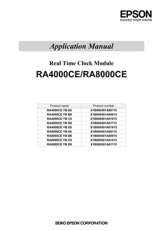
  • 1. Real Time Clock Module RA4000CE/RA8000CE Product name Product number RA4000CE YB A0 X1B000491A00115 RA4000CE YB B8 X1B000491A00915 RA4000CE YB C0 X1B000491A01015 RA4000CE YB D0 X1B000491A01115 RA4000CE YB E8 X1B000491A01915 RA8000CE YB A0 X1B000501A00115 RA8000CE YB B8 X1B000501A00915 RA8000CE YB C0 X1B000501A01015 RA8000CE YB D0 X1B000501A01115 Application Manual
  • 2. NOTICE:PLEASE READ CAREFULLY BELOW BEFORE THE USE OF THIS DOCUMENT 1. The content of this document is subject to change without notice. Before purchasing or using Epson products, please contact with sales representative of Seiko Epson Corporation (“Epson”) for the latest information and be always sure to check the latest information published on Epson’s official web sites and resources. 2. This document may not be copied, reproduced, or used for any other purposes, in whole or in part, without Epson’s prior consent. 3. Information provided in this document including, but not limited to application circuits, programs and usage, is for reference purpose only. Epson makes no guarantees against any infringements or damages to any third parties’ intellectual property rights or any other rights resulting from the information. This document does not grant you any licenses, any intellectual property rights or any other rights with respect to Epson products owned by Epson or any third parties. 4. Using Epson products, you shall be responsible for safe design in your products; that is, your hardware, software, and/or systems shall be designed enough to prevent any critical harm or damages to life, health or property, even if any malfunction or failure might be caused by Epson products. In designing your products with Epson products, please be sure to check and comply with the latest information regarding Epson products (including, but not limited to this document, specifications, data sheets, manuals, and Epson’s web site). Using technical contents such as product data, graphic and chart, and technical information, including programs, algorithms and application circuit examples under this document, you shall evaluate your products thoroughly both in stand-alone basis and within your overall systems. You shall be solely responsible for deciding whether to adopt/use Epson products with your products. 5. Epson has prepared this document carefully to be accurate and dependable, but Epson does not guarantee that the information is always accurate and complete. Epson assumes no responsibility for any damages you incurred due to any misinformation in this document. 6. No dismantling, analysis, reverse engineering, modification, alteration, adaptation, reproduction, etc., of Epson products is allowed. 7. Epson products have been designed, developed and manufactured to be used in general electronic applications and specifically designated applications (“Anticipated Purpose”). Epson products are NOT intended for any use beyond the Anticipated Purpose that requires particular quality or extremely high reliability in order to refrain from causing any malfunction or failure leading to critical harm to life and health, serious property damage, or severe impact on society, including, but not limited to listed below (“Specific Purpose”). Therefore, you are strongly advised to use Epson products only for the Anticipated Purpose. Should you desire to purchase and use Epson products for Specific Purpose, Epson makes no warranty and disclaims with respect to Epson products, whether express or implied, including without limitation any implied warranty of merchantability or fitness for any Specific Purpose. Please be sure to contact our sales representative in advance, if you desire Epson products for Specific Purpose: Space equipment (artificial satellites, rockets, etc.) / Transportation vehicles and their control equipment / Medical equipment / Relay equipment to be placed on sea floor / Power station control equipment / Disaster or crime prevention equipment / Traffic control equipment / Financial equipment Other applications requiring similar levels of reliability as the above 8. Epson products listed in this document and our associated technologies shall not be used in any equipment or systems that laws and regulations in Japan or any other countries prohibit to manufacture, use or sell. Furthermore, Epson products and our associated technologies shall not be used for the purposes of military weapons development (e.g. mass destruction weapons), military use, or any other military applications. If exporting Epson products or our associated technologies, please be sure to comply with the Foreign Exchange and Foreign Trade Control Act in Japan, Export Administration Regulations in the U.S.A (EAR) and other export-related laws and regulations in Japan and any other countries and to follow their required procedures. 9. Epson assumes no responsibility for any damages (whether direct or indirect) caused by or in relation with your non-compliance with the terms and conditions in this document or for any damages (whether direct or indirect) incurred by any third party that you give, transfer or assign Epson products. 10. For more details or other concerns about this document, please contact our sales representative. 11. Company names and product names listed in this document are trademarks or registered trademarks of their respective companies. ©Seiko Epson Corporation 2021, All rights reserved.
  • 3. RA4000CE/RA8000CE Jump to Top / Bottom ETM64E-01 Seiko Epson Corporation i ETM64E Revision History Rev. No. Date Page Description 01 Dec. 06, 2021 All New established
  • 4. RA4000CE/RA8000CE Jump to Top / Bottom ETM64E-01 Seiko Epson Corporation ii Preface This document is the application manual for describing the functions, control method, specifications, and electrical characteristics of Seiko Epson Real-Time Clock (RTC) modules RA4000CE and RA8000CE. This manual is provided for designers who develop products using the RA4000CE/RA8000CE. The RA4000CE is accessed through SPI from the host; the RA8000CE is accessed through I2 C-Bus. For the operations and control methods of these interfaces, refer to a host device manual or other documents. Notational conventions and symbols in this manual Notation of Numbers This manual describes numbers in decimal, binary, and hexadecimal notations. Decimal Examples: 1, 10, 123 (general values, date and time, etc.) Binary Examples: 0b0, 0b10, 0b1111 (control bit setting values, read values, etc.) Hexadecimal Examples: 0x0, 0xF, 0xFF (addresses, register setting values, etc.) Notation of Register and Bit Names This manual describes register and bit names as shown below. Register name: Register SEC Bit name: TSTP_INTE.STOP bit This represents the STOP bit in Register TSTP_INTE. TCTL.FSEL[1:0] bits This represents two bits in Register TCTL: FSEL1 and FSEL0 bits. Notation of Channel Numbers The time stamp function has provided a pin and control bit for each channel that has the same function as the other channels. The pin and bit names contain a channel number (e.g., 1 and 2). This manual uses “n” for the channel numbers to explain the pins and bits for all channels collectively, if there is no need to be individually described. Furthermore, “***” is used as a different part of a bit name for describing plural bit names that have a same part. Pin name: EVIN1 and EVIN2 → EVINn Bit name: EVINn_EN.EVIN1EN and EVINn_EN.EVIN2EN → EVINn_EN.EVINnEN EVINn_EN.EVIN1CPEN, CAP_EN.VTMPLCPEN, and others → ***CPEN
  • 5. RA4000CE/RA8000CE Jump to Top / Bottom ETM64E-01 Seiko Epson Corporation iii Table of Contents ETM64E Revision History ....................................................................................................................i Preface ................................................................................................................................................ii Notational conventions and symbols in this manual...........................................................................ii Notation of Numbers ....................................................................................................................ii Notation of Register and Bit Names.............................................................................................ii Notation of Channel Numbers......................................................................................................ii Table of Contents ...............................................................................................................................iii 1 Overview .......................................................................................................................1 1.1 Features ....................................................................................................................................... 1 1.2 Block Diagram............................................................................................................................. 2 RA4000CE (3-wire SPI) .............................................................................................................. 2 RA4000CE (4-wire SPI) .............................................................................................................. 3 RA8000CE (I2C-Bus) .................................................................................................................. 4 1.3 Pin................................................................................................................................................. 5 1.3.1 Pin Alignment Diagram........................................................................................................... 5 RA4000CE .................................................................................................................................. 5 RA8000CE .................................................................................................................................. 5 1.3.2 Pin Descriptions...................................................................................................................... 6 Symbol Meanings........................................................................................................................ 6 2 Power Supply and Initialization...................................................................................8 2.1 Power Supply .............................................................................................................................. 8 2.2 Initialization ................................................................................................................................. 8 2.2.1 Power-On Sequence .............................................................................................................. 8 2.2.2 Oscillation Start-UP Time ....................................................................................................... 9 2.2.3 Initial Settings ........................................................................................................................11 Initial Setting Procedure (for models without the /RST output function) ................................... 11 Initial Setting Procedure (for models with the /RST output function) ........................................ 12 2.3 Operating Mode......................................................................................................................... 13 POR enabled............................................................................................................................. 14 Initial mode................................................................................................................................ 14 Normal mode............................................................................................................................. 14 Safe mode................................................................................................................................. 14 3 Functions ....................................................................................................................15 3.1 Host Interface ............................................................................................................................ 15 3.1.1 Accessing to RA4000CE Registers (SPI) ............................................................................ 15 SPI Interface Pins ..................................................................................................................... 15 Writing Data to Registers .......................................................................................................... 16 Reading Data from Registers.................................................................................................... 17 3.1.2 Accessing to RA8000CE Registers (I2 C-Bus)...................................................................... 18 I2C-Bus Interface Pins............................................................................................................... 18 Slave Address ........................................................................................................................... 18 Writing Data to Registers .......................................................................................................... 18 Reading Data from Registers.................................................................................................... 19 3.2 Clock and Calendar Function.................................................................................................. 20 3.2.1 Overview............................................................................................................................... 20 3.2.2 Operations ............................................................................................................................ 22 BCD Mode and BIN Mode ........................................................................................................ 22 Accessing Clock/Calendar Counter through Clocking Buffer ................................................... 22 Initial Setting and Starting Clock/Calendar ............................................................................... 24 Reading Clock/Calendar Data .................................................................................................. 26 Reading/Writing 1/1024-Second Data ...................................................................................... 27 1/1024-Second Offset Time Adjustment ................................................................................... 28 Clock/Calendar Counter Stop Procedure.................................................................................. 29 Leap Year Determination .......................................................................................................... 29
  • 6. RA4000CE/RA8000CE Jump to Top / Bottom ETM64E-01 Seiko Epson Corporation iv Leap Second Correction Procedure.......................................................................................... 29 3.3 Temperature Compensation Function.................................................................................... 30 3.3.1 Operations ............................................................................................................................ 30 Setting Temperature Compensation Interval............................................................................. 30 Temperature Compensation Operation Flag: VTMPLF flag (0x0E).......................................... 30 3.4 Theoretical Regulation Function............................................................................................. 31 3.4.1 Operations ............................................................................................................................ 31 Theoretical Regulation Operation ............................................................................................. 31 Setting Correction Amount ........................................................................................................ 31 Enabling Theoretical Regulation ............................................................................................... 32 Disabling Theoretical Regulation .............................................................................................. 32 3.4.2 Influence of Theoretical Regulation to Other Functions....................................................... 32 3.5 Time Update Interrupt Function .............................................................................................. 33 3.5.1 Overview............................................................................................................................... 33 3.5.2 Operations ............................................................................................................................ 33 Selecting Interrupt Period ......................................................................................................... 33 Interrupt Enabling/Disabling Procedure .................................................................................... 33 Interrupt Operations .................................................................................................................. 34 3.6 Alarm Function.......................................................................................................................... 35 3.6.1 Overview............................................................................................................................... 35 3.6.2 Operations ............................................................................................................................ 35 Alarm Setting Procedure........................................................................................................... 35 Alarm Setting Examples............................................................................................................ 36 Alarm Interrupt .......................................................................................................................... 37 3.7 Wakeup Timer Function ........................................................................................................... 38 3.7.1 Overview............................................................................................................................... 38 3.7.2 Operations ............................................................................................................................ 38 Source Clock............................................................................................................................. 38 Count-Up/Down Mode .............................................................................................................. 39 Preset Data (wakeup timer interrupt period)............................................................................. 39 Counting Condition (only for the models with the /RST output function) .................................. 39 Wakeup Timer Setting Procedure ............................................................................................. 40 Starting Count ........................................................................................................................... 40 Suspension ............................................................................................................................... 41 Reading Counter Data .............................................................................................................. 42 Resetting Counter ..................................................................................................................... 42 Wakeup Timer Interrupt............................................................................................................. 43 3.8 FOUT Output Function ............................................................................................................. 45 3.8.1 Overview............................................................................................................................... 45 3.8.2 Operations ............................................................................................................................ 45 Initial Settings............................................................................................................................ 45 Controlling FOUT Output (when not using the FOE pin) .......................................................... 45 Controlling FOUT Output (when using the FOE pin) ................................................................ 46 Wakeup Timer Interrupt Signal Output from FOUT pin............................................................. 46 3.9 Reset Output Function ............................................................................................................. 47 3.9.1 Overview............................................................................................................................... 47 3.9.2 Operations ............................................................................................................................ 47 VDD Voltage Detection Operation for Reset Output................................................................... 47 Reset Output Flag..................................................................................................................... 47 I/O Control During Reset Output............................................................................................... 47 3.10 Self-Monitoring Function ......................................................................................................... 48 3.10.1 Overview............................................................................................................................... 48 3.10.2 Self-Monitoring Flags............................................................................................................ 48 Power-On Reset Detection: PORF flag .................................................................................... 48 Crystal Oscillation Stop Detection: OSCSTPF flag................................................................... 48 Invalid Date and Time Data Warning: VLF Flag........................................................................ 48 Temperature Compensation Update Stop Detection: VTMPLF flag ......................................... 48 3.10.3 Self-Monitoring Flag Output Function .................................................................................. 48
  • 7. RA4000CE/RA8000CE Jump to Top / Bottom ETM64E-01 Seiko Epson Corporation v 3.11 Time Stamp Function ............................................................................................................... 49 3.11.1 Overview............................................................................................................................... 49 3.11.2 Time Stamp Triggers ............................................................................................................ 50 External Event Inputs (EVINn pin) Trigger................................................................................ 50 Internal Event Trigger................................................................................................................ 51 Command trigger ...................................................................................................................... 51 3.11.3 Time Stamp Buffer................................................................................................................ 52 Time Stamp Data ...................................................................................................................... 52 Time Stamp Buffer Operating Mode ......................................................................................... 53 Time Stamp Buffer Write Mode................................................................................................. 53 3.11.4 Operations ............................................................................................................................ 54 Initial Settings............................................................................................................................ 54 Time Stamp Capturing Operation ............................................................................................. 56 Issuing Command Trigger......................................................................................................... 59 Reading Time Stamp Data........................................................................................................ 60 3.11.5 Time Stamp (Event Detection) Interrupts............................................................................. 62 3.11.6 Reading/Writing in SRAM Mode........................................................................................... 63 3.12 SOUT Output Function............................................................................................................. 64 Status Output ............................................................................................................................ 64 DC Output ................................................................................................................................. 64 4 Registers.....................................................................................................................65 4.1 List of Registers........................................................................................................................ 65 Symbol meanings...................................................................................................................... 65 Bank 0 ....................................................................................................................................... 65 Bank 1 ....................................................................................................................................... 66 Bank 2 ....................................................................................................................................... 66 Bank 3 ....................................................................................................................................... 67 Bank 4 ....................................................................................................................................... 67 Bank 5 ....................................................................................................................................... 67 Bank 6/7 (when reading time stamp (BCD) data in Direct mode)............................................. 68 Bank 6/7 (when reading time stamp data (BIN) in Direct mode) .............................................. 68 Bank 6 (SRAM mode) ............................................................................................................... 69 4.2 Description of Registers .......................................................................................................... 70 0x00: SEC (Second Data) [BCD mode] ................................................................................. 70 0x01: MIN (Minute Data) [BCD mode].................................................................................... 70 0x02: HOUR (Hour Data) [BCD mode]................................................................................... 70 0x03: WEEKDAY (Day-of-Week Data) [BCD mode] .............................................................. 70 0x04: DAY (Day Data) [BCD mode] ....................................................................................... 71 0x05: MONTH (Month Data) [BCD mode].............................................................................. 71 0x06: YEAR (Year Data) [BCD mode].................................................................................... 71 0x00: SEC_BIN0 (Second Binary Data 0) [BIN mode]........................................................... 72 0x01: SEC_BIN1 (Second Binary Data 1) [BIN mode]........................................................... 72 0x02: SEC_BIN2 (Second Binary Data 2) [BIN mode]........................................................... 72 0x03: SEC_BIN3 (Second Binary Data 3) [BIN mode]........................................................... 72 0x04: SEC_BIN4 (Second Binary Data 4) [BIN mode]........................................................... 72 0x07: ALM_MIN (Minute Alarm) [BCD mode]......................................................................... 72 0x08: ALM_HOUR (Hour Alarm) [BCD mode]........................................................................ 73 0x09: ALM_WEEKDAY (Day-of-Week Alarm / Day Alarm) [BCD mode]................................ 73 0x0A: WTCNT_L (Wakeup Timer Counter Low)....................................................................... 74 0x0B: WTCNT_M (Wakeup Timer Counter Middle).................................................................. 74 0x0C: WTCNT_H (Wakeup Timer Counter High) ..................................................................... 74 0x0D: TCTL (Timer Control)...................................................................................................... 75 0x0E: INTF (Status Flag) .......................................................................................................... 76 0x0F: TSTP_INTE (Timer Stop and Interrupt Enable) .............................................................. 77 0x10: SUBSEC_L (Sub-Second Data Low) .............................................................................. 78 0x11: SUBSEC_H (Sub-Second Data High)............................................................................. 78 0x12: SEC_MIR (Mirrored Second Data, = 0x00) [BCD mode] ............................................. 78 0x13: MIN_MIR (Mirrored Minute Data, = 0x0h) [BCD mode] ............................................... 78 0x14: HOUR_MIR (Mirrored Hour Data, = 0x02) [BCD mode] .............................................. 79 0x15: WEEKDAY_MIR (Mirrored Day-of-Week Data, = 0x03) [BCD mode].......................... 79
  • 8. RA4000CE/RA8000CE Jump to Top / Bottom ETM64E-01 Seiko Epson Corporation vi 0x16: DAY_MIR (Mirrored Day Data, = 0x04) [BCD mode] ................................................... 79 0x17: MONTH_MIR (Mirrored Month Data, = 0x05) [BCD mode].......................................... 79 0x18: YEAR_MIR (Mirrored Year Data, = 0x06) [BCD mode]................................................ 79 0x12: SEC_BIN0_MIR (Mirrored Second Binary Data 0, = 0x00) [BIN mode] ...................... 79 0x13: SEC_BIN1_MIR (Mirrored Second Binary Data 1, = 0x01) [BIN mode] ...................... 79 0x14: SEC_BIN2_MIR (Mirrored Second Binary Data 2, = 0x02) [BIN mode] ...................... 79 0x15: SEC_BIN3_MIR (Mirrored Second Binary Data 3, = 0x03) [BIN mode] ...................... 79 0x16: SEC_BIN4_MIR (Mirrored Second Binary Data 4, = 0x04) [BIN mode] ...................... 79 0x19: OFS_SUBSEC_H (Offset Sub-Second Data High) ........................................................ 80 0x1A: OFS_SUBSEC_L (Offset Sub-Second Data Low).......................................................... 80 0x1B: DIG_TRIM_H (Digital Trimming Data High).................................................................... 81 0x1C: DIG_TRIM_L (Digital Trimming Data Low) ..................................................................... 81 0x1D: TCTL_MIR (Mirrored Timer Control, = 0x0D) ................................................................. 81 0x1E: INTF_MIR (Mirrored Status Flag, = 0x0E)...................................................................... 81 0x1F: CNTSEL (Counter Select)............................................................................................... 81 0x20: EVIN_EN (Event Input Enable)....................................................................................... 82 0x21: EVIN1_CFG (EVIN1 Configuration)................................................................................ 82 0x23: EVIN2_CFG (EVIN2 Configuration)................................................................................ 82 0x22: EVIN1_FLT (EVIN1 Noise Filter)..................................................................................... 83 0x24: EVIN2_FLT (EVIN2 Noise Filter)..................................................................................... 83 0x27: BUF1_CFG1 (BUF1 Configuration 1) ............................................................................. 83 0x28: BUF1_STAT (BUF1 Status)............................................................................................. 84 0x29: BUF1_CFG2 (BUF1 Configuration 2) ............................................................................. 85 0x30: ALM_SEC (Second Alarm).............................................................................................. 85 0x31: ALM_MIN_MIR (Mirrored Minute Alarm, = 0x07)............................................................ 85 0x32: ALM_HOUR_MIR (Mirrored Hour Alarm, = 0x08)........................................................... 85 0x33: ALM_WEEKDAY_MIR (Mirrored Day-of-Week Alarm / Day Alarm, = 0x09)................... 86 0x34: UPDISEL (Time Update Interrupt Select) ....................................................................... 86 0x38: WTICFG (Wakeup Timer Interrupt Configuration) .......................................................... 86 0x39: WTCTL (Wakeup Timer Control)..................................................................................... 87 0x3A: WTCNT_L_MIR (Mirrored Wakeup Timer Counter Low, = 0x0A) .................................. 88 0x3B: WTCNT_M_MIR (Mirrored Wakeup Timer Counter Middle, = 0x0B) ............................. 88 0x3C: WTCNT_H_MIR (Mirrored Wakeup Timer Counter High, = 0x0C) ................................ 88 0x3D: TCTL_MIR (Mirrored Timer Control, = 0x0D) ................................................................. 89 0x3E: INTF_MIR (Mirrored Status Flag, = 0x0E)...................................................................... 89 0x3F: TSTP_INTE_MIR (Mirrored Timer Stop and Interrupt Enable, = 0x0F).......................... 89 0x41: WRCMD_CFG (Write Command Configuration) ............................................................ 89 0x42: WRCMD_TRG (Write Command Trigger)....................................................................... 90 0x43: EVNT_INTE (Event Interrupt Enable) ............................................................................. 90 0x44: CAP_EN (Capture Enable) ............................................................................................. 91 0x45: INTF_MIR (Mirrored Status Flag, = 0x0E) ...................................................................... 91 0x46: BUF_INTF (Buffer Interrupt Factor) ................................................................................ 91 0x47: EVNT_INTF (Event Interrupt Factor) .............................................................................. 92 0x51: EVIN1_EVCNT (EVIN1 Event Counter).......................................................................... 93 0x52: EVIN2_EVCNT (EVIN2 Event Counter).......................................................................... 93 0x54: EVINMON (EVIN Monitor)............................................................................................... 93 0x55: SOUTCTL (SOUT Control).............................................................................................. 93 5 Electrical Characteristics...........................................................................................95 5.1 Absolute Maximum Ratings..................................................................................................... 95 5.2 Recommended Operating Conditions.................................................................................... 95 5.3 Frequency Characteristics....................................................................................................... 95 5.4 DC Characteristics.................................................................................................................... 96 DC Characteristics .................................................................................................................... 96 Temperature Compensation Operation and Current Consumption .......................................... 97 Current Consumption of Model with /RST Output Pin .............................................................. 97 Detection Voltages for State Transition and Self-Monitoring Functions.................................... 97 5.5 AC Characteristics.................................................................................................................... 98 RA4000CE AC Characteristics ................................................................................................. 98 RA8000CE AC Characteristics ................................................................................................. 99
  • 9. RA4000CE/RA8000CE Jump to Top / Bottom ETM64E-01 Seiko Epson Corporation vii 5.6 Power-On Characteristics...................................................................................................... 100 5.7 Reset Output Characteristics ................................................................................................ 101 6 Package.....................................................................................................................102 6.1 Package Dimensions.............................................................................................................. 102 6.2 Marking Layout ....................................................................................................................... 102 7 Notes on Mounting...................................................................................................103 Static Electricity....................................................................................................................... 103 Noise ....................................................................................................................................... 103 Input Voltage ........................................................................................................................... 103 Handling of Unused Pins ........................................................................................................ 103 Soldering Temperature............................................................................................................ 103 Mounting Equipment ............................................................................................................... 103 Ultrasonic Cleaning................................................................................................................. 103 Mounting Orientation............................................................................................................... 103 Leakage between Pins............................................................................................................ 103 Solder Heat Resistance Evaluation Profile (for reference) ..................................................... 104 8 Moisture Resistance/Electrostatic Breakdown Voltage Characteristics .............105 8.1 Moisture Sensitivity Level (MSL)........................................................................................... 105 8.2 Electrostatic Breakdown Voltage.......................................................................................... 105 9 Sample Connection Diagram...................................................................................106 10 Packing Information (reference) .............................................................................108 Taping Specification (TE0804L) .............................................................................................. 108 Reel Specification ................................................................................................................... 108 List of Figures/Tables ...................................................................................................109 Figures .................................................................................................................................... 109 Tables...................................................................................................................................... 110
  • 10. 1 Overview RA4000CE/RA8000CE Jump to Top / Bottom ETM64E-01 Seiko Epson Corporation 1 1 Overview The RA4000CE/RA8000CE is a real-time clock module with integrated 32.768 kHz digital temperature compensated crystal oscillator (DTCXO) and conforms to the AEC-Q100 standard. It includes various functions such as a second-to- year clock/calendar with a leap-year correction, time alarm, wakeup timer, time update interrupts, clock output, and a time stamp function that can record two times and dates when an external or internal event occurs, and the power supply statuses that have been detected by the self-monitoring function. This product is capable of low power operation and conforms to the AEC-Q100 standard, thus it is usable for on-vehicle applications as well as various time keeping applications. RA4000CE YB A 0 ① ② ③④ ① Model CE type package 3.2 x 2.5 x 1.0 mm ② Frequency tolerance ③ Pin Option A: Option A-E ④ Reset output function 0: No /RST pin 8: With /RST pin (VDD drop detection voltage: +2.4 V Typ.) Table 1.1 Product Lineup Product name Interface Frequency accuracy *1 External event input (EVINn) Reset output (/RST) Clock output (FOUT or /INT) FOUT enable (FOE) Status output (SOUT) RA4000CE Option A YB 3-wire SPI YB 2 inputs – ✓ – – RA4000CE Option B YB YB 2 inputs ✓ ✓ – – RA4000CE Option C YB YB – – ✓ – – RA4000CE Option D YB 4-wire SPI YB 1 input – ✓ – ✓ RA4000CE Option E YB YB 1 input ✓ ✓ – ✓ RA8000CE Option A YB I2 C-Bus*2 YB 2 inputs – ✓ – ✓ RA8000CE Option B YB YB 2 inputs ✓ ✓ – ✓ RA8000CE Option C YB YB – – ✓ – – RA8000CE Option D YB YB 1 input – ✓ ✓ ✓ ✓: Available, –: Unavailable *1 For the accuracy (YB), refer to the frequency tolerance shown in “5.3 Frequency Characteristics.” *2 I2 C-Bus is a trademark of NXP Semiconductors. 1.1 Features Table 1.2 Features Product lineup RA4000CE RA8000CE Host interface 3-wire SPI or 4-wire SPI *1 I2 C-Bus *1 Crystal oscillator • A 32.768 kHz digital temperature compensated crystal oscillator (DTCXO) is included. Clock/calendar • BCD counters for counting seconds, minutes, hours, days, months, and years, and a day-of-week counter are included. [BCD mode] • A binary counter for counting 1/1024 seconds is included. • A binary counter for counting seconds such as UNIX time is included. [BIN mode] • An automatic leap year correction function is included and a leap second correction method is provided. [BCD mode] • Time update interrupts can be generated. (1-second, 1-minute, or 1-hour counter update intervals) [BCD mode] • A theoretical regulation function is included. Wakeup timer • Can generate an interrupt in 976.56 µs to 32-year cycle. • Can be used as a time integration meter. • Can be used as a watchdog timer. • Can be used as a universal counter for counting EVIN2 pin inputs (external event inputs). Alarm Can generate an interrupt at the specified day (or day of the week), hour, minute, and second. [BCD mode] Time stamp Trigger source • External event (EVINn) input *1 • Voltage drop detection/oscillation stop detection • Command input from the host Record data • 1/1024-second data
  • 11. 1 Overview RA4000CE/RA8000CE Jump to Top / Bottom ETM64E-01 Seiko Epson Corporation 2 Product lineup RA4000CE RA8000CE • Time data (seconds, minutes, hours, days, months, and years [BCD mode] or binary time [BIN mode]) • Trigger source • Internal status Number of recordable events Two events Clock output (FOUT) *1 • Selectable from 32.768 kHz, 1024 Hz, and 1 Hz outputs • Output can be controlled by a register. Status output (SOUT) *1 Can output the selected internal flag (interrupt flag, voltage drop detection flag) status. Reset output *1 Can output a reset signal when a VDD voltage drop status is detected. Self-monitoring function Can generate an interrupt when the oscillation stops or a VDD voltage drop status is detected. Operating voltage (VDD) 1.60 V to 5.5 V Operating temperature -40 °C to +125 °C *1 See Table 1.1. 1.2 Block Diagram RA4000CE (3-wire SPI) Figure 1.1 RA4000CE Option A/B/C Block Diagram 32.768 kHz RA4000CE Option A/B/C /INT FOUT /RST Interrupt controller Event trigger controller Pull-up/down control FOUT controller Oscillator (DTCXO) Divider Theoretical regulation Clock/ calendar Wakeup timer Alarm Time stamp GND GND GND VDD Option A/B Power controller/ voltage detector EVIN1 EVIN2 Option B /RST controller VDD GND Bus interface (3-wire SPI) CE CLK DIO GND
  • 12. 1 Overview RA4000CE/RA8000CE Jump to Top / Bottom ETM64E-01 Seiko Epson Corporation 3 RA4000CE (4-wire SPI) Figure 1.2 RA4000CE Option D/E Block Diagram 32.768 kHz RA4000CE Option D/E /INT /RST SOUT Interrupt controller Event trigger controller Pull-up/down control Oscillator (DTCXO) Divider Theoretical regulation Clock/ calendar Wakeup timer Alarm Time stamp GND GND GND VDD Power controller/ voltage detector EVIN2 SOUT controller /RST controller VDD GND Bus interface (4-wire SPI) GND CE CLK DO DI Option E
  • 13. 1 Overview RA4000CE/RA8000CE Jump to Top / Bottom ETM64E-01 Seiko Epson Corporation 4 RA8000CE (I2C-Bus) Figure 1.3 RA8000CE Option A/B/C/D Block Diagram 32.768 kHz RA8000CE Option A/B/C/D /INT FOUT /RST SOUT Interrupt controller Event trigger controller Bus interface (I2C) Pull-up/down control FOUT controller Oscillator (DTCXO) Divider Theoretical regulation Clock/ calendar Wakeup timer Alarm Time stamp GND GND GND GND VDD SCL SDA Power controller/ voltage detector EVIN2 SOUT controller /RST controller VDD GND Option A/B/D Option A/B EVIN1 Option D Option B Option A/B/D FOE
  • 14. 1 Overview RA4000CE/RA8000CE Jump to Top / Bottom ETM64E-01 Seiko Epson Corporation 5 1.3 Pin 1.3.1 Pin Alignment Diagram RA4000CE Pin name No. No. Pin name EVIN1 1 10 /INT VDD 2 9 GND CE 3 8 CLK FOUT 4 7 DIO N.C. 5 6 EVIN2 Option A Pin name No. No. Pin name EVIN1 1 10 /INT VDD 2 9 GND CE 3 8 CLK FOUT 4 7 DIO /RST 5 6 EVIN2 Option B Pin name No. No. Pin name N.C. 1 10 N.C. VDD 2 9 GND CE 3 8 CLK /INT 4 7 DIO N.C. 5 6 N.C. Option C Pin name No. No. Pin name DI 1 10 SOUT VDD 2 9 GND CE 3 8 CLK /INT 4 7 DO N.C. 5 6 EVIN2 Option D Pin name No. No. Pin name DI 1 10 SOUT VDD 2 9 GND CE 3 8 CLK /INT 4 7 DO /RST 5 6 EVIN2 Option E Figure 1.4 RA4000CE Pin Alignment Diagrams RA8000CE Pin name No. No. Pin name EVIN1 1 10 SOUT VDD 2 9 GND /INT 3 8 SCL FOUT 4 7 SDA N.C. 5 6 EVIN2 Option A Pin name No. No. Pin name EVIN1 1 10 SOUT VDD 2 9 GND /INT 3 8 SCL FOUT 4 7 SDA /RST 5 6 EVIN2 Option B Pin name No. No. Pin name N.C. 1 10 N.C. VDD 2 9 GND /INT 3 8 SCL FOUT 4 7 SDA N.C. 5 6 N.C. Option C Pin name No. No. Pin name FOE 1 10 SOUT VDD 2 9 GND /INT 3 8 SCL FOUT 4 7 SDA N.C. 5 6 EVIN2 Option D Figure 1.5 RA8000CE Pin Alignment Diagrams * The N.C. pins (Pins 1, 5, and 6) of the models in Option A, C, or D are always pulled down with a built-in pull-down resister. Therefore, these pins should be left open (do not electrically connect anything).
  • 15. 1 Overview RA4000CE/RA8000CE Jump to Top / Bottom ETM64E-01 Seiko Epson Corporation 6 1.3.2 Pin Descriptions Symbol Meanings I/O I: Input pin O: Output pin I/O: Input/output pin Initial state Hi-Z: High impedance PU: Pulled up PD: Pulled down Model-specific column ✓: Available –: Unavailable Table 1.3 Pin Descriptions Pin name I/O Initial state Function RA4000CE RA8000CE A B C D E A B C D EVIN1 I PU (1 MΩ) External event input pins These pins are used to input time stamp trigger signals (detectable even in reset output state (Safe mode)). Programmable pull-up and pull-down resistors and noise filters are included. ✓ ✓ – – – ✓ ✓ – – EVIN2 ✓ ✓ – ✓ ✓ ✓ ✓ – ✓ CLK I Hi-Z 3-wire/4-wire SPI serial clock input pin In Normal mode, placing this pin into a floating state is not allowed. In Safe mode with the WTICFG.RSTOPT1 bit set to 0, this pin is disabled to input, thus a floating state is allowed. ✓ ✓ ✓ ✓ ✓ – – – – DIO I/O Hi-Z 3-wire SPI serial data input/output pin In Normal mode and when this pin is in input state, placing this pin into a floating state is not allowed. In Safe mode with the WTICFG.RSTOPT1 bit set to 0, this pin is disabled to input, thus a floating state is allowed. ✓ ✓ ✓ – – – – – – DO O Hi-Z 4-wire SPI serial data output pin In Safe mode with the WTICFG.RSTOPT1 bit set to 0, this pin is disabled to output and set into a Hi-Z state. – – – ✓ ✓ – – – – DI I Hi-Z 4-wire SPI serial data input pin In Normal mode, placing this pin into a floating state is not allowed. In Safe mode with the WTICFG.RSTOPT1 bit set to 0, this pin is disabled to input, thus a floating state is allowed. – – – ✓ ✓ – – – – CE I PD (300 kΩ) 3-wire/4-wire SPI slave select input pin A pull-down resistor is included. In Safe mode with the WTICFG.RSTOPT1 bit set to 0, this pin is disabled to input, thus a floating state is allowed. ✓ ✓ ✓ ✓ ✓ – – – – SCL I Hi-Z I2 C-Bus serial clock input pin In Normal mode, placing this pin into a floating state is not allowed. In Safe mode with the WTICFG.RSTOPT1 bit set to 0, this pin is disabled to input, thus a floating state is allowed. This pin can be externally pulled up to a voltage up to 5.5 V. – – – – – ✓ ✓ ✓ ✓ SDA I/O Hi-Z I2 C-Bus serial data input/output pin (N-ch. open drain) This pin inputs or outputs addresses, data, acknowledgement and other bits in sync with the SCL signal. This pin is an N-ch open drain output and can be externally pulled up to a voltage up to 5.5 V. In Safe mode with the WTICFG.RSTOPT1 bit set to 0, this pin is disabled to input, thus a floating state is allowed. – – – – – ✓ ✓ ✓ ✓ FOUT O Hi-Z Clock output pin (CMOS) 32.768 kHz, 1024 Hz or 1 Hz clock output is selectable. Can be switched to the wakeup timer interrupt output (CMOS). In Safe mode with the WTICFG.RSTOPT0 bit set to 0, this pin is disabled to output and set into a Hi-Z state. ✓ ✓ – – – ✓ ✓ ✓ ✓ FOE I Hi-Z FOUT output enable input pin When an H level is input, the FOUT pin outputs a square wave with the frequency set by a register. When an L level is input, the FOUT pin is set into a Hi-Z state. In Safe mode with the WTICFG.RSTOPT1 bit set to 0, this pin is disabled to input, thus a floating state is allowed. – – – – – – – – ✓
  • 16. 1 Overview RA4000CE/RA8000CE Jump to Top / Bottom ETM64E-01 Seiko Epson Corporation 7 Pin name I/O Initial state Function RA4000CE RA8000CE A B C D E A B C D /INT O Hi-Z Interrupt output pin (N-ch. open drain) The wakeup timer, time update, alarm, and/or event detection interrupt signals can be selected to output from this pin. When two or more signals are selected, they are NORed before being output. In Safe mode with the WTICFG.RSTOPT0 bit set to 0, this pin is disabled to output and set into a Hi-Z state. This pin can be externally pulled up to a voltage up to 5.5 V. ✓ ✓ ✓ ✓ ✓ ✓ ✓ ✓ ✓ SOUT O Hi-Z Status output pin One of the internal flags (TF/AF/UF/EF/VTMPLF/VLF) can be selected to output its status from this pin. The output signal polarity can also be selected. In Safe mode with the WTICFG.RSTOPT0 bit set to 0, this pin is disabled to output and set into a Hi-Z state. – – – ✓ ✓ ✓ ✓ – ✓ /RST (I) /O Hi-Z Reset output pin (N-ch open drain) A reset signal can be output to external devices when a VDD voltage drop below the predefined value is detected. When the VDD voltage is restored (a VDD voltage rise to the predefined value is detected), the reset output is cancelled (set to a Hi-Z state) after 60 ms from the detection. This pin is an N-ch open drain output. Connect an appropriate pull-up resistor according to the capacity of the signal line. The external pull-up voltage should be the VDD level of the RTC or higher. When the reset output function is not used in the model with the /RST pin (RA4000CE-B, E, RA8000CE-B), this pin should be fixed at a GND level. – ✓ – – ✓ – ✓ – – VDD – – Main power supply pin ✓ ✓ ✓ ✓ ✓ ✓ ✓ ✓ ✓ GND – – Ground pin ✓ ✓ ✓ ✓ ✓ ✓ ✓ ✓ ✓ Notes: • Do not leave the unused input and input/output pins open nor apply an intermediate potential to them if the internal pull-up or -down resistor is not enabled. • Leave the output pins (FOUT, SOUT, /INT, and DO) open when they are not used. • When the reset output function is not used in the model with the /RST pin function, the /RST pin should be fixed at a GND level. • The input pins allow applying a voltage up to 5.5 V regardless of the VDD voltage level. • The /INT output pin can be pulled up to a voltage up to 5.5 V regardless of the VDD voltage level. • The /RST output pin can be pulled up to a voltage within the range from VDD to 5.5 V. • Pin 5 of the models without the /RST pin function should be left open, as it outputs an L level.
  • 17. 2 Power Supply and Initialization RA4000CE/RA8000CE Jump to Top / Bottom ETM64E-01 Seiko Epson Corporation 8 2 Power Supply and Initialization 2.1 Power Supply The table below lists the RA4000CE/RA8000CE power supply pins. Table 2.1 List of Power Supply Pins Pin name Function VDD Main power supply pin GND Ground pin The RA4000CE/RA8000CE operates with the power supply voltage applied to the VDD pin. For the operating power supply range, refer to “5.2 Recommended Operating Conditions.” Note: Design the PCB pattern so that a bypass capacitor will be placed as close to the VDD pin as possible. 2.2 Initialization 2.2.1 Power-On Sequence The RA4000CE/RA8000CE executes a power-on reset processing when the VDD voltage is supplied. To make certain that the RA4000CE/RA8000CE executes a power-on reset, satisfy the power-on specifications (tR1, refer to “5.6 Power-On Characteristics”). The tCL in Figure 2.1 shows the time for canceling power-on reset. Before turning the power supply back on after being turned off, be sure to maintain an OFF period with the VDD pin set to the GND level for at least 10 seconds after turning off. Then turn the power supply back on again with the power supply initial rise time specification satisfied. (1) In the case of a model without the /RST output function (2) In the case of a model with the /RST output function Figure 2.1 Power-On Sequence tR1 tR2 Interface Registers are accessible. Power supply VDD Internal POR No effect Asserted Cancelled Cancelled /RST +VDET1n tDELAYF tSTA tCD 188 ms (Max.) tDELAYS Safe mode period Normal mode period Normal mode period VPOR (Max.) VPOR (Min.) VACC (Min.) Internal Vreg Externally pulled up (VDD) VDD GND GND +VDET1n -VDET1n Registers are access ible. 128 ms (Max.) t_int tDELAY 60 ms (VDD ³ +VDET1n) tF
  • 18. 2 Power Supply and Initialization RA4000CE/RA8000CE Jump to Top / Bottom ETM64E-01 Seiko Epson Corporation 9 2.2.2 Oscillation Start-UP Time When the VDD voltage is applied, the crystal oscillation circuit starts oscillating. The host interface becomes usable after 40 ms from turning VDD on. However, a wait time is required until the internal crystal oscillation waveform has a sufficient amplitude before the clock/calendar counter value can be set and read. This refers to the oscillation start-up time (tSTA, refer to “5.3 Frequency Characteristics”). There are two methods to secure the wait time in the models without the /RST output function: one is the method for repeatedly trying to clear the INTF.OSCSTPF and INTF.VLF bits, another is the method for waiting by the host until tSTA has elapsed after applying VDD. The former can shorten the wait time until the clock/calendar counter value will be able to set and read. On the other hand, the latter can set the clock/calendar counter with higher time accuracy, as the crystal oscillation frequency becomes more stable although the wait time becomes longer The INTF.OSCSTPF and INTF.VLF bits are set to 1 by the oscillation stop detection function immediately after the crystal oscillation circuit starts oscillating. While the oscillation stop status is being detected, these bits cannot be cleared to 0 even if 0 is written to these bits through the host interface. When the oscillation stop status is cancelled by the grown internal oscillation waveform amplitude, the INTF.OSCSTPF and INTF.VLF bits can be cleared. Therefore, try to clear these bits at arbitrary time intervals until they are actually cleared. After that the clock/calendar counter value can be set and read. Make sure that the INTF.VLF bit has been cleared before the host configures the operational settings of the functions shown below (*). On the other hand in the models with the /RST output function, the host interface is disabled until the VDD voltage rises to +VDET1n or higher. When tSTA has elapsed as well as the condition of VDD ≥ +VDET1n has been satisfied, the /RST output is cancelled and communication can be established allowing access to all registers. * Functions that should be configured after the INTF.VLF bit is cleared: • Selecting the multi-function pin functions (WTICFG.PINMUX[1:0] bit settings) • Setting the required timer functions • Controlling the FOUT output (TCTL.FSEL[1:0] bit settings) • Setting the temperature compensation execution interval (TSTP_INTE.CSEL[1:0] bit settings)
  • 19. 2 Power Supply and Initialization RA4000CE/RA8000CE Jump to Top / Bottom ETM64E-01 Seiko Epson Corporation 10 (1) In the case of a model without the /RST output function All the registers can be accessed after tSTA has elapsed. (2) In the case of a model with the /RST output function Figure 2.2 Oscillation Start Sequence GND VDD Internal oscillation waveform (image) Powe supply (VDD) FOUT VACC (Min.) (Interface voltage) VCLK (Minimum time keeping voltage) tSTA: Oscillation start-up time (Oscillation stabilization waiting time) Flags such as the INTF.VLF bit are accessible for checking. Clock/calendar and other registers can be configured. 40 ms VLF “1” VLF can be cleared and registers are accessible for setting. VLF “0” GND VDD Internal oscillation waveform (image) Powe supply (VDD) FOUT VACC (Min.) (Interface voltage) VCLK (Minimum time keeping voltage) tSTA: Oscillation start-up time (Oscillation stabilization waiting time) Clock/calendar and other registers can be configured. /RST
  • 20. 2 Power Supply and Initialization RA4000CE/RA8000CE Jump to Top / Bottom ETM64E-01 Seiko Epson Corporation 11 2.2.3 Initial Settings It is necessary to initially set the registers after initial power on or when a supply voltage drop with the INTF.VLF bit set to 1 from 0 has occurred. This section shows an example of initial settings. Initial Setting Procedure (for models without the /RST output function) 1. Wait for at least 40 ms after the power is initially turned on. 2. Cancelling POR and detecting oscillation start-up (polling of the INTF.VLF bit) The INTF.VLF bit is set to 1 when a power-on reset is issued due to a power supply voltage drop or an oscillation stop is detected. 2.1. Read the INTF.VLF bit and go to Step 3 when the read value = 0. If the INTF.VLF bit = 1, perform Steps 2.2 to 2.4. 2.2. Write 0x00 to Register INTF to try and clear the INTF.VLF bit and to clear the interrupt flags. - PORF bit (Power-on reset detection flag) - OSCSTPF bit (Oscillation stop detection flag) - UF bit (Time update interrupt flag) - TF bit (Wakeup timer interrupt flag) - AF bit (Alarm interrupt flag) - EVF bit (Event detection interrupt flag) - VLF bit (RTC initialize interrupt flag) - VTMPLF bit (Temperature compensation update stop interrupt flag) 2.3. Take a waiting time. 2.4. Return to Step 2.1. 3. Disable interrupts/counters. (Write 0x00 to Register TSTP_INTE.) - CSEL[1:0] bits (Temperature sensor measurement operation interval) - UIE bit (Disable time update interrupt) - TIE bit (Disable wakeup timer interrupt) - AIE bit (Disable alarm interrupt) - EIE bit (Disable event detection interrupt) - STOP bit (Stop counters) 4. Set the current time. For more information, refer to “3.2 Clock and Calendar Function.” 5. Set alarm. For more information, refer to “3.6 Alarm Function.” 6. Set wakeup timer. For more information, refer to “3.7 Wakeup Timer Function.”
  • 21. 2 Power Supply and Initialization RA4000CE/RA8000CE Jump to Top / Bottom ETM64E-01 Seiko Epson Corporation 12 Initial Setting Procedure (for models with the /RST output function) 1. Wait for at least tSTA after the power is initially turned on. Or confirm that the /RST output is cancelled. 2. Cancelling POR and detecting oscillation start-up (polling of the INTF.VLF bit) The INTF.VLF bit is set to 1 when a power-on reset is issued due to a power supply voltage drop or an oscillation stop is detected. 2.1. Read the INTF.VLF bit and go to Step 3 when the read value = 0. If the INTF.VLF bit = 1, perform Steps 2.2 to 2.4. 2.2. Write 0x00 to Register INTF to try and clear the INTF.VLF bit and clearing the interrupt flags. - PORF bit (Power-on reset detection flag) - OSCSTPF bit (Oscillation stop detection flag) - UF bit (Time update interrupt flag) - TF bit (Wakeup timer interrupt flag) - AF bit (Alarm interrupt flag) - EVF bit (Event detection interrupt flag) - VLF bit (RTC initialize interrupt flag) - VTMPLF bit (Temperature compensation update stop interrupt flag) 2.3. Take a waiting time. 2.4. Return to Step 2.1. 3. Disable interrupts/counters. (Write 0x00 to Register TSTP_INTE.) - CSEL[1:0] bits (Temperature sensor measurement operation interval) - UIE bit (Disable time update interrupt) - TIE bit (Disable wakeup timer interrupt) - AIE bit (Disable alarm interrupt) - EIE bit (Disable event detection interrupt) - STOP bit (Stop counters) 4. Set the current time. For more information, refer to “3.2 Clock and Calendar Function.” 5. Set alarm. For more information, refer to “3.6 Alarm Function.” 6. Set wakeup timer. For more information, refer to “3.7 Wakeup Timer Function.”
  • 22. 2 Power Supply and Initialization RA4000CE/RA8000CE Jump to Top / Bottom ETM64E-01 Seiko Epson Corporation 13 2.3 Operating Mode Figure 2.3shows the state transition diagram of the RA4000CE/RA8000CE. (1) In the case of a model without the /RST output function (2) In the case of a model with the /RST output function Figure 2.3 State Transition Diagram Host interface disabled state 1* Set by the hardware. Cannot be cleard through the host interface. POR enabled INTF.VLF = 1* INTF.PORF = 1* INTF.OSCSTPF = 1* 32 kHz oscillation stop Host I/F disabled VDD voltage drop VDD < VCLK ( ) Initial mode INTF.VLF = 1* INTF.PORF = 1* INTF.OSCSTPF = 1* 32 kHz oscillation Host I/F enabled ( ) Normal mode Normally operable POR cancelled VDD ³ VACC (Min.) + 40 ms elapsed Oscillation stop not detected (INTF.VLF can be cleared) + Oscillation start-up time elapsed VDD ON Host interface disabled state 1* Set by the hardware. Cannot be cleard through the host interface. POR enabled INTF.VLF = 1* INTF.PORF = 1* INTF.OSCSTPF = 1* 32 kHz oscillation stop Host I/F disabled /RST output = L VDD < VCLK VDD < -VDET1 ( ) Normal mode /RST output = Hi-Z POR cancelled VDD ³ VACC (Min.) + Oscillation start-up time elapsed or /RST output = L to Hi-Z VDD ³ +VDET1 + 60 ms delay Host interface disabled state can be selected with a register Safe mode Host I/F and I/O can be set to floating state with a register /RST output = L VDD ON
  • 23. 2 Power Supply and Initialization RA4000CE/RA8000CE Jump to Top / Bottom ETM64E-01 Seiko Epson Corporation 14 POR enabled The RA4000CE/RA8000CE is in a reset state. It cannot be accessed by the host. POR is enabled and the INTF.VLF bit is set to 1. When the operating mode has transited from Normal or Safe mode described later to this mode due to a VDD voltage drop below VCLK, POR (Power-On Reset) is executed. In this case, the internal crystal oscillator operation and holding clock/calendar and other data into registers are not guaranteed. If the INTF.VLF bit is set to 1 while operating in Normal mode, it is necessary to initially set the registers again after POR has been cancelled and VLF is cleared in Initial mode. Initial mode This is an oscillation start-up state after POR has been cancelled and it transits to Normal mode when the oscillation starting operation has completed. Whether transition to Normal mode has completed or not can be determined by checking that the oscillation stop detection result has changed to a non-detected state and the INTF.VLF bit could be cleared to 0. Normal mode The RA4000CE/RA8000CE is in a normal operating state. The host can access the RA4000CE/ RA8000CE registers including the clock/calendar counters. Safe mode RA4000CE Option B/D, RA8000CE Option B (available in the models with the /RST output function) These models output a reset signal from the /RST pin when the power supply voltage VDD drops below the VDD drop detection voltage -VDET1n. After that, the reset output is cancelled when the VDD voltage restores to the VDD rise detection voltage +VDET1n or higher. The reset signal output period refers to Safe mode. In Safe mode, the host interface is disabled and the FOE, CE, CLK, DI, DIO, SDA, and SCL inputs can be set into a floating state. The DO, /INT, FOUT, and SOUT outputs go into a Hi-Z state. This pin state control can be enabled or disabled with the WTICFG. RSTOPT[1:0] bits. For more information, refer to “3.9 Reset Output Function.”
  • 24. 3 Functions RA4000CE/RA8000CE Jump to Top / Bottom ETM64E-01 Seiko Epson Corporation 15 3 Functions 3.1 Host Interface The RA4000CE includes SPI as the host interface; RA8000CE includes an I2 C-Bus interface. Both models work as a slave device. 3.1.1 Accessing to RA4000CE Registers (SPI) The RA4000CE registers can be accessed via an SPI bus. The following shows the specifications of the RA4000CE SPI interface: • Interface type: RA4000CE Option A/B/C: 3-wire SPI, RA4000CE Option D/E: 4-wire SPI • Slave device • Data length: 8 bits • Data format: MSB first • Clock polarity: High at idle • Clock phase: Data sampled at the rising edge and shifted out at the falling edge • Maximum communication speed: 4 Mbits/s • Address auto-increment function included • The CE (Slave Select) input pin has a built-in pull-down resistor. Figure 3.1 SPI Data Format SPI Interface Pins The RA4000CE has the SPI interface pins listed in the table below. Table 3.1 RA4000CE Option A/B/C SPI Interface Pins Pin name I/O Initial state Function CLK I Hi-Z SPI serial clock input pin DIO I/O Hi-Z SPI serial data input/output pin CE I PD SPI slave select input pin (A pull-down resistor is included.) Table 3.2 RA4000CE Option D/E SPI Interface Pins Pin name I/O Initial state Function CLK I Hi-Z SPI serial clock input pin DI I Hi-Z SPI serial data input pin DO O Hi-Z SPI serial data output pin CE I PD SPI slave select input pin (A pull-down resistor is included.) Connection with the host Figure 3.2 shows examples of connection with the host. Cycle No. CLK DIO/DI/DO 1 Data is sampled at the rising edge. Data is shifted out at the falling edge. 2 3 4 5 6 7 8 MSB LSB
  • 25. 3 Functions RA4000CE/RA8000CE Jump to Top / Bottom ETM64E-01 Seiko Epson Corporation 16 Figure 3.2 Example of Connection Between Host and RA4000CE Pull-down resistor (CE pin) The RA4000CE includes a pull-down resistor on the CE pin. It cannot be disconnected via software. The CE pin is always pulled down. Writing Data to Registers The host sets the CE signal to high to select the RA4000CE as the slave device to be accessed. Then it starts outputting the synchronous clock (CLK). In sync with this clock, the host first sends an 8-bit address data (register address to which the first data is written) including a bit to specify write mode to the RA4000CE DIO (Option A/B/C) or DI (Option D/E) pin, and write data follows in eight-bit units. Figure 3.3 shows the bit configuration of the address data to be sent first when writing data. Bit 7 Bit 6 Bit 5 Bit 4 Bit 3 Bit 2 Bit 1 Bit 0 0 7-bit address (0b000 0000–0b111 1111) ↑ Setting 0 specifies write mode. Figure 3.3 SPI Data Write Address Data Figure 3.4 shows RA4000CE register data write operations. Every time an 8-bit data is written, it is stored to the specified register and at the same time only the low-order 4 bits of the register address are automatically incremented. When the low-order 4 bits of the register address exceed 0xF, they wrap to 0x0. The high-order 3 bits of the register address are not automatically incremented, therefore, to change them, negate the CE signal (CE signal = low) to cancel the slave select status once, and then restart communication by sending new address data. Be sure to avoid negating the CE signal until the last eight-bit data has been sent completely. If the CE signal is negated in the middle of a transfer, the data that has not be sent for 8 bits yet is discarded and not written to the registers. Single register write operation CE CLK DIO/DI 0 or 1 0 Raddr WRdata 0 or 1 (Address #) (Address #) Continuous register write operation CE CLK ••••• ••••• DIO/DI 0 or 1 0 Raddr WRdata 0 WRdata 1 ••••• WRdata n 0 or 1 (Address #) (Address #) (Address # + 1) (Address # + n) The register address is incremented by writing data to a register. Figure 3.4 SPI Register Write Operation SS SDI SDO SCLK CE DO DI CLK Host (SPI master) RA4000CE Option D/E (SPI slave) SS SDIO SCLK CE DIO CLK Host (SPI master) 3-wire SPI 4-wire SPI RA4000CE Option A/B/E (SPI slave) ■ Host → RA4000CE □ RA4000CE → Host Raddr: Register address to be first accessed WRdata n: 8-bit data to be written to the register
  • 26. 3 Functions RA4000CE/RA8000CE Jump to Top / Bottom ETM64E-01 Seiko Epson Corporation 17 Reading Data from Registers The host sets the CE signal to high to select the RA4000CE as the slave device to be accessed. Then it starts outputting the synchronous clock (CLK). In sync with this clock, the host first sends an 8-bit address data (register address from which the first data is read) including a bit to specify read mode to the RA4000CE DIO (Option A/B/C) or DI (Option D/E) pin. Once the address data is received, the RA4000CE sends read data from the DIO (Option A/B/C) or DO (Option D/E) pin to the host in eight-bit units until the host stops outputting the clock. The D1 pin inputs are ineffective in this period. Figure 3.5 shows the bit configuration of the address data to be sent first when reading data. Bit 7 Bit 6 Bit 5 Bit 4 Bit 3 Bit 2 Bit 1 Bit 0 1 7-bit address (0b000 0000–0b111 1111) ↑ Setting 1 specifies read mode. Figure 3.5 SPI Data Read Address Data Figure 3.6 shows RA4000CE register data read operations. Every time an 8-bit data is read, only the low-order 4 bits of the register address are automatically incremented. When the low-order 4 bits of the register address exceed 0xF, they wrap to 0x0. To change the high-order 3 bits of the address to be accessed, negate the CE signal to cancel the slave select status once, and then restart communication by sending new address data. Single register read operation RA4000CE Option A/B/C CE CLK DIO 0 or 1 1 Raddr RDdata 0 or 1 (Address #) (Address #) RA4000CE Option D/E CE CLK DI 0 or 1 1 Raddr 0 or 1 DO Hi-Z RDdata Hi-Z (Address #) (Address #) Continuous register read operation RA4000CE Option A/B/C CE CLK ••••• ••••• DIO 0 or 1 1 Raddr RDdata 0 RDdata 1 ••••• RDdata n 0 or 1 (Address #) (Address #) (Address # + 1) (Address # + n) The register address is incremented by reading data from a register. RA4000CE Option D/E CE CLK ••••• ••••• DI 0 or 1 1 Raddr 0 or 1 ••••• 0 or 1 DO Hi-Z RDdata 0 RDdata 1 ••••• RDdata n Hi-Z (Address #) (Address #) (Address # + 1) (Address # + n) The register address is incremented by reading data from a register. Figure 3.6 SPI Register Read Operation ■ Host → RA4000CE □ RA4000CE → Host Raddr: Register address to be first accessed RDdata n: 8-bit data read from the register
  • 27. 3 Functions RA4000CE/RA8000CE Jump to Top / Bottom ETM64E-01 Seiko Epson Corporation 18 3.1.2 Accessing to RA8000CE Registers (I2 C-Bus) The RA8000CE registers can be accessed via an I2 C-Bus. The following shows the specifications of the RA8000CE I2 C- Bus interface circuit: • Slave device • Standard mode (up to 100 kbits/s) and fast mode (up to 400 kbits/s) supported • 7-bit slave address 0x32 I2C-Bus Interface Pins The RA8000CE has the I2 C-Bus interface pins listed in the table below. Table 3.3 I2C-Bus Interface Pins Pin name I/O Initial state Function SCL I Hi-Z I2 C-Bus serial clock input pin SDA I/O Hi-Z I2 C-Bus serial data input/output pin (N-ch. open drain) Connection with the host Figure 3.7 shows an example of connection with the host. Figure 3.7 Example of Connection Between I2C-Bus Host and RA8000CE Slave Address The slave address of the RA8000CE is the 7-bit value shown below. ← Slave address → R/W Bit 7 Bit 6 Bit 5 Bit 4 Bit 3 Bit 2 Bit 1 Bit 0 0 1 1 0 0 1 0 * * 0: Write mode, 1: Read mode Figure 3.8 RA8000CE I2C-Bus Slave Address Writing Data to Registers A communication starts when the host generates a START condition on the I2 C-Bus and outputs a slave address with the R/W bit that specifies write mode. The host then outputs the 8-bit register address to which the first data is written. After that the host outputs write data in eight-bit units for the required number, finally it generates a STOP condition. The RA8000CE returns ACK every time it receives an eight-bit data and gets ready to receive data that follows. Figure 3.9 shows RA8000CE register data write operations. Every time an 8-bit data is written, only the low-order 4 bits of the register address are automatically incremented. When the low-order 4 bits of the register address exceed 0xF, they wrap to 0x0. To change the high-order 4 bits of the address to be accessed, generate a Repeated START condition or STOP and START conditions, and then restart by sending new read address. If a STOP condition is not input and the I2 C-Bus has stayed in busy state even when 1 second or more has elapsed from reception of the slave address, to prevent a malfunction, the RA8000CE automatically initializes the I2 C-Bus interface circuit to generate a bus timeout. As a result, SDA goes into Hi-Z to wait for a START condition. Therefore, to resume communication, generate a START condition and perform transmission again.
  • 28. 3 Functions RA4000CE/RA8000CE Jump to Top / Bottom ETM64E-01 Seiko Epson Corporation 19 Single register write operation I2 C -Bus S Saddr/W A Raddr A WRdata A P (0x64) (Address #) (Address #) Continuous register write operation I2 C-Bus S Saddr/W A Raddr A WRdata 0 A WRdata 1 A ••••• WRdata n A P (0x64) (Address #) (Address #) (Address #+1) (Address #+n) The register address is incremented by writing data to a register. Figure 3.9 Register Write Operation through I2C-Bus Reading Data from Registers A communication starts when the host generates a START condition on the I2 C-Bus and outputs a slave address with the R/W bit that specifies write mode. The host then outputs the 8-bit register address from which the first data is read. After that the host generates a Repeated START condition and outputs a slave address with the R/W bit that specifies read mode. Once this slave address is received, the RA8000CE sends read data in eight-bit units until the host returns NACK. The host returns ACK every time it receives an eight-bit data and requests to send data that follows. When the last data is received, the host returns NACK and generates a STOP condition to terminate communication. Figure 3.10 shows RA8000CE register data read operations. Every time an 8-bit data is read, only the low-order 4 bits of the register address are automatically incremented. When the low-order 4 bits of the register address exceed 0xF, they wrap to 0x0. To change the high-order 4 bits of the address to be accessed, generate a Repeated START condition or STOP and START conditions, and then restart by sending new read address. The RA8000CE retains the address from which data has been read at the end of communication. If the host starts the subsequent reading by sending the slave address with the R/W bit that specifies read mode without specifying a read address, the RA8000CE starts reading from the address that follows the last time. If a STOP condition is not input and the I2C-Bus has stayed in busy state even when 1 second or more has elapsed from reception of the slave address, to prevent a malfunction, the RA8000CE automatically initializes the I2 C-Bus interface circuit to generate a bus timeout. As a result, SDA goes into Hi-Z to wait for a START condition. If the data reading is continued in this state, the data is all read as 0xFF. To resume communication, generate a START condition and perform transmission again. Single register read operation I2 C-Bus S Saddr/W A Raddr A Sr Saddr/R A RDdata N P (0x64) (Address #) (0x65) (Address #) Continuous register read operation I2 C-Bus S Saddr/W A Raddr A Sr Saddr/R A RDdata 1 A RDdata 2 A ••••• RDdata n N P (0x64) (Address #) (0x65) (Address #) (Address #+1) (Address #+n) The register address is incremented by reading data from a register. Figure 3.10 Register Read Operation through I2C-Bus ■ Operation by the host □ Operations by RA8000CE S: START condition, Sr: Repeated START condition, P: STOP condition, A: ACK, N: NACK, Saddr/W: Slave address + W (0), Raddr: Register address to be first accessed, WRdata n: 8-bit data to be written to the register ■ Operation by the host □ Operations by RA8000CE S: START condition, Sr: Repeated START condition, P: STOP condition, A: ACK, N: NACK, Saddr/W: Slave address + W (0), Saddr/R: Slave address + R (1), Raddr: Register address to be first accessed, RDdata n: 8-bit data read from the register
  • 29. 3 Functions RA4000CE/RA8000CE Jump to Top / Bottom ETM64E-01 Seiko Epson Corporation 20 3.2 Clock and Calendar Function 3.2.1 Overview The following shows the features of the clock and calendar function: • BCD counters for counting seconds, minutes, hours, days, months and years, and a day-of-week counter are included. [BCD mode] • A binary counter for counting UNIX and other time system is included. [BIN mode] • An automatic leap year correction function is included (automatically corrected years are within 01 to 99) and a leap second correction method is provided. [BCD mode] • 1/1024-second counter values can be read or written. • A clocking buffer is included allowing access to the clock/calendar counter data in any timing regardless of the counter operation. Figure 3.11 shows the configuration of the counters. The block surrounded by a dotted line is the clocking buffer that performs batch read/write from/to the counters. The values in parentheses represent the mirror register addresses. Figure 3.11 Clock/Calendar Counter Configuration Crystal oscillator circuit This is a digital temperature compensated crystal oscillator circuit (DTCXO) that generates a 32.768 kHz clock. Divider circuit This circuit generates 1024 Hz signals by dividing the 32.768 kHz clock. 1/1024-second counter This is a binary counter to count from 0 to 1023/1024 seconds using the 1024 Hz signal as the source clock. The initial value of the counter at the start of clocking can be set by writing the value directly to this counter or can be cleared to 0 by writing second counter setting data to Register SEC. This counter also allows a time adjustment during clocking period in 1/1024- second units by setting the time offset value to be adjusted to Registers OFS_SUBSEC_H and L. This counter stops counting operation by setting the TSTP_INTE.STOP bit to 1. Second counter This is a BCD counter to count seconds from 0 to 59 using the 1 Hz signal as the source clock. A time update interrupt can be generated when the second value in this counter is updated. The counter value can be set and read through Register SEC or SEC_MIR (Address 0x00 or 0x12). Minute counter This is a BCD counter to count minutes from 0 to 59 using the second counter overflow signal as the source clock. A time update interrupt can be generated when the minute value in this counter is updated. The counter value can be set and read through Register MIN or MIN_MIR (Address 0x01 or 0x13).
  • 30. 3 Functions RA4000CE/RA8000CE Jump to Top / Bottom ETM64E-01 Seiko Epson Corporation 21 Hour counter This is a BCD counter to count hours from 0 to 23 using the minute counter overflow signal as the source clock (supports 24-hour system only). A time update interrupt can be generated when the hour value in this counter is updated. The counter value can be set and read through Register HOUR or HOUR_MIR (Address 0x02 or 0x14). Day counter This is a BCD counter to count days from 1 to 28, 29, 30, or 31 according to the month and leap year conditions using the hour counter overflow signal as the source clock. The counter starts counting from 1 and 0 is skipped. The counter value can be set and read through Register DAY or DAY_MIR (Address 0x04 or 0x16). Day-of-week counter This is a 7-bit counter in which the bits are shifted interlocking with the day counter. Each of Bit 0 to Bit 6 corresponds to a day of the week. The bit assignment to the day of the week is optional. However, each bit must be assigned so that the bit shift direction will match with the order of the days of the week. The counter value can be set and read through Register WEEKDAY or WEEKDAY _MIR (Address 0x03 or 0x15). Table 3.4 Example of Day-of-Week Assignment Day of week (Bit 7) Bit 6 Bit 5 Bit 4 Bit 3 Bit 2 Bit 1 Bit 0 Hex. value Sunday – 0 0 0 0 0 0 1 0x01 Monday – 0 0 0 0 0 1 0 0x02 Tuesday – 0 0 0 0 1 0 0 0x04 Wednesday – 0 0 0 1 0 0 0 0x08 Thursday – 0 0 1 0 0 0 0 0x10 Friday – 0 1 0 0 0 0 0 0x20 Saturday – 1 0 0 0 0 0 0 0x40 Month counter This is a BCD counter to count months from 1 to 12 using the day counter overflow signal as the source clock. The counter value is one from 1 to 12 and 0 is skipped. The counter value can be set and read through Register MONTH or MONTH_MIR (Address 0x05 or 0x17). Year counter This is a BCD counter to count years from 0 to 99 using the month counter overflow signal as the source clock. The counter value can be set and read through Register YEAR or YEAR_MIR (Address 0x06 or 0x18). 33-bit binary counter This is a binary counter to count seconds such as a UNIX time using the 1 Hz signal as the source clock. When using it as a UNIX time counter, it can count up to 2242/03/16 12:56:31 based on the assumption that count 0 is the UNIX epoch time (1970/01/01 0:00:00 UTC). When using it as a NTP time stamp counter, it can count up to 2172/03/14 12:56:31 based on the assumption that count 0 is the NTP epoch time (1900/01/01 0:00:00 UTC). * For the temperature compensation circuit, theoretical regulation circuit, and time update interrupt, refer to “3.3 Temperature Compensation Function,” “3.4 Theoretical Regulation Function,” and “3.5 Time Update Interrupt Function,” respectively.
  • 31. 3 Functions RA4000CE/RA8000CE Jump to Top / Bottom ETM64E-01 Seiko Epson Corporation 22 3.2.2 Operations BCD Mode and BIN Mode This RTC includes BCD counters that show the current date and time from seconds to years, and a binary counter (BIN counter) that counts the 1Hz clock to show the accumulated seconds since the epoch. These BCD and binary counters can be operated individually or simultaneously. However, the clocking buffer is common to both counters, so it is necessary to specify one of these counters to be read/written. When the CNTSEL.ACCBCD bit = 1 (default), the BCD counters are read/written. Hereinafter this state is referred to as BCD mode. When the CNTSEL.ACCBCD bit = 0, the binary counter is read/written and this state is referred to as BIN mode. Accessing Clock/Calendar Counter through Clocking Buffer The clock/calendar counters (1/1024-second, second, minute, hour, day-of-week, day, month, and year counters) are batch read/written into/from the clocking buffer. The host accesses the clocking buffer through Registers SEC to YEAR (Addresses 0x00 to 0x06), which allow reading/writing clock/calendar information in 1-second units, or Registers SUBSEC_Lto YEAR_MIR (Addresses 0x10 to 0x18), which allow reading/writing information in 1/1024-second units. The clocking buffer accesses all the clock/calendar counters simultaneously to read/write their information that occupies multiple addresses. This allows reading/writing accurate time information. Furthermore, the conflict between the clocking buffer operation and a time update according to the internal 32.768 kHz clock is automatically arbitrated. Thus, the host can access the clocking buffer at any time. The timings of the batch write from the clocking buffer to the clock/calendar counters and the batch read in reverse direction depend on the host interface as described below. In the model with an SPI interface, the information written in the clocking buffer is collectively loaded to the clock/calendar counters at the falling edge of the CE signal. On the other hand, the clock/calendar counter values are simultaneously read into the clocking buffer at the rising edge of the 6th clock within a clock/calendar read command after the CE signal has risen. Clock/calendar counter read by SPI model (continuous register read from SEC to YEAR) CE CLK DIO (3-wire SPI) DI (4-wire SPI) DO (4-wire SPI) Clocking buffer 0x80 Read command 0x00 Read data A set of clock/calendar counter data (SUBSEC, SEC to YEAR) (Buffer data is collectively updated.) Timing to batch read a set of clock/calendar counter data (SUBSEC, SEC to YEAR) into the clocking buffer 6th clock rising edge 0x01 Read data 0x02 Read data 0x03 Read data 0x04 Read data 0x05 Read data 0x06 Read data 0x00 Read data 0x01 Read data 0x02 Read data 0x03 Read data 0x04 Read data 0x05 Read data 0x06 Read data 0x80 Read command The buffer data is serially output from the specified address successively. The buffer data is serially output from the specified address successively.
  • 32. 3 Functions RA4000CE/RA8000CE Jump to Top / Bottom ETM64E-01 Seiko Epson Corporation 23 Clock/calendar counter write by SPI model (continuous register write from SEC to YEAR) Figure 3.12 SPI Interface Clock/Calendar Counters Access Timing In the model with an I2 C-Bus interface, the information written in the clocking buffer is collectively loaded to the clock/calendar counters when a STOP or Repeated START condition has been received. On the other hand, the clock/calendar counter values are simultaneously read into the clocking buffer at the rising edge of SCL while an ACK is being sent after the 7-bit slave address with the 8th bit set to 1 (read) have been received. Clock/calendar counter read by I2 C-Bus model (continuous register read from SEC to YEAR) Clock/calendar counter write by I2 C-Bus model (continuous register write from SEC to YEAR) Figure 3.13 I2C-Bus Interface Clock/Calendar Counters Access Timing Therefore, when writing or reading the clock/calendar data, perform continuous access for the required number of bytes using the automatic address increment function regardless of the interface included. Note that one continuous access for multiple bytes must be completed within 1 second in the model with an I2C-Bus interface, as it has a timeout function. CE CLK DIO (3-wire SPI) DI (4-wire SPI) DO (4-wire SPI) Clocking buffer 0x00 Write command 0x00 Write data Timing to batch write data to the clock/calendar counters (SUBSEC, SEC to YEAR) (Counter data only in the addresses to write are collectively updated.) 8th clock rising edge Hi-Z 0x01 Write data 0x02 Write data 0x03 Write data 0x04 Write data 0x05 Write data 0x06 Write data 0x00 Write data 0x01 Write data 0x02 Write data 0x03 Write data 0x04 Write data 0x05 Write data 0x06 Write data 0x00 Write command 0x00 Write data 0x01 Write data 0x02 Write data 0x03 Write data 0x04 Write data 0x05 Write data 0x06 Write data Counter data are serially input to the clocking buffer from the specified address successively. Counter data are serially input to the clocking buffer from the specified address successively. Buffer data is successively updated. SCL SDA Clocking buffer <0x65> Read slave address Sr A 0x00 Read data A set of clock/calendar counter data (SUBSEC, SEC to YEAR) (Buffer data is collectively updated.) Timing to batch read a set of clock/calendar counter data (SUBSEC, SEC to YEAR) into the clocking buffer 8th clock rising edge A A A A A A 0x01 Read data 0x02 Read data 0x03 Read data 0x04 Read data 0x05 Read data N P 0x06 Read data The buffer data is serially output from the specified address successively. Timing to batch write data to the clock/calendar counters (SUBSEC, SEC to YEAR) (Counter data only in the addresses to write are collectively updated.) 0x00 Write data 0x01 Write data 0x02 Write data 0x03 Write data 0x04 Write data 0x05 Write data 0x06 Write data Counter data are serially input to the clocking buffer from the specified address successively. SCL SDA Clocking buffer <0x64> Write slave address Sr A 0x00 Write data Stop condition A A A A A A 0x01 Write data 0x02 Write data 0x03 Write data 0x04 Write data 0x05 Write data N P 0x06 Write data S: Start condition Sr: Repeated start condition P: Stop condition A: ACK N:NACK
  • 33. 3 Functions RA4000CE/RA8000CE Jump to Top / Bottom ETM64E-01 Seiko Epson Corporation 24 Initial Setting and Starting Clock/Calendar There are two methods for the clock/calendar initial settings: setting the clock/calendar in 1-second units and setting in 1/1024-second units. When setting in 1-second units, write the clock/calendar counter initial values to Register SEC (Address 0x00) through Register YEAR (Address 0x06). When setting in 1/1024-second unit, write the initial values to Register SUBSC_L (Address 0x10) through Register YEAR_MIR (Address 0x18). There are two methods to start clocking: terminating the communication by the host and clearing the TSTP_INTE.STOP bit by the host. Both methods have no difference in the time accuracy. The following shows the procedure to set the time and to start the clock/calendar counters. The examples shown below are procedures when using the RTC by selecting either BCD mode or BIN mode. Example: To set the clock/calendar in 1-second units and to start clocking at the end of communication when using in BCD mode 1. Configure the following CNTSEL register bits: - Set the CNTSEL.ACCBCD bit to 1. (Select BCD mode) - Set the CNTSEL.BINCNTEN bit to 0. (Disable BIN counter) - Set the CNTSEL.BCDCNTEN bit to 1. (Enable BCD counters) 2. Set a time and date to the following registers: - Register SEC (Second) - Register MIN (Minute) - Register HOUR (Hour) - Register WEEKDAY (Day of week) - Register DAY (Day) - Register MONTH (Month) - Register YEAR (Year) 3. Clocking starts when the continuous writing in Step 2 has completed (at the falling edge of the CE signal in the model with an SPI interface or when a STOP condition or a Repeated START condition has received in the model with an I2C-Bus interface). 4a. <When time update interrupts are used> - Configure the TCTL.USEL0 and UPDISEL.USEL1 bits. (Set time update interrupt condition) - Write 0 to the INTF.UF bit. (Clear time update interrupt flag) - Write 0 to the TSTP_INTE.UIE bit. (Negate /INT output) - Write 1 to the TSTP_INTE.UIE bit. (Enable time update interrupt) 4b. <When time update interrupts are not used> - Set both the TCTL.USEL0 and UPDISEL.USEL1 bits to 0. (Disable time update interrupt condition) - Write 0 to the INTF.UF bit. (Clear time update interrupt flag) - Write 0 to the TSTP_INTE.UIE bit. (Negate /INT output, disable output) Example: To set the clock/calendar in 1-second units and to start clocking by clearing the TSTP_INTE.STOP bit when using in BCD mode 1. Write 1 to the TSTP_INTE.STOP bit. (Stop clock/calendar counters) 2. Configure the following CNTSEL register bits: - Set the CNTSEL.ACCBCD bit to 1. (Select BCD mode) - Set the CNTSEL.BINCNTEN bit to 0. (Disable BIN counter) - Set the CNTSEL.BCDCNTEN bit to 1. (Enable BCD counters) 3. Set a time and date to the following registers: - Register SEC (Second) - Register MIN (Minute) - Register HOUR (Hour) - Register WEEKDAY (Day of week) - Register DAY (Day) - Register MONTH (Month) - Register YEAR (Year)
  • 34. 3 Functions RA4000CE/RA8000CE Jump to Top / Bottom ETM64E-01 Seiko Epson Corporation 25 4a. <When time update interrupts are used> - Configure the TCTL.USEL0 and UPDISEL.USEL1 bits. (Set time update interrupt condition) - Write 0 to the INTF.UF bit. (Clear time update interrupt flag) - Write 0 to the TSTP_INTE.UIE bit. (Negate /INT output) - Write 1 to the TSTP_INTE.UIE bit. (Enable time update interrupt) 4b. <When time update interrupts are not used> - Set both the TCTL.USEL0 and UPDISEL.USEL1 bits to 0. (Disable time update interrupt condition) - Write 0 to the INTF.UF bit. (Clear time update interrupt flag) - Write 0 to the TSTP_INTE.UIE bit. (Negate /INT output, disable output) 5. Write 0 to the TSTP_INTE.STOP bit at the time set in Step 3. (Start clock/calendar counters) 6. Clocking starts at the rising edge of the clock for writing Bit 0 (STOP bit) of Register TSTP_INTE in the model with an SPI interface or at the rising edge of the SCL for writing Bit 0 (STOP bit) of Register TSTP_INTE in the model with an I2 C-Bus interface. Note: In BCD mode, rewriting Register SEC at Address 0x00 clears the sub-second counter (1/1024-second counter) to 0. For example, when the second counter is frequently read and written with a read-modify-write operation, time errors caused by clearing the counter are accumulated and a long delay will occur as a result. Example: If a read-modify-write operation is performed to the second counter at 9.9 seconds, the counters will be reset to 9.0 seconds. Rewriting Register SEC_MIR at Address 0x12 or rewriting in BIN mode does not clears the sub-second counter to 0. Example: To set the clock/calendar in 1/1024-second units and to start clocking at the end of communication when using in BIN mode 1. Configure the following CNTSEL register bits: - Set the CNTSEL.ACCBCD bit to 0. (Select BIN mode) - Set the CNTSEL.BINCNTEN bit to 1. (Enable BIN counter) - Set the CNTSEL.BCDCNTEN bit to 0. (Disable BCD counters) 2. Set the number of seconds since the epoch to Registers SUBSEC_L, SUBSEC_H, and SEC_BIN0_MIR to SEC_BIN4_MIR. * Data should be written continuously using the address auto-increment function. 3. Clocking starts when the continuous writing in Step 2 has completed (at the falling edge of the CE signal in the model with an SPI interface or when a STOP condition or a Repeated START condition has received in the model with an I2 C-Bus interface). 4. Disable time update and alarm interrupts. - Write 0 to the INTF.UF bit. (Clear time update interrupt flag) - Set all the ALM_***.*ALM_H/L bits to 1. (Set invalid alarm date and time) - Write 0 to the INTF.AF bit. (Clear alarm interrupt flag) - Set both the TCTL.USEL0 and UPDISEL.USEL1 bits to 0. (Disable time update interrupt condition) - Write 0 to the TSTP_INTE.UIE bit. (Disable time update interrupt) - Write 0 to the TSTP_INTE.AIE bit. (Disable alarm interrupt) * When the BCD counters are disabled, time update and alarm interrupts cannot be used. Example: To set the clock/calendar in 1/1024-second units and to start clocking by clearing the TSTP_INTE.STOP bit when using in BIN mode 1. Write 1 to the TSTP_INTE.STOP bit. (Stop clock/calendar counters) 2. Configure the following CNTSEL register bits: - Set the CNTSEL.ACCBCD bit to 0. (Select BIN mode) - Set the CNTSEL.BINCNTEN bit to 1. (Enable BIN counter) - Set the CNTSEL.BCDCNTEN bit to 0. (Disable BCD counters)
  • 35. 3 Functions RA4000CE/RA8000CE Jump to Top / Bottom ETM64E-01 Seiko Epson Corporation 26 3. Set the number of seconds since the epoch to Registers SUBSEC_L, SUBSEC_H, and SEC_BIN0_MIR to SEC_BIN4_MIR. * Data should be written continuously using the address auto-increment function. 4. Disable time update and alarm interrupts. - Write 0 to the INTF.UF bit. (Clear time update interrupt flag) - Set all the ALM_***.*ALM_H/L bits to 1. (Set invalid alarm date and time) - Write 0 to the INTF.AF bit. (Clear alarm interrupt flag) - Set both the TCTL.USEL0 and UPDISEL.USEL1 bits to 0. (Disable time update interrupt condition) - Write 0 to the TSTP_INTE.UIE bit. (Disable time update interrupt) - Write 0 to the TSTP_INTE.AIE bit. (Disable alarm interrupt) * When the BCD counters are disabled, time update and alarm interrupts cannot be used. 5. Write 0 to the TSTP_INTE.STOP bit. (Start clock/calendar counters) 6. Clocking starts at the rising edge of the clock for writing Bit 0 (STOP bit) of Register TSTP_INTE in the model with an SPI interface or at the rising edge of the SCL for writing Bit 0 (STOP bit) of Register TSTP_INTE in the model with an I2 C-Bus interface. Reading Clock/Calendar Data The clock/calendar information in 1-second units should be continuously read from Register SEC (Address 0x0) to Register YEAR (Address 0x06) or the information in 1/1024-second units should be continuously read from Register SUBSEC_L (Address 0x10) to Register YEAR_MIR (Address 0x18). In either case, the read address range can be limited to a required part of the clock/calendar information. When the BCD mode counters and BIN mode counter are both enabled, either one can be selected for reading the clocking data in advance. BCD mode (reading in 1-second units) 1. Configure the following CNTSEL register bits: - Set the CNTSEL.ACCBCD bit to 1. (Select BCD mode) - Retain the current settings of the CNTSEL.BINCNTEN and CNTSEL.BCDCNTEN bits (clocking is continued). 2. Read the required register range continuously. (The following is an example for reading a complete set of counter data.) - Register SEC or SEC_MIR (Address 0x00 or 0x12) (Second) - Register MIN or MIN_MIR (Address 0x01 or 0x13) (Minute) - Register HOUR or HOUR_MIR (Address 0x02 or 0x14) (Hour) - Register WEEKDAY or WEEKDAY_MIR (Address 0x03 or 0x15) (Day of week) - Register DAY or DAY_MIR (Address 0x04 or 0x16) (Day) - Register MONTH or MONTH_MIR (Address 0x05 or 0x17) (Month) - Register YEAR or YEAR_MIR (Address 0x06 or 0x18) (Year) BCD mode (reading in 1/1024-second units) 1. Configure the following CNTSEL register bits: - Set the CNTSEL.ACCBCD bit to 1. (Select BCD mode) - Retain the current settings of the CNTSEL.BINCNTEN and CNTSEL.BCDCNTEN bits (clocking is continued). 2. Read the required register range continuously. (The following is an example for reading a complete set of counter data.) - Registers SUB_SEC_L and SUN_SEC_H (Addresses 0x10 and 0x11) (1/1024-second counter data) - Register SEC_MIR (Address 0x12) (Second) - Register MIN_MIR (Address 0x13) (Minute) - Register HOUR_MIR (Address 0x14) (Hour) - Register WEEKDAY_MIR (Address 0x15) (Day of week) - Register DAY_MIR (Address 0x16) (Day) - Register MONTH_MIR (Address 0x17) (Month) - Register YEAR_MIR (Address 0x18) (Year)