CDS User Manual 42.1" Square MO-421-001-SQ-800-L
•
0 recomendaciones•317 vistas

The document provides specifications for a 42.1-inch LED-backlit LCD display. It includes: 1) Descriptions of the display's features such as its size, resolution, brightness, and inputs/outputs. 2) Electrical, timing, power, and mechanical specifications for the LCD panel and driving board. 3) Optical specifications covering the display's color performance, viewing angles, and brightness. 4) Details on the LED driving board including its electrical characteristics, connectors, and dimensions. 5) Information on the AD control board and its video input/output capabilities and control functions.

Recomendados
Más contenido relacionado
La actualidad más candente
La actualidad más candente (17)
Similar a CDS User Manual 42.1" Square MO-421-001-SQ-800-L
Similar a CDS User Manual 42.1" Square MO-421-001-SQ-800-L (20)
Más de Chris Bartram, Digital Displays Specialist
Más de Chris Bartram, Digital Displays Specialist (20)
Último
Último (20)
CDS User Manual 42.1" Square MO-421-001-SQ-800-L
- 1. User Manual MO-421-001-SQ-800-L Sunlight Readable 42.1” LED B/L LCD www.crystal-display.com info@crystal-display.com T: +441634 327420
- 2. Record of Revision Version and Date Page Old Description New Description Remark Jan /18/2017 all Initial release
- 3. Contents Record of Revision ......................................................................................................................................2 Contents .......................................................................................................................................................3 General Description............................................................................................................................4 1.1 Features .......................................................................................................................................4 1.2 General Specifications.................................................................................................................4 1.3 Absolute Maximum Ratings........................................................................................................5 Electrical Specifications .....................................................................................................................6 2.1 Electrical Characteristics.............................................................................................................6 2.2 Input Pin Assignment ..................................................................................................................8 2.3 Interface Timing........................................................................................................................14 2.4 V by One Input Signal Timing Diagram ...................................................................................20 2.5 Power On/Off Sequence............................................................................................................22 Optical Specification ........................................................................................................................25 LED Driving Board Specifications..................................................................................................27 4.1 Operating Characteristics..........................................................................................................27 4.2 Connector Socket ......................................................................................................................28 4.3 Mechanical Characteristics .......................................................................................................29 Mechanical Drawing ........................................................................................................................30 AD9131GDHPAR Board & OSD Functions ..................................................................................32 6.1 General Description ..................................................................................................................32 6.2 Outline Dimensions...................................................................................................................33 6.3 AD9131GDHPAR Board Pin Define........................................................................................34 6.4 OSD Function............................................................................................................................40 6.5 OSD Menu ................................................................................................................................41 Precautions........................................................................................................................................42 7.1 Handling Precautions ................................................................................................................42 7.2 Storage Precautions...................................................................................................................42 7.3 Operation Precautions ...............................................................................................................42 Disclaimer..........................................................................................................................................42
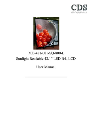
- 4. General Description 1.1 Features Resizing LCD Square Screen (8 : 9) High Brightness 800 nits Sunlight Readable LED Backlight Slim Bezel High Color Saturation BL MTBF: 100,000 hours (H),178°(V) Color Saturation (NTSC) 94% Display Colors 1.07G Response Time (Typical) 9.5ms Panel Interface V-by-One AD Board Input Interface VGA, DVI-D, HDMI, DP Input Power AC100~240V Power Consumption 150W OSD Key 5 Keys (Power Switch, Menu, +, Exit, -) OSD Control Brightness, Color, Contrast, Auto Turing, H/V Position…etc Dimensions (mm) 743.9 x 840.6 x 70.8 Bezel Size(U/B/L/R) 16.3/16.3/16.3/16.3 mm Weight (Net) 22 kg Mounting 400x300, 400x200 Operating Temperature 0 ˚C ~ 50 ˚C Storage Temperature -20 ˚C ~ 60 ˚C The MO-421-001-SQ-800-L is a 42.1 inch color TFT-LCD display with special aspect ratio 8:9 and wide resolution 1900 x 2160 with HCS (High Color Saturation). Designed for high brightness 800 nits with power efficiency LED backlight. It provides LCD panel with specific aspect ratios and sunlight readable for digital signage, public transportation, exhibition hall, department store, and vending machine. Description 42.1” Resizing LCD, 800 nits LED backlight, MaxRGB, 1900x2160 Screen Size 42.1” Display Area (mm) 706.8(H) x 803.5(V) Brightness 800 cd/m2 Resolution 1900x2160 Aspect Ratio 8 : 9 Contrast Ratio 7700 : 1 Pixel Pitch (mm) 0.372(H) x 0.372(V) Pixel Per Inch (PPI) 68 Viewing Angle 178° 1.2 General Specifications Model Name MO-421-001-SQ-800-L Panel + LED Driving Board + AD Control Board + Housing
- 5. 1.3 Absolute Maximum Ratings Permanent damage may occur if exceeding the following maximum rating. Note (1) Temperature and relative humidity range is shown in the figure below. (a) 90 %RH Max. (Ta ≦ 40 ºC). (b) Wet-bulb temperature should be 39 ºC Max. (c) No condensation. Note (2) Thermal management should be considered in final product design to prevent the surface temperature of display area from being over 65 ºC. The range of operating temperature may degrade in case of improper thermal management in final product design. Note (3) The rating of environment is base on LCD module. Leave LCD cell alone, this environment condition can’t be guaranteed. Except LCD cell, the customer has to consider the ability of other parts of LCD module and LCD module process.
- 6. Electrical Specifications 2.1 Electrical Characteristics Permanent damage may occur if exceeding the following maximum rating. Note (1) Permanent damage to the device may occur if maximum values are exceeded. Function operation should be restricted to the conditions described under Normal Operating Conditions. TFT LCD
- 7. Note (1) The module should be always operated within the above ranges. The ripple voltage should be controlled under 10% of Vcc (Typ.). Note (2) Measurement condition: Note (3) The specified power consumption and power supply current is under the conditions at Vcc = 12 V, Ta = 25 ±2 ºC, fv= 60 Hz, whereas a power dissipation check pattern below is displayed.
- 8. 2.2 Input Pin Assignment CNF1 Connector Pin Assignment (187059-51221(P-TWO), WF23-402-5133(FCN)) Matting connector : FI-RE51HL (JAE)
- 9. Note (1) V-by-One HS Data Mapping
- 10. Note (2) Input signal for Left Right eye frame synchronous Note (3) Local dimming enable selection. (Default: enable) L= Connect to GND, H=Connect to +3.3V or Open LD_EN enable pin should be set in power on stage. Backlight should be turned off in the period of changing original setting after power on.
- 11. Note (4) The definition of L/R_O signal as follows L= 0V , H= +3.3V Note (5) Interface optional pin has internal scheme as following diagram. Customer should keep the interface voltage level requirement which including Panel board loading as below. Note (6) Interface optional pin has internal scheme as following diagram. Customer should keep the interface voltage level requirement which including Panel board loading as below.
- 12. Note (7) V-by-One HS connector pin order defined as follows Note (8) V-by-One connector mating dimension range request is 0.93mm~1.0mm as below Note (9) Reserved for internal use. Please leave it open. Note (10)The detail setting such as I2C command or timing requirement in FHD/QFHD is specified application note. It’s important and necessary to follow the specification either in product SPEC or application note, otherwise it may lead to abnormalor no display. application note would be provided in the design-in stage.
- 13. Color Data input Assignment The brightness of each primary color (red, green and blue) is based on the 10-bit gray scale data input for the color. The higher the binary input the brighter the color. The table below provides the assignment of color versus data input. Note (1) 0: Low Level Voltage,1: High Level Voltage
- 14. 2.3 Interface Timing Input Signal Timing Specifications The input signal timing specifications are shown as the following table and timing diagram. (Ta = 25 ±2 ºC) Input Timing spec for QFHD Frame Rate = 50Hz Input Timing spec for QFHD Frame Rate = 60Hz
- 15. Input Timing Spec for FHD, Frame Rate = 50Hz Input Timing Spec for FHD, Frame Rate = 60Hz
- 16. Input Timing Spec for FHD, Frame Rate = 100Hz Input Timing Spec for FHD, Frame Rate = 120Hz
- 17. Input Timing spec for QFHD, Frame Rate = 24Hz Input Timing spec for QFHD, Frame Rate = 30Hz
- 18. Note (1) Please make sure the range of pixel clock has followthe below equation: Fclkin(max) ≧ Fr X Tv X Th Fr X Tv X Th ≧ Fclkin (min) Note (2) Intra-pair Data skew
- 19. Note (3) V-by-One HS Inter-pair skew. Note (4) The SSCG (Spread spectrum clock generator) is defined as below figures. Note (5) Please fix the Vertical timing (Vertical Total =TBD / Display = TBD / Blank = TBD) in 120Hz 3D mode Note (6) In 3D mode, the set up Fr6 in Typ. ±3 Hz .In order to ensure that the electric function performance to avoid no display symptom.(Except picture quality symptom.) Note (7) In 3D mode, the set up Tv and Tvb in Typ. ±30.In order to ensure that the electric function performance to avoid no display symptom.(Except picture quality symptom.) Note (8) The frame-to-frame jitter of the input frame rate is defined as the above figures. FRn = FRn-1 ±1.8%. Note (9) The setup of the frame rate jitter > 1.8% may result in the cosmetic LED backlight symptom but the electric function is not affected.
- 20. 2.4 V by One Input Signal Timing Diagram Table 1 Eye Mask Specification Note (1) Input levels of V-by-One HS signals are comes from “V-by-One HS Stander Ver.1.4”
- 21. Byte Length and Color mapping of V-by-One HS
- 22. 2.5 Power On/Off Sequence (Ta = 25 ±2 ºC) To prevent a latch-up or DC operation of LCD module, the power on/off sequence should be as the diagram below.
- 23. 2D/3D MODE CHANGE SIGNAL SEQUENCE WITHOUT VCC TURN OFF AND TURN ON
- 24. Note (1) The supply voltage of the external system for the module input should follow the definition of Vcc. Note (2) Apply the LED voltage within the LCD operation range. When the backlight turns on before the LCD operation or the LCD turns off before the backlight turns off, the display may momentarily become abnormal screen. Note (3) In case of Vcc is in off level, please keep the level of input signals on the low or high impedance. IfT2<0,that maybe cause electrical overstress failure. Note (4) T4 should be measured after the module has been fully discharged between power off and on period. Note (5) Interface signal shall not be kept at high impedance when the power is on. Note (6) When 2D/3D mode is changed, TCON will insert black pattern internally. During black insertion, TCON would load required optical table and TCON parameter setting. The black insertion time should be longer than 650ms because TCON must recognize 2D or 3D format and set the correct parameter. Note (7) Vcc must decay smoothly when power-off. Note (8) T5 > (T13 + T14) Note (9) T16, V-by-One signals shall be stabilized and follows timing specification which defined by section 6.1 &6.2. Note (10) T11 is at least 1600ms.It is also determined by the SOC stability time. If SOC would spend some time into stable state, T11 will be stable time plus 1600ms.
- 25. Optical Specification Item Symbol Condition Min. Typ. Max. Unit Note Color chromaticity Red Rx θx=0 θy=0 Klein K-10 0.652 0.682 0.712 - Test Mode: (1) (2) (3) Ry 0.273 0.303 0.333 - Green Gx 0.190 0.220 0.250 - Gy 0.650 0.680 0.710 - Blue Bx 0.114 0.144 0.174 - By 0.029 0.059 0.089 - White Wx 0.251 0.281 0.311 - Wy 0.263 0.293 0.323 - Center Luminance of White Lc θx=0 θy=0 BM-7 800 cd/m2 Uniform Lu 86 % Contrast Ratio CR θx=0 θy=0 Klein K-10 7700:1 - Test Mode: (1) (4)Color Saturation NTSC 94 % Viewing Angle Horizontal θx+ CR ≥ 10 89 Deg Test Mode: (1) (3) θx- 89 Vertical θy+ 89 θy- 89 Test Mode: (1) Definition of Viewing Angle (θx , θy):
- 26. (2) Definition of Test Point: BA C 2 1 3 Active Area (3) BM-7 Measurement Setup: (4) Klein K-10 Measurement Setup:
- 27. LED Driving Board Specifications This specification is applied to LED converter unit for LED backlight. 4.1 Operating Characteristics Item Symbol Conditions MIN. TYP. MAX. Unit Remark Input Voltage Vin 22 24 26 V Input Current (Low Brightness) IinL Vadj=5V 0.0 ----- ----- mA Input Current (High Brightness) IinH Vadj=0V 5.51 5.23 4.99 A (1) LED Current (Low Brightness) IoutL Vadj=5V 0.0 ----- ----- Arms LED Current (High Brightness) IoutH Vadj=0V 1.31 1.36 1.41 A J1~J4 1.31 1.36 1.41 A J5~J8 Working Frequency Freq Vadj=0V 350 400 450 KHz Brightness Control Vadj Connection of Voltage 0.2 ----- 4.8 V Vadj±5% ON/OFF Control Von Normal Operation 2 ----- 5 V Voff 0 ----- 0.8 V Output Voltage Vout Vadj=0V 41.3 41.8 42.3 V J1~J4 41.3 41.8 42.3 V J5~J8 Efficiency η Vadj=0V 89.3 90.6 91.8 % (2) Remark: (1) This data is based on the testing result of practical input voltage, Iin is measured by related Vin.(min, typ, max) (2) ηmax= Vout(max)*IoutH(max)/Vin(max)*IinH(min) ηmin= Vout(min)*IoutH (min)/Vin(min)*IinH(max)
- 28. 4.2 Connector Socket Input Connector: CN1(JST B10B-PH-K-S or Compatible) PIN No Symbol Description 1 Vin DC+ 2 Vin DC+ 3 Vin DC+ 4 Vin DC+ 5 Vin DC+ 6 GND Ground 7 GND Ground 8 GND Ground 9 GND Ground 10 GND Ground Input Connector: CN2(JST B3B-PH-K-S or Compatible) PIN No Symbol Description 1 Control ON/OFF Control 2 Brightness Brightness Control 3 GND Ground Output Connector: J1,J2,J5,J6 (JST S2B-EH or Compatible) PIN NO Symbol Description 1 Output LED High Voltage( + ) 2 Output LED Low Voltage ( - )
- 29. 4.3 Mechanical Characteristics Dimension: 160mm*90mm*12.5mm 12.5mm
- 32. AD9131GDHPAR Board & OSD Functions We developed this A/D board to support industrial high brightness and commercial applications. This A/D board has many functions. It has an external luminance sensor as an option, or optional VR button to control brightness, fan rotation and RS232. Rev.1 is European RoHS compliant. 6.1 General Description Max Resolution Up To UHD(4096X2160) Support V-By-one panel Analog RGB Input up to 205MHz DVI operates up to165M Hz 1 ULTRA-RELIABLE Dual-link DVI INPUT(4K2K@30Hz) 1 VGA INPUT(Optional) 1 HDMI(HDMI 2.0) Input(4K2K@60Hz) 1 Display port Input (DP 1.2a) (4K2K@60Hz) Support Panel DC5V or 3.3V, 12V Output External Fan Control by Software OSD Control Inverter Analog or PWM Dimming Control External V.R. brightness control (Optional) External light sensor brightness control (Optional) External RS232 control (Optional) Input Power 24Vdc,or 12Vdc(24Vdc Power Input Is Optional)
- 33. 6.2 Outline Dimensions AD9131GDHPAR 150mm x 100mm
- 34. 6.3 AD9131GDHPAR Board Pin Define
- 35. J10: Panel V-by-One connector Pin No. Function Pin No. Function 1 PANEL-VCC 27 GND 2 PANEL-VCC 28 RX0N 3 PANEL-VCC 29 RX0P 4 PANEL-VCC 30 GND 5 PANEL-VCC 31 RX1N 6 PANEL-VCC 32 RX1P 7 PANEL-VCC 33 GND 8 PANEL-VCC 34 RX2N 9 NC 35 RX2P 10 GND 36 GND 11 GND 37 RX3N 12 GND 38 RX3P 13 GND 39 GND 14 GND 40 RX4N 15 eDP_HPD1 41 RX4P 16 AUXTX_P1 42 GND 17 AUXTX_N1 43 RX5N 18 P_SDA 44 RX5P 19 P_SCL 45 GND 20 NC 46 RX6N 21 eDP_HPD0 47 RX6P 22 LD_EN 48 GND 23 AUXTX_P0 49 RX7N 24 AUXTX_N0 50 RX7P 25 HTPDN 51 GND 26 LOCKN CN5: DVI-D Input Connector (24pin ) Pin No. Function Pin No. Function Pin No. Function 1 T.M.D.S. Data2- 9 T.M.D.S. Data1- 17 T.M.D.S. Data0- 2 T.M.D.S. Data2+ 10 T.M.D.S. Data1+ 18 T.M.D.S. Data0+ 3 T.M.D.S. Data2/4 Shield 11 T.M.D.S Data1/3 Shield 19 T.M.D.S. Data0/5 Shield 4 T.M.D.S. Data4- 12 T.M.D.S. Data3- 20 T.M.D.S. Data5-
- 36. 5 T.M.D.S. Data4+ 13 T.M.D.S. Data3+ 21 T.M.D.S. Data5+ 6 DDC Clock 14 +5V Power 22 T.M.D.S. Clock Shield 7 DDC Data 15 Ground (for +5V) 23 T.M.D.S. Clock+ 8 Vertical SYNC. 16 Hot Plug Detect 24 T.M.D.S. Clock- CN2: Analog RGB Input connector (13pin connector) Pin No. Symbol Description Pin No. Symbol Description 1 SDA DDC Serial Data 8 BLUE_RTN Blue Return 2 SCL DDC Data Clock 9 BLUE Analog Blue 3 GND Reserved 1 0 GREEN_RTN Green Return 4 +5V +5VDDC 1 1 GREEN Analog Green 5 GND Reserved 1 2 RED_RTN Red Return 6 VSYNC Vertical Sync 1 3 RED Analog Red 7 HSYNC Horizontal Sync CN4: HDMI Connector (19pin HDMI) Pin No. Function Pin No. Function Pin No. Function 1 T.M.D.S. Data2+ 9 T.M.D.S. Data0- 17 GND 2 Shield 10 T.M.D.S. Clock+ 18 HDMI 5V 3 T.M.D.S. Data2- 11 Shield 19 Hot Plug Detect 4 T.M.D.S. Data1+ 12 T.M.D.S. Clock- - 5 Shield 13 CEC 6 T.M.D.S. Data1- 14 NC 7 T.M.D.S. Data0+ 15 HDMI_SCL 8 Shield Shield 16 HDMI_SDA CN8: HDMI Connector (18pin 2.0mm) Pin No. Function Pin No. Function Pin No. Function 1 T.M.D.S. Data2+ 9 T.M.D.S. Data0+ 17 HDMI_SCL 2 T.M.D.S. Data2- 10 T.M.D.S. Data0- 18 HDMI_SDA 3 Shield 11 Shield
- 37. 4 Shield 12 CEC 5 T.M.D.S. Data1+ 13 T.M.D.S. Clock+ 6 T.M.D.S. Data1- 14 T.M.D.S. Clock- 7 Shield 15 HDMI 5V 8 Shield Shield 16 Hot Plug Detect CN3: DISPLAY PORT Connector (20pin DP) Pin No. Function Pin No. Function 1 LAN_C_D3N 11 GND 2 GND 12 ML_LANE0_P 3 LAN_C_D3P 13 GND 4 ML_LANE2_N 14 GND 5 GND 15 AUX _CH_P 6 ML_LANE2_P 16 GND 7 ML_LANE1_N 17 AUX _CH_N 8 GND 18 Hot plug detect 9 ML_LANE1_P 19 GND 10 ML_LANE0_N 20 DP +5V CN1: Power DIN(24V or 12V) Pin No. Function Pin No. Function 1 24Vdc or 12Vdc(Not 1) 2 24Vdc or 12Vdc (Not 1) 3 GND 4 GND CN1: Power Jack (24V or 12V) Pin No. Function Pin No. Function 1 24Vdc or 12Vdc(Not 1) 2 GND 3 GND
- 38. J1: Power input connector (6 pin 2.0mm) Pin No. Function Pin No. Function 1 24Vdc or 12Vdc(Not 1) 2 24Vdc or 12Vdc(Not 1)3 24Vdc or 12Vdc(Not 1) 4 GND 5 GND 6 GND Not 1:Power input has tow different versions,12V power input version and 24V input version don’t mistake. CN7: Power out connector (5V/12V)(4PIN 2.0mm) Pin No. Function Pin No. Function 1 5Vdc 2 GND 3 12Vdc 4 GND J11: Inverter Connector (8PIN 2.0mm) Pin No. Symbol Description Pin No. Symbol Description 1 ON/OFF Backlight ON/OFF 5 GND GND 2 BRIGHT Dimming adjust 6 12VDC Input 12VDC 3 GND GND 7 12VDC Input 12VDC 4 GND GND 8 12VDC Input 12VDC J13,J12: FAN (2PIN 2.0mm) Pin No. Function Pin No. Function 1 FAN(+) 2 GND J2: Key Pad (9PIN 2.0mm) Pin No. Function Pin No. Function 1 POWER KEY 6 MENU KEY 2 GREEN LED 7 AUTO KEY 3 RED LED 8 GND 4 DOWN KEY 9 GND 5 UP KEY J5: VR connector (3PIN 2.0mm) Pin No. Function Pin No. Function 1 3,3VDC 2 VR OUT 3 GND
- 39. J4: Ambient (2PIN 2.0mm) Pin No. Function Pin No. Function 1 3.3VDC/5VDC 2 Sensor Out JP1: PANEL VCC (3PIN 2.54mm) Pin No. Function Pin No. Function 1-2 12V 5-6 3.3V 3-4 5V J8 & J9: Speaker Connector (2PIN 2.0mm) Pin No. Function Pin No. Function 1 SPK+ 2 SPK- J13 UART Connector (RS232 IN) (3PIN 2.0mm) Pin No. Function Pin No. Function 1 TXD 2 RXD 3 GND J4: SPDIF (2PIN 2.0mm) Pin No. Function Pin No. Function 1 SPDIF_OUT 2 GND JP2: EDID (2PIN 2.0mm) Pin No. Function Pin No. Function 1 EEROM Write protect 2 GND When need to rewrite EEROM EDID , short two pin .
- 40. 6.4 OSD Function MEMBRANE CONTROL BUTTOM Key: (Power) function key Press the power switch will turn the monitor on. Press it again to turn the monitor off. LED Status: Power ON-Green / Power off-No. Key: (Menu + Selection Right + Enter) function key Press this button to the OSD “main menu”. And then press this button go to the “Selection Right” function, and press again this button to “Enter”. Key: (Menu + Selection Up + Increase) function key Press this button to the OSD “main menu”. And then press this button go to the “Selection Up” function, and press again this button to adjustment value “Increase”. Key: (Menu + Exit) function key Enter to the OSD adjustment menu. It also used for go back to previous menu for sub-menu. Key: (Menu + Selection Down + Decrease) function key Press this button to the OSD “main menu”. And then press this button go to the “Selection Down” function, and press again this button to adjustment value “Decrease”.
- 41. Screen Adjustment Operation Procedure 1. Entering the screen adjustment The setting switches are normally at stand-by. Push the Menu Key once to display the main menu of the screen adjustment. The adjustable items will be displayed in the main menu. 2. Entering the settings Use the Down Key and Up Key buttons to select the desired setting icon and push the SELECT button to enter sub-menu. 3. Change the settings After the sub-menu appears, use the Down Key and Up Key buttons to change the setting values. 4. Save After finishing the adjustment, push the button to memorize the setting. 5. Return & Exit the Main Menu Exit the screen adjustment; push the “MENU” button. When no operation is done around 30 sec (default OSD timeout), it goes back to the stand-by mode and no more switching is accepted except MENU to restart the setting. 6.5 OSD Menu By pressing the “menu” button, you will see the below picture. Across from timing you will see resolution, frequency, and V-frequency of the panel. These cannot be altered by the user.
- 42. Precautions 7.1 Handling Precautions (1) The module should be assembled into the system firmly by using every mounting hole. Be careful not to twist or bend the module. (2) While assembling or installing modules, it can only be in the clean area. The dust and oil may cause electrical short or damage the polarizer. (3) Use fingerstalls or soft gloves in order to keep display clean during the incoming inspection and assembly process. (4) Do not press or scratch the surface harder than a HB pencil lead on the panel (5) because the polarizer is very soft and easily scratched. (6) If the surface of the polarizer is dirty, please clean it by some absorbent cotton or soft cloth. Do not use Ketone type materials (ex. Acetone), Ethyl alcohol, Toluene, Ethyl acid or Methyl chloride. It might permanently damage the polarizer due to chemical reaction. (7) Wipe off water droplets or oil immediately. Staining and discoloration may occur if (8) they left on panel for a long time. (9) If the liquid crystal material leaks from the panel, it should be kept away from the eyes or mouth. In case of contacting with hands, legs or clothes, it must be washed away thoroughly with soap. (10) Protect the module from static electricity, it may cause damage to the C-MOS Gate Array IC. (11) Do not disassemble the module. (12) Do not pull or fold the lamp wire. (13) Pins of I/F connector should not be touched directly with bare hands. 7.2 Storage Precautions (1) High temperature or humidity may reduce the performance of module. Please store LCD module within the specified storage conditions. (2) It is dangerous that moisture come into or contacted the LCD module, because the moisture may damage LCD module when it is operating. (3) It may reduce the display quality if the ambient temperature is lower than 10 ºC. For example, the response time will become slowly, and the starting voltage of lamp will be higher than the room temperature. 7.3 Operation Precautions (1) Do not pull the I/F connector in or out while the module is operating. (2) Always follow the correct power on/off sequence when LCD module is connecting and operating. This can prevent the CMOS LSI chips from damage during latch-up. Disclaimer All information in this document are subject to change, please constant LiteMax for any new design.