Más contenido relacionado
La actualidad más candente (20)
Similar a LEC20G604 (6).pdf (20)
LEC20G604 (6).pdf
- 1. ©2011 LSIS, Preliminary Rev 0.1_07.04.2011 1 of 15
LEC20G604
SISPM™
600V 20A PIM(CIB) IGBT Module
Features Preliminary Data
• Trench Field Stop technology IGBT adopted
• Low saturation voltage
• Positive temperature coefficient
• Fast switching
• Free wheeling diodes with fast and soft reverse recovery
• Industrial standard package with insulated substrate
• Temperature sensor included
• Input from single or three phase grid
• Dynamic braking operation
Applications
• Three phase synchronous or asynchronous motor drive
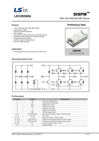
Internal Equivalent Circuit
Pin Description
Pin Number Pin Name Pin Description
1 GB Gate Input for Braking IGBT
2 EB Emitter Input for Braking IGBT
3 DCN Negative DC Link Input
4 DCP Positive DC Link Intput
5 P Positive DC Link Output
6 N Negative DC Link Output
7 COM Common Supply Ground
8, 9,10 GUN, GVN, GWN Gate Input for Low-side U Phase, V Phase, W Phase
11, 12 TH1, TH2 NTC-, NTC+
13, 14, 15 U, V, W Output for U Phase, V Phase, W Phase
16, 18, 20 EWP, EVP, EUP Emitter Input for High-side W Phase, V Phase, U Phase
17, 19, 21 GWP, GVP, GUP Gate Input for High-side W Phase, V Phase, U Phase
22, 23, 24 R, S, T Input for R Phase, S Phase, T Phase
25 B Output for Braking
SISPM1
82.2 x 37.9 x 21.7mm
- 2. LEC20G604
2 of 15 ©2011 LSIS, Preliminary Rev 0.1_07.04.2011
Absolute Maximum Ratings TC = 25°C unless otherwise noted
(Note *1) The Maximum junction temperature of chip is 150 °C.
(Note *2) The Maximum junction temperature of chip is 175 °C.
Item Symbol Parameter Conditions Value Units
Input
Rectifier
VRRM Repetitive Peak Reverse Voltage 1600 V
IFAV Forward Current per Diode @ Tj = 150 °C, TC = 80 °C 20 A
IFSM Surge Forward Current (Chip level) @ tP = 10 ms, half sine wave 220 A
I2
t I2
t - Value (Chip level) @ tP = 10 ms, half sine wave 200 A2
s
PD Maximum Power Dissipation @ Tj = 150 °C, TC = 80 °C 40 W
Tj Operating Junction Temperature *(1) - -40 ~ 125 °C
Transistor
Inverter
VCES Collector-Emitter Breakdown Voltage - 600 V
VGES Gate-Emitter Peak Voltage - ± 20 V
IC DC Collector Current @ Tj = 175 °C, TC = 80 °C 20 A
Icpulse Repetitive Peak Collector Current @ tP = 1 ms 40 A
PD Maximum Power Dissipation @ Tj = 175 °C, TC = 80 °C 50 W
TSC SC Withstand Time (Chip level) VGE = 15 V, VCE = 300 V 5 μs
Tj Operating Junction Temperature *(2) - -40 ~ 125 °C
Diode
Inverter
VRRM Repetitive Peak Reverse Voltage - 600 V
IF DC Forward Current @ Tj = 175 °C,TC = 70 °C 20 A
IFRM Repetitive Peak Forward Current @ tP = 1 ms 40 A
PD Maximum Power Dissipation @ Tj = 175 °C, TC = 70 °C 40 W
Tj Operating Junction Temperature *(2) - -40 ~ 125 °C
Transistor
Brake
VCES Collector-Emitter Breakdown Voltage - 600 V
VGES Gate-Emitter Peak Voltage - ± 20 V
IC DC Collector Current @ Tj = 175 °C, TC = 80 °C 20 A
Icpulse Repetitive Peak Collector Current @ tP = 1 ms 40 A
PD Maximum Power Dissipation @ Tj = 175 °C, TC = 80 °C 45 W
TSC SC Withstand Time (Chip level) @ VGE = 15 V, VCE = 300 V 5 μs
Tj Operating Junction Temperature *(2) - -40 ~ 125 °C
Diode
Brake
VRRM Repetitive Peak Reverse Voltage - 600 V
IF DC Forward Current @ Tj = 175 °C, TC = 70 °C 20 A
IFRM Repetitive Peak Forward Current @ tP = 1 ms 40 A
PD Maximum Power Dissipation @ Tj = 175 °C, TC = 70 °C 40 W
Tj Operating Junction Temperature *(2) - -40 ~ 125 °C
Module
Tstg Storage Temperature - -40~125 °C
Viso Isolation Voltage @ AC 1minute 2500 V
W Weight - 50 g
- 3. LEC20G604
©2011 LSIS, Preliminary Rev 0.1_07.04.2011 3 of 15
Electrical Characteristics TC = 25°C unless otherwise noted
Input Rectifier Characteristics
Transistor-Inverter Characteristics
Diode-Inverter Characteristics TC = 25°C unless otherwise noted
Transistor- Brake Characteristics
Symbol Parameter Conditions Min Typ Max Units
VF Diode Forward Voltage
TC = 25 °C, IF = 20 A - 1.2 - V
TC = 125 °C, IF = 20 A - 1.1 - V
Vto Threshold Voltage TC = 125 °C - 0.83 - V
IR Reverse Current (Chip level) TC = 25 °C, VRRM = 300 V - 0.1 - mA
rt Slope Resistance TC = 125 °C - 20.8 - mΩ
Rth(J-C) Thermal Resistance (IGBT Part) Junction-to-Case - 1.3 - °C/W
Symbol Parameter Conditions Min Typ Max Units
VGE(th) Gate-Emitter threshold Voltage VCE = VGE, ICE = 20mA - 5.6 - V
VCE(sat) Collector-Emitter Saturation Voltage
TC = 25 °C, ICE = 20 A, VGE = 15 V - 1.9 - V
TC = 125 °C, ICE = 20 A, VGE = 15 V - 2.3 - V
ICES Collector-Emitter Cut-off Current VGE = 0 V, VCE = 300 V - - 250 μA
ICES Gate-Emitter Leakage Current VGE = ± 20 V, VCE = 0 V - - - A
Ciss Input Capacitance VCE = 50 V, VGE = 0 V
f = 100 kHz, TC = 25 °C
(Chip level)
- - - nF
Coss Output Capacitance - - - nF
Crss Reverse Transfer Capacitance - - - nF
td(on) Turn-On Delay Time
TC = 125 °C, RG ON = 50 Ω
RG OFF = 25 Ω, L = 500 μH
VCE = 300 V, VGE = 0 V~15 V
ICE = 20 A
- 67 - ns
tr Rise Time - 52 - ns
td(off) Turn-Off Delay Time - 138 - ns
tf Fall Time - 37 - ns
Eon Turn-On Switching Loss - 0.69 - mJ
Eoff Turn-Off Switching Loss - 0.28 - mJ
Ets Total Switching Loss - 0.97 - mJ
QG Total Gate Charge
VGE = 0 V ~ 15 V
- 56 - nC
QGE Gate-Emitter Charge - 23 - nC
QGC Gate-Collector Charge - 15 - nC
Rth(J-C) Thermal Resistance (IGBT Part) Junction-to-Case 1.5 - °C/W
Symbol Parameter Conditions Min Typ Max Units
VF Diode Forward Voltage IF = 20 A, VGE = 0 V TC = 125 °C - 1.7 - V
trr Diode Reverse Recovery Time RG ON = 50 Ω
L = 500 μH
VCE = 300 V
VGE = 0 V~15 V
ICE = 20 A
TC = 125 °C - 465 - ns
IRRM Diode Peak Reverse Recovery Current TC = 125 °C - 19 - A
Qrr Diode Reverse Recovery Charge TC = 125 °C - 2.3 - μC
Err Diode Reverse Recovery Energy TC = 125 °C - 0.48 - mJ
Rth(J-C) Thermal Resistance (IGBT Part) Junction-to-Case - 2.1 - °C/W
Symbol Parameter Conditions Min Typ Max Units
VGE(th) Gate-Emitter threshold Voltage VCE = VGE, ICE = 20mA - 5.6 - V
VCE(sat) Collector-Emitter Saturation Voltage
TC = 25 °C, ICE = 20 A, VGE = 15 V - 1.9 - V
TC = 125 °C, ICE = 20 A, VGE = 15 V - 2.3 - V
ICES Collector-Emitter Cut-off Current VGE = 0 V, VCE = 300 V - - 250 μA
ICES Gate-Emitter Leakage Current VGE = ± 20 V, VCE = 0 V - - - A
Ciss Input Capacitance VCE = 50 V, VGE = 0 V
f = 100 kHz, TC = 25 °C
(Chip level)
- - - nF
Coss Output Capacitance - - - nF
Crss Reverse Transfer Capacitance - - - nF
- 4. LEC20G604
4 of 15 ©2011 LSIS, Preliminary Rev 0.1_07.04.2011
Diode-Brake Characteristics TC = 25°C unless otherwise noted
NTC thermister Characteristics
* This specifications may not be considered as an assurance of characteristics and may not have same characteristics.
in case of using different test systems from @LSIS. We therefore strongly recommend prior consultation of our engineers.
td(on) Turn-On Delay Time
TC = 125 °C, RG ON = 50 Ω
RG OFF = 25 Ω, L = 500 μH
VCE = 300 V, VGE = 0 V~15 V
ICE = 20 A
- 58 - ns
tr Rise Time - 57 - ns
td(off) Turn-Off Delay Time - 145 - ns
tf Fall Time - 19 - ns
Eon Turn-On Switching Loss - 0.71 - mJ
Eoff Turn-Off Switching Loss - 0.25 - mJ
Ets Total Switching Loss - 0.96 - mJ
QG Total Gate Charge
VGE = 0 V ~ 15 V
- 56 - nC
QGE Gate-Emitter Charge - 23 - nC
QGC Gate-Collector Charge - 15 - nC
Rth(J-C) Thermal Resistance (IGBT Part) Junction-to-Case 1.6 - °C/W
Symbol Parameter Test Conditions Min Typ Max Units
VF Diode Forward Voltage IF = 20 A, VGE = 0 V TC = 125 °C - 1.7 - V
trr Diode Reverse Recovery Time RG ON = 50 Ω
L = 500 μH
VCE = 300 V
VGE = 0 V~15 V
ICE = 20 A
TC = 125 °C - 485 - ns
IRRM Diode Peak Reverse Recovery Current TC = 125 °C - 15 - A
Qrr Diode Reverse Recovery Charge TC = 125 °C - 2.1 - μC
Err Diode Reverse Recovery Energy TC = 125 °C - 0.48 - mJ
Rth(J-C) Thermal Resistance (IGBT Part) Junction-to-Case - 2.1 - °C/W
Symbol Parameter Test Conditions Min Typ Max Units
R25 Resistance TC = 25 °C - 4.7 - kΩ
P Power TC = 25 °C - 210 - mW
B25/100 B Constant TC = 25 °C, ± 3% tolerance - 3650 - K
Symbol Parameter Conditions Min Typ Max Units
- 5. LEC20G604
©2011 LSIS, Preliminary Rev 0.1_07.04.2011 5 of 15
Input rectifier
Fig 1. Typical Diode Forward Characteristics Fig 2. Case Temperature vs. Forward Current
Fig 3. Typical Diode Thermal Impedance
- 6. LEC20G604
6 of 15 ©2011 LSIS, Preliminary Rev 0.1_07.04.2011
Transistor-inverter/Diode-Inverter
Fig 4. Typical IGBT Output Characteristics Fig 5. Typical IGBT Output Characteristics
Fig 6. Typical IGBT Output Characteristics Fig 7. Typical Diode Forward Characteristics
Fig 8. Typical Switching Time vs. Collector Current Fig 9. Typical Switching Time vs. Collector Current
- 7. LEC20G604
©2011 LSIS, Preliminary Rev 0.1_07.04.2011 7 of 15
Transistor-inverter/Diode-Inverter
Fig 10. Typical Switching Time vs. Gate Resistor Fig 11. Typical Switching Time vs. Gate Resistor
Fig 12. Typical IGBT Switching Loss Fig 13. Typical IGBT Switching Loss
Fig 14. Typical Recovery Characteristics of Diode Fig 15. Typical Recovery Characteristics of Diode
- 8. LEC20G604
8 of 15 ©2011 LSIS, Preliminary Rev 0.1_07.04.2011
Transistor-inverter/Diode-Inverter
Fig 16. Typical Recovery Characteristics of Diode Fig 17. Typical Recovery Characteristics of Diode
Fig 18. Typical Diode Switching Loss Fig 19. Typical Diode Switching Loss
Fig 20. Typical Gate Charge Characteristics Fig 21. Case Temperature vs. Collector Current
- 9. LEC20G604
©2011 LSIS, Preliminary Rev 0.1_07.04.2011 9 of 15
Transistor-inverter/Diode-Inverter
Fig 22. Case Temperature vs. Forward Current Fig 23. Typical IGBT Thermal Impedance
Fig 24. Typical Diode Thermal Impedance
- 10. LEC20G604
10 of 15 ©2011 LSIS, Preliminary Rev 0.1_07.04.2011
Transistor-Brake/Diode-Brake
Fig 25. Typical IGBT Output Characteristics Fig 26. Typical IGBT Output Characteristics
Fig 27. Typical IGBT Output Characteristics Fig 28. Typical Diode Forward Characteristics
Fig 29. Typical Switching Time vs. Collector Current Fig 30. Typical Switching Time vs. Collector Current
- 11. LEC20G604
©2011 LSIS, Preliminary Rev 0.1_07.04.2011 11 of 15
Transistor-Brake/Diode-Brake
Fig 31. Typical Switching Time vs. Gate Resistor Fig 32. Typical Switching Time vs. Gate Resistor
Fig 33. Typical IGBT Switching Loss Fig 34. Typical IGBT Switching Loss
Fig 35. Typical Recovery Characteristics of Diode Fig 36. Typical Recovery Characteristics of Diode
- 12. LEC20G604
12 of 15 ©2011 LSIS, Preliminary Rev 0.1_07.04.2011
Transistor-Brake/Diode-Brake
Fig 37. Typical Recovery Characteristics of Diode Fig 38. Typical Recovery Characteristics of Diode
Fig 39. Typical Diode Switching Loss Fig 40. Typical Diode Switching Loss
Fig 41. Typical Gate Charge Characteristics Fig 42. Case Temperature vs. Collector Current
- 13. LEC20G604
©2011 LSIS, Preliminary Rev 0.1_07.04.2011 13 of 15
Transistor-Brake/Diode-Brake
Fig 43. Case Temperature vs. Forward Current Fig 44. Typical IGBT Thermal Impedance
Fig 45. Typical Diode Thermal Impedance
- 14. LEC20G604
14 of 15 ©2011 LSIS, Preliminary Rev 0.1_07.04.2011
NTC
Fig 46. Typical NTC Characteristics