
Recomendados
Más contenido relacionado
La actualidad más candente
La actualidad más candente (20)
Similar a Programmable logic array
Similar a Programmable logic array (20)
Más de Huba Akhtar
Último
Último (20)
Programmable logic array
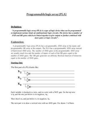
- 1. Programmablelogicarray(PLA) Definition: “A programmable logic array (PLA) is a type of logic device that can be programmed to implement various kinds of combinational logic circuits. The device has a number of AND and OR gates which are linked together to give output or further combined with more gates or logic circuits”. Explanation: A programmable logic array (PLA) has a programmable AND array at the inputs and programmable OR array at the outputs. The PLA has a programmable AND array instead of hard-wired AND array. The number of AND gates in the programmable AND array are usually much less and the number of inputs of each of the OR gates equal to the number of AND gates. The OR gate generates an arbitrary Boolean function of minterms equal to the number of AND gates. Starting Out: The first part of a PLA looks like: Each variable is hooked to a wire, and to a wire with a NOT gate. So the top wire is x2 and the one just below is its negation, x2. Then there's x1 and just below it, its negation, x1. The next part is to draw a vertical wire with an AND gate. I've drawn 3 of them.
- 2. Let's try to implement a truth table with a PLA. x2 x1 x0 z1 z0 0 0 0 0 0 0 0 1 1 0 0 1 0 0 0 0 1 1 1 0 1 0 0 1 1 1 0 1 0 0 1 1 0 0 0 1 1 1 0 1 Each of the vertical lines with an AND gate corresponds to a minterm. For example, the first AND gate (on the left) is the minterm: x2x1x0. The second AND gate (from the left) is the minterm: x2x1x0. The third AND gate (from the left) is the minterm: x2x1x0. I've added a fourth AND gate which is the minterm: x2x1x0.
- 3. The first three minterms are used to implement z1. The third and fourth minterm are used to implement z0. This is how the PLA looks after we have all four minterms. Now you might complain. How is it possible to have a one input AND gate? How can three inputs be hooked to the same wire to an AND gate? Isn't that invalid for combinational logic circuits? That's true, it is invalid. However, the diagram is merely a simplification. I've drawn the each of AND gate with three input wires, which is what it is in reality (there is as many input wires as variables). For each connection (shown with a black dot), there's really a separate wire. We draw one wire just to make it look neat.
- 4. The vertical wires are called the AND plane. We often leave out the AND gates to make it even easier to draw. We then add OR gates using horizontal wires, to connect the minterms together. Example:
- 5. Advantages of PLA: There is no need for the time-consuming logic design of random-logic gate networks and even more time-consuming layout. Design checking is easy, and design change is also easy. Layout is far simpler than that for random-logic gate networks, and thus is far less time-consuming. When new IC fabrication technology is introduced, we can use previous design information with ease but without change, making adoption of the new technology quick and easy. Only the connection mask needs to be custom-made. Disadvantages of PLA: Random-logic gate networks have higher speed than PLAs or ROMs. Random-logic gate networks occupy smaller chip areas than PLAs or ROMs, although the logic design and the layout of random-logic gate networks are far more tedious and time- consuming. Also, with large production volumes, random-logic gate networks are cheaper than PLAs or ROMs. Applications of PLAs: Considering the above advantages and disadvantages, PLAs have numerous unique applications. A micro- processor chip uses many PLAs because of easy of design change and check. In particular, PLAs are used in its control logic, which is complex and requires many changes, even during its design. Also, PLAs are used for code conversions, microprogram address conversions, decision tables, bus priority resolvers, and memory overlay.
- 6. Combinationallogiccircuit In digital circuit theory, combinational logic (sometimes also referred to as time- independent logic[1] ) is a type of digital logic which is implemented by Boolean circuits, where the output is a pure function of the present input only. This is in contrast to sequential logic, in which the output depends not only on the present input but also on the history of the input. In other words, sequential logic has memory while combinational logic does not. Combinational logic is used in computer circuits to perform Boolean algebra on input signals and on stored data. Practical computer circuits normally contain a mixture of combinational and sequential logic. For example, the part of an arithmetic logic unit, or ALU, that does mathematical calculations is constructed using combinational logic. Other circuits used in computers, such as half adders, full adders, half subtractors, full subtractors, multiplexers, demultiplexers, encoders and decoders are also made by using combinational logic.. SequentialLogicCircuit n digital circuit theory, sequential logic is a type of logic circuit whose output depends not only on the present value of its input signals but on the sequence of past inputs, the input history.[1][2][3][4] This is in contrast to combinational logic, whose output is a function of only the present input. That is, sequential logic has state (memory) while combinational logic does not.
- 7. Sequential logic is used to construct finite state machines, a basic building block in all digital circuitry. Virtually all circuits in practical digital devices are a mixture of combinational and sequential logic. A familiar example of a device with sequential logic is a television set with "channel up" and "channel down" buttons.[1] Pressing the "up" button gives the television an input telling it to switch to the next channel above the one it is currently receiving. If the television is on channel 5, pressing "up" switches it to receive channel 6. However, if the television is on channel 8, pressing "up" switches it to channel "9". In order for the channel selection to operate correctly, the television must be aware of which channel it is currently receiving, which was determined by past channel selections.[1] The television stores the current channel as part of its state. When a "channel up" or "channel down" input is given to it, the sequential logic of the channel selection circuitry calculates the new channel from the input and the current channel. DifferencebetweenCombinational&SequentialCircuits
- 8. Combinational Logic Circuits Sequential Logic Circuits Output is a function of the present inputs (Time Independent Logic). Output is a function of clock, present inputs and the previous states of the system. Do not have the ability to store data (state). Have memory to store the present states that is sent as control input (enable) for the next operation. It does not require any feedback. It simply outputs the input according to the logic designed. It involves feedback from output to input that is stored in the memory for the next operation. Used mainly for Arithmetic and Boolean operations. Used for storing data (and hence used in RAM). Logic gates are the elementary building blocks. Flip flops (binary storage device) are the elementary building unit. Independent of clock and hence does not require triggering to operate. Clocked (Triggered for operation with electronic pulses). Example: Adder [1+0=1; Dependency only on present inputs i.e., 1 and 0]. Example: Counter [Previous O/P +1=Current O/P; Dependency on present input as well as previous state]. References: https://www.techopedia.com/definition/12131/programmable-logic-array-pla https://courses.cs.washington.edu/courses/cse370/99sp/lectures/03- CombImpl/sld048.htm https://en.wikipedia.org/wiki/Combinational_logic https://en.wikipedia.org/wiki/Sequential_logic http://www.vlsifacts.com/difference-combinational-sequential-logic-circuits/