SlideShare una empresa de Scribd logo
1 de 56
Descargar para leer sin conexión
Chapter 4
Crystal Structures
Mr. Pem PHAKVISETH
pempvs@gmail.com
Department of Materials Science and Engineering
Souphanouvong University
Faculty of Engineering
1
Objective of Learning
• Describe crystal structure and arrangement of atoms in crystal structure,
formation of microstructure
• Recognizing the relationship between atomic bonding, crystal structure
and material properties
• Describes the X-Ray Diffraction
2
4.1 Crystal
3
• A crystal or crystalline solid is a solid material whose constituents (such as atoms,
molecules, or ions) are arranged in a highly ordered microscopic structure, forming a
crystal lattice that extends in all directions
Materials and Arrangement
The materials are arranged into Crystalline
• The atoms have an orderly arranged in a 3D .
• a sample: metal, ceramic ,some polymers
Long range order
The materials are arranged into Amorphous
• The atoms have an not order arrangement.
• Occurs for : Complex structure, fast cooling
Short range order
“Amorphous” = Non-crystalline
4
Energy and Arrangement
• Non dense, random packing
• Dense, ordered packing
The ordered packing is Dense, the structure will have lower energy. 5
Unit Cell
• Unit Cell : Is the unit of the smallest basic structure of a crystal or a specific unit that
produces crystal structure that can simulate the arrangement of atoms both crystals and
has a definite shape
• That will consist of atoms which is in a specific position within that cell
6
Space Lattice or Crystal Lattice
• So the word Crystal Lattice or Space Lattice therefore referring to the shape
formed by the arrangement of unit cells in 3 dimensions. When looking at each
dimension, it will look like all similar meshes.
• Lattice referring to the Network (lattice)
• Any complete crystal consists of a number of unit cells arranged in 3D, which we
call “Crystal Lattice or Space Lattice”.
7
Lattice Parameter
• Lattice Parameter : The distance or size of the unit cell of each side
• When changing to 3D on each side and the direction of the lattice parameter, it
must be able to fit into the 3D structure without any space remaining.
• a, b, c Is the distance or size of
Lattice Parameter
8
Crystalline Solid Formation
How do crystals occur?
• All materials are formed by the binding of atoms by bonds such as ionic, covalent
or metallic bonding.
• Crystalline solid, like metals, ceramics and some polymers.
• A non-crystalline solid is called a non-crystalline solid or amorphous, which is just
a group of atoms. Or molecules without certain structures
9
Mechanism of Crystallization
• In metals that are in a molten state the binding of atoms will have a sequence
short range order or disordered.
• The bonding and separation of atoms is random and can occur at any time.
Due to the high activation energy (due to high temperatures)
10
• There are two types of energy of atoms:
- Kinetic Energy is the energy related to the speed at which the atoms move
and vary directly with the temperature
- Potential energy is the energy that accumulates within when the atoms are
apart will have more energy of this type
• In a liquid state toms have higher energy values
11
• When the temperature drops below the hardness of that metal And begin to change to
solid state, the energy will be lower
• Atoms must emit latent heat called "Latent heat of fusion" in order to bond between
atoms to form a nuclei formation and grow into the nucleus and become atoms.
12
• Then the nucleus formed to become an atom And each atom comes together From the
incorporation of only a few atoms will begin to expand by holding on to the next
atom at all times Three-dimensional lattice arrangement with a certain distance and
position of atoms along the crystal axis
13
• The crystals will keep growing. And stop growing when colliding with other crystals
of different atomic directions the crystals that stop growing and are called “Grain”
• The seam that crystallizes connect with other crystals is called “grain boundary”
• After that, many grains combine to form a solid. And will be called as
“Polycrystalline Solid”
14
15
Grain growth
See VDO-Grain Growth
grain
grain
grain
intergranular
https://www.youtube.com/watch?v=FlkrBSh4514
How many types of atoms can be arranged in solid state?
• There are 7 systems of crystal systems based on the symmetry of the shape.
• Each crystal system can be further divided into 14 crystal structures according to the
arrangement of atoms.
• There 32 point group and 230 space group.
• The crystal structure is closely related to the properties such as strength, heat
resistance. Difficulty in forming, etc.
16
4.2 Crystal Structure Systems of Materials
Crystal System & Unit Cell Lattice Parameters
17
• Cubic system
• For other crystal structures
18
19
Is the length of the body
The angle value of the ideal angle between the axes
20
4.3 Crystal Structure Systems of Metals
There are 3 common crystal structures of metals
• Body Centered Cubic Structure (BCC)
• Face Centered Cubic Structure (FCC)
• Hexagonal Close Packed Structure (HCP)
21
1. Body Centered Cubic Structure (BCC)
• Found in Chromium, Lithium, Iron and Tungsten etc.
• have 1 atom in the middle And arranged in a straight
line diagonally with the atoms in all 8 angles and
connected throughout the crystal
• The direction in which the atoms are packed the most
is Diagonal line of the cube
22
Determined
a = lattice constant and
R = atomic radius
Will get a relationship
Number of atoms 1 unit cell
• All Angles 8 = (1/8) x 8 = 1 atom
• Center point = 1 atom
• Total 2 atom/unit cell
23
Example
24
2. Face Centered Cubic Structure(FCC)
• Found in copper, aluminum, silver and gold etc.
• Will have atoms in all 8 corners and at the center point
on all 6 sides
• The direction in which the atoms are compressed most
is the diagonal of each of the 6 sides of the cube.
25
from unit cell atoms will touch each
other diagonally of the side will
Number of atom 1 unit cell
• All angles 8 = (1/8) x 8 = 1 atom
• All side 6 = (1/2) x 6 = 3 atom
• Total 4 atom/unit cell
26
Diagonal side is equal to
Example
27
28
3. Hexagonal-Close Packed (HCP)
• Found in Magnesium, Titanium and Zinc etc.
• The top and bottom planes have atoms close together
to form a hexagon. And the central point of the plane
The middle plane will have 3 atoms.
• For ideal hcp , c/a = 1.633
1 Unit cell of HCP have 6 atom
29
1 Unit cell of HCP have 6 atom
• Middle atom = 3 atom
• Top-bottom atom = (1/2) x 2 = 1 atom
• Atoms at the corner = (1/6) x 12 = 2 atom
Cut times 1 remaining (1/2)
Cut times 2 remaining (1/3) X (1/2) = (1/6)
30
31
4.3 Atomic Packing Factor (APF)
• Is the value that tells the volume of the atom in unit cell
• Assuming the shape of a circle of atoms so.
𝑨𝑷𝑭 =
𝑽𝒐𝒍𝒖𝒎𝒆 𝒐𝒇 𝒂𝒕𝒐𝒎 𝒊𝒏 𝒖𝒏𝒊𝒕 𝒄𝒆𝒍𝒍
𝒗𝒐𝒍𝒖𝒎𝒆 𝒐𝒇 𝒖𝒏𝒊𝒕 𝒄𝒆𝒍𝒍
• In BCC, APF = 0.68
• In FCC and HCP, APF=0.74
32
Example of finding the Atomic Packing Factor for FCC
Close – packed directions:
Length = 4R
= 2𝑎
Unit cell Contain:
6 × 1/2 + 8 × 1/8= 4 atom/ unit cell
33
Example of finding the Atomic Packing Factor for FCC
• The FCC structure in 1 cell has 4 atoms.
• The volume of atoms is equal to (4/3) 𝜋𝑟3
• The volume of cell is equal to 𝑎3
34
4.4 Calculation to Density Computation of unit cell
Theoretical density calculation
Metal density (𝜌) can be calculated from take the mass of all the atoms, divided by the volume
of 1 unit cell
If the mass of atoms, A unit is atom mass unit (amu) to be divided by the Avogadro number
(6.023 × 10²³
𝑎𝑡𝑜𝑚𝑠/𝑚𝑜𝑙) In order to get the atomic mass 𝑀 𝑎𝑡𝑜𝑚
35
36
37
Density of different types of materials
Metals
• Compact structure (Metallic bonding)
• Very precious atomic mass
Ceramics
• Less compact structure(Covalent bonding)
• Is usually a lighter element
Polymers
• Very compact structure(Usually an allotrope)
• Is a very rare element (C,H,O)
composites
• Have medium properties
38
Example
39
4.5 Crystallographic Directions
• Is a vector indicating the direction in a crystal, used instead by [u,v,w] Which will be the
full number (integer number) The smallest (Projection) of core x, y and z in unit cell.
• Negative direction There will be a stroke above such as [ത100] Will be the opposite of
[100]
40
Point Coordinates
• Determining the point in unit cell mainly like Cartesian coordinates
• Except the value of x, y and z will show as a proportion of the length of unit vectors
41
42
How to find the direction of the crystals in unit cell ( when
knowing Coordinates)
1) Vector Used to indicate the direction must always pass through the origin
2) Set Coordinate Of the beginning (𝑥1, 𝑦1, 𝑧1) And the end of the direction (𝑥2, 𝑦2, 𝑧2)
3) Use Coordinate Destination minus Coordinate Origin : (𝑥2, 𝑦2, 𝑧2) − (𝑥1, 𝑦1, 𝑧1) =
(𝑥2 − 𝑥1), (𝑦2 − 𝑦1), (𝑧2 − 𝑧1),
4) If there are fractions, the integer is the smallest value (Multiply LCM )
5) To write the crystal direction index, write [uvw] No need to have any separator, If the
value is negative, write it above the number, for example [ത100]
43
Direction A
1) Starting point 0,0,0 Ending point 1,0,0
2) (1,0,0) - (0,0,0) = 1,0,0
3) Direction index = [100]
Direction B
1) Starting point 0,0,0 Ending point 1,1,1
2) (1,1,1) - (0,0,0) = 1,1,1
3) Direction index = [111]
Direction C
1) Starting point 1/2,1,0 Ending point 0,0,1
2) (0,0,1) - (1/2,1,0) = -1/2,-1,1
3) 2(-1/2,-1,1) = -1, -2, 2
4) Direction index = [ത1 ഥ2 2]
44
Families and Symmetry
In the direction of the crystal
edge (cubic edge)
[100],[010],[001],[ത100],
[0ത10],[00ത1] =< 100 >
Diagonal direction on both sides 6
(cubic face diagonals)=< 110 >
Diagonal direction on both angle 4
(cubic face diagonals)=< 111 >
45
• All direction vectors parallel to each other can use the same index because the starting
point can be changed.
• If the distance between atoms (atom spacing) in the direction parallel to the direction
of the vector is the same We will consider that the vector direction is equal, for
example In the direction of the crystal edge (cubic edge)
[100],[010],[001],[ത100],[0ത10],[00ത1] =< 100 >
Diagonal direction on both sides 6 (cubic face diagonals)=< 110 >
Diagonal direction on both angle 4 (cubic face diagonals)=< 111 >
• The symmetrical directions are called Family of crystallographic direction Must write
in < > Only
46
4.6 Crystallographic planes
• Means specifying the crystal plane that occurs in a unit cell, also known as Miller
indices
• Miller indices is' the reciprocals of the fractional intercepts which the plane makes
with the crystallographic x, y and z axes of the three nonparallel edges of the cubic
unit. cell ‘
• By writing the plane in the unit cell, the symbol (hkl) is used for the x, y and z axes
respectively (when writing without commas, separated).
47
Determining the crystal plane Or Miller index (Miller
indices) (when knowing the intersection))
1) Choose a plane that does not pass a point (000)
2) Find the point of intersection on all 3 axes of the plane and reverse the fractions of the
point of intersection.
3) without any marks Separator and no space
From picture beside
The intersection of X, Y, Z axis is 1, ∞, ∞
Therefore, returning fractions to (reciprocals) 1, 0, 0
The miller indices is (100)
48
49
3
3 (200)
From picture beside
intercepts x, y, z is Τ1
2 , Τ1
2 , ∞
Reciprocals 2, 2, 0
Millers indices (220)
From picture beside
intercepts x, y, z is ∞, 1, 1
Reciprocal 0, 1, 1
Millers indices (011)
50
Linear Density “LD”
51
Planar Density “PD”
52
4.8 X-Ray Diffraction
x-ray crystallography, also called x ray diffraction, is used to determine crystal
structure by interpreting the diffraction patterns formed when x ray are scattered by the
electron of atom in crystalline solids. x-rays are sent through a crystal to reveal the
patterns in which the molecules and atom contained within the atom arranged.
This x-ray crystallography was develop by physicist William Lawrence Bragg and his
father William Henry Bragg in 1912 -1913, the younger Bragg develop Bragg's law,
which connect the observed scattering with reflections from evenly spaced planes within
the crystal.
53
𝜆: wavelength
𝑑: distance in unit cell
𝜃: angle between beam and surface
in unit cell
The equation is known as Bragg's
law, also n is the order of reflection
which may be integer (1,2,3....)
consistent with not exceeding unity.
Bragg's law
54
The magnitude of the distance between two adjacent and parallel planes of atom
(i.e.., interplanar spacing 𝑑ℎ𝑘𝑙 ). Is a function of the Miller indices (h, k and l )as well as
the lattice parameter for example , for crystal structure that have cubic symmetry
𝑑ℎ𝑘𝑙 =
𝑎
ℎ2 + 𝑘2 + 𝑙2
In which a is the lattice parameter (unit cell edge length ). Relationships similar to
equation above
55
56
Thank you for your attention !!!
감사합니다 !!!
Department of Materials Science and Engineering
Souphanouvong University
Faculty of Engineering
Next Chapter is Crystal
Metals and Crystal
Imperfections

Más contenido relacionado

La actualidad más candente (20)

Crystal Defects
Crystal DefectsCrystal Defects
Crystal Defects
 
crystalstructure
crystalstructurecrystalstructure
crystalstructure
 
Diffusion in Solids-Lecture-1.ppt
Diffusion in Solids-Lecture-1.pptDiffusion in Solids-Lecture-1.ppt
Diffusion in Solids-Lecture-1.ppt
 
Crystal defects
Crystal defectsCrystal defects
Crystal defects
 
Applications of ceramics
Applications of ceramicsApplications of ceramics
Applications of ceramics
 
Crystallite size and Particle size
Crystallite size and Particle sizeCrystallite size and Particle size
Crystallite size and Particle size
 
solid solutions
solid solutionssolid solutions
solid solutions
 
Structure and its types
Structure and its typesStructure and its types
Structure and its types
 
Imperfections in
Imperfections inImperfections in
Imperfections in
 
Defects in crystalline materials
Defects in crystalline materialsDefects in crystalline materials
Defects in crystalline materials
 
Crystallography
CrystallographyCrystallography
Crystallography
 
Introduction to material science
Introduction to material scienceIntroduction to material science
Introduction to material science
 
Presentation Slip System
Presentation Slip System Presentation Slip System
Presentation Slip System
 
Atomic packing factor
Atomic packing factorAtomic packing factor
Atomic packing factor
 
Imperfections in solids
Imperfections in solidsImperfections in solids
Imperfections in solids
 
Classification of materials
Classification  of materialsClassification  of materials
Classification of materials
 
Basics of magnetic materials
Basics of magnetic materialsBasics of magnetic materials
Basics of magnetic materials
 
Cooling curve
Cooling curveCooling curve
Cooling curve
 
NUCLEAR MODELS AND NUCLEAR FORCES
NUCLEAR MODELS AND NUCLEAR FORCESNUCLEAR MODELS AND NUCLEAR FORCES
NUCLEAR MODELS AND NUCLEAR FORCES
 
Point defects
Point defectsPoint defects
Point defects
 

Similar a Chapter 4 Crystal Structures

Introduction material Science
Introduction material ScienceIntroduction material Science
Introduction material ScienceNaman Gandhi
 
Introduction material
Introduction materialIntroduction material
Introduction materialNaman Gandhi
 
Crystal and Crystal Systems PowerPoint Presentation
Crystal and Crystal Systems PowerPoint PresentationCrystal and Crystal Systems PowerPoint Presentation
Crystal and Crystal Systems PowerPoint PresentationMuhammadUsman1795
 
Crystal structure of metals and semiconductors
Crystal structure of metals and semiconductorsCrystal structure of metals and semiconductors
Crystal structure of metals and semiconductorsMUKHTIAR HUSSAIN
 
unit-2 Crystal Structure.ppt
unit-2 Crystal Structure.pptunit-2 Crystal Structure.ppt
unit-2 Crystal Structure.pptKanchanThory
 
solidstatechemistry.pdf
solidstatechemistry.pdfsolidstatechemistry.pdf
solidstatechemistry.pdfLUXMIKANTGIRI
 
Solid state physics by Dr. kamal Devlal.pdf
Solid state physics by Dr. kamal Devlal.pdfSolid state physics by Dr. kamal Devlal.pdf
Solid state physics by Dr. kamal Devlal.pdfUMAIRALI629912
 
Materials_Ch3.pdf
Materials_Ch3.pdfMaterials_Ch3.pdf
Materials_Ch3.pdfsabry said
 
Chapter1 material structure and binary alloy system
Chapter1 material structure and binary alloy system Chapter1 material structure and binary alloy system
Chapter1 material structure and binary alloy system Wan Zulfadli
 
Material Science and Metallurgy
Material Science and MetallurgyMaterial Science and Metallurgy
Material Science and Metallurgytaruian
 

Similar a Chapter 4 Crystal Structures (20)

Introduction material Science
Introduction material ScienceIntroduction material Science
Introduction material Science
 
Crystal structures
Crystal structuresCrystal structures
Crystal structures
 
Introduction material
Introduction materialIntroduction material
Introduction material
 
Crystal and Crystal Systems PowerPoint Presentation
Crystal and Crystal Systems PowerPoint PresentationCrystal and Crystal Systems PowerPoint Presentation
Crystal and Crystal Systems PowerPoint Presentation
 
Crystal structure of metals and semiconductors
Crystal structure of metals and semiconductorsCrystal structure of metals and semiconductors
Crystal structure of metals and semiconductors
 
Chapter 1.1
Chapter 1.1Chapter 1.1
Chapter 1.1
 
Solid state
Solid state Solid state
Solid state
 
unit-2 Crystal Structure.ppt
unit-2 Crystal Structure.pptunit-2 Crystal Structure.ppt
unit-2 Crystal Structure.ppt
 
Material science eeem
Material science eeemMaterial science eeem
Material science eeem
 
Material science eeem
Material science eeemMaterial science eeem
Material science eeem
 
solidstatechemistry.pdf
solidstatechemistry.pdfsolidstatechemistry.pdf
solidstatechemistry.pdf
 
Crystal structure
Crystal structureCrystal structure
Crystal structure
 
Engineering Physics - Crystal structure - Dr. Victor Vedanayakam.S
Engineering Physics - Crystal structure - Dr. Victor Vedanayakam.SEngineering Physics - Crystal structure - Dr. Victor Vedanayakam.S
Engineering Physics - Crystal structure - Dr. Victor Vedanayakam.S
 
Solid state physics by Dr. kamal Devlal.pdf
Solid state physics by Dr. kamal Devlal.pdfSolid state physics by Dr. kamal Devlal.pdf
Solid state physics by Dr. kamal Devlal.pdf
 
Materials_Ch3.pdf
Materials_Ch3.pdfMaterials_Ch3.pdf
Materials_Ch3.pdf
 
Solid state 12th
Solid state 12thSolid state 12th
Solid state 12th
 
Chapter1 material structure and binary alloy system
Chapter1 material structure and binary alloy system Chapter1 material structure and binary alloy system
Chapter1 material structure and binary alloy system
 
Chapter08 130905235143-
Chapter08 130905235143-Chapter08 130905235143-
Chapter08 130905235143-
 
Material Science and Metallurgy
Material Science and MetallurgyMaterial Science and Metallurgy
Material Science and Metallurgy
 
solid state
solid statesolid state
solid state
 

Más de Pem(ເປ່ມ) PHAKVISETH

Chapter 8 Splash Mechanical Properties Hard Materials
Chapter 8 Splash Mechanical Properties Hard MaterialsChapter 8 Splash Mechanical Properties Hard Materials
Chapter 8 Splash Mechanical Properties Hard MaterialsPem(ເປ່ມ) PHAKVISETH
 
Chapter 6 Thermally Activated Process and Diffusion in Solids.
Chapter 6 Thermally Activated Process and Diffusion in Solids.Chapter 6 Thermally Activated Process and Diffusion in Solids.
Chapter 6 Thermally Activated Process and Diffusion in Solids.Pem(ເປ່ມ) PHAKVISETH
 
Chapter 1 Introduction to Materials Science and Engineering
Chapter 1 Introduction to Materials Science and Engineering Chapter 1 Introduction to Materials Science and Engineering
Chapter 1 Introduction to Materials Science and Engineering Pem(ເປ່ມ) PHAKVISETH
 
ປື້ມແບບຮຽນ ວິຊາ ເຄມີສາດ ມ 5
ປື້ມແບບຮຽນ ວິຊາ ເຄມີສາດ ມ 5ປື້ມແບບຮຽນ ວິຊາ ເຄມີສາດ ມ 5
ປື້ມແບບຮຽນ ວິຊາ ເຄມີສາດ ມ 5Pem(ເປ່ມ) PHAKVISETH
 
ປື້ມແບບຮຽນ ວິຊາ ຟີຊິກສາດ ມ 5
ປື້ມແບບຮຽນ ວິຊາ ຟີຊິກສາດ ມ 5ປື້ມແບບຮຽນ ວິຊາ ຟີຊິກສາດ ມ 5
ປື້ມແບບຮຽນ ວິຊາ ຟີຊິກສາດ ມ 5Pem(ເປ່ມ) PHAKVISETH
 
ປື້ມແບບຮຽນ ຊ່າງໄຟຟ້າ ມ 5
ປື້ມແບບຮຽນ ຊ່າງໄຟຟ້າ ມ 5ປື້ມແບບຮຽນ ຊ່າງໄຟຟ້າ ມ 5
ປື້ມແບບຮຽນ ຊ່າງໄຟຟ້າ ມ 5Pem(ເປ່ມ) PHAKVISETH
 
ປື້ມແບບຮຽນ ໂລຫະວິທະຍາ ມ5
ປື້ມແບບຮຽນ ໂລຫະວິທະຍາ ມ5ປື້ມແບບຮຽນ ໂລຫະວິທະຍາ ມ5
ປື້ມແບບຮຽນ ໂລຫະວິທະຍາ ມ5Pem(ເປ່ມ) PHAKVISETH
 
PowerPoint of dept. of materials science & engineering
PowerPoint of dept. of materials science & engineeringPowerPoint of dept. of materials science & engineering
PowerPoint of dept. of materials science & engineeringPem(ເປ່ມ) PHAKVISETH
 
ບົດທີ 24 ສີ ແລະ ການເບິ່ງເຫັນ ບົດສອນແບບ ub d ມ7
ບົດທີ 24 ສີ ແລະ ການເບິ່ງເຫັນ ບົດສອນແບບ ub d ມ7ບົດທີ 24 ສີ ແລະ ການເບິ່ງເຫັນ ບົດສອນແບບ ub d ມ7
ບົດທີ 24 ສີ ແລະ ການເບິ່ງເຫັນ ບົດສອນແບບ ub d ມ7Pem(ເປ່ມ) PHAKVISETH
 

Más de Pem(ເປ່ມ) PHAKVISETH (20)

Chapter 1 introduction to ceramics (2).pdf
Chapter 1 introduction to ceramics (2).pdfChapter 1 introduction to ceramics (2).pdf
Chapter 1 introduction to ceramics (2).pdf
 
Chapter 10 Optical Properties
Chapter 10 Optical PropertiesChapter 10 Optical Properties
Chapter 10 Optical Properties
 
Chapter 9 Electrical Properties
Chapter 9 Electrical PropertiesChapter 9 Electrical Properties
Chapter 9 Electrical Properties
 
Chapter 8 Splash Mechanical Properties Hard Materials
Chapter 8 Splash Mechanical Properties Hard MaterialsChapter 8 Splash Mechanical Properties Hard Materials
Chapter 8 Splash Mechanical Properties Hard Materials
 
Chapter 7 Phase Equilibrium Diagram
Chapter 7 Phase Equilibrium DiagramChapter 7 Phase Equilibrium Diagram
Chapter 7 Phase Equilibrium Diagram
 
Chapter 6 Thermally Activated Process and Diffusion in Solids.
Chapter 6 Thermally Activated Process and Diffusion in Solids.Chapter 6 Thermally Activated Process and Diffusion in Solids.
Chapter 6 Thermally Activated Process and Diffusion in Solids.
 
Chapter 5 Metal and Imperfections in Solid
Chapter 5 Metal and Imperfections in SolidChapter 5 Metal and Imperfections in Solid
Chapter 5 Metal and Imperfections in Solid
 
Chapter 2 Atomic Structures
Chapter 2 Atomic StructuresChapter 2 Atomic Structures
Chapter 2 Atomic Structures
 
Chapter 1 Introduction to Materials Science and Engineering
Chapter 1 Introduction to Materials Science and Engineering Chapter 1 Introduction to Materials Science and Engineering
Chapter 1 Introduction to Materials Science and Engineering
 
ປື້ມແບບຮຽນ ວິຊາ ເຄມີສາດ ມ 5
ປື້ມແບບຮຽນ ວິຊາ ເຄມີສາດ ມ 5ປື້ມແບບຮຽນ ວິຊາ ເຄມີສາດ ມ 5
ປື້ມແບບຮຽນ ວິຊາ ເຄມີສາດ ມ 5
 
ປື້ມແບບຮຽນ ວິຊາ ຟີຊິກສາດ ມ 5
ປື້ມແບບຮຽນ ວິຊາ ຟີຊິກສາດ ມ 5ປື້ມແບບຮຽນ ວິຊາ ຟີຊິກສາດ ມ 5
ປື້ມແບບຮຽນ ວິຊາ ຟີຊິກສາດ ມ 5
 
ປື້ມແບບຮຽນ ຊ່າງໄຟຟ້າ ມ 5
ປື້ມແບບຮຽນ ຊ່າງໄຟຟ້າ ມ 5ປື້ມແບບຮຽນ ຊ່າງໄຟຟ້າ ມ 5
ປື້ມແບບຮຽນ ຊ່າງໄຟຟ້າ ມ 5
 
ປື້ມແບບຮຽນ ໂລຫະວິທະຍາ ມ5
ປື້ມແບບຮຽນ ໂລຫະວິທະຍາ ມ5ປື້ມແບບຮຽນ ໂລຫະວິທະຍາ ມ5
ປື້ມແບບຮຽນ ໂລຫະວິທະຍາ ມ5
 
Materials science lao
Materials science laoMaterials science lao
Materials science lao
 
Lesson 2 Motion & Force of physics
Lesson 2 Motion & Force of physicsLesson 2 Motion & Force of physics
Lesson 2 Motion & Force of physics
 
PowerPoint of dept. of materials science & engineering
PowerPoint of dept. of materials science & engineeringPowerPoint of dept. of materials science & engineering
PowerPoint of dept. of materials science & engineering
 
Lesson 1 introduction of physics
Lesson 1 introduction of physicsLesson 1 introduction of physics
Lesson 1 introduction of physics
 
MSE's Brochure
MSE's  BrochureMSE's  Brochure
MSE's Brochure
 
L18 ບົດສອນແບບ ub d ມ7
L18 ບົດສອນແບບ ub d ມ7L18 ບົດສອນແບບ ub d ມ7
L18 ບົດສອນແບບ ub d ມ7
 
ບົດທີ 24 ສີ ແລະ ການເບິ່ງເຫັນ ບົດສອນແບບ ub d ມ7
ບົດທີ 24 ສີ ແລະ ການເບິ່ງເຫັນ ບົດສອນແບບ ub d ມ7ບົດທີ 24 ສີ ແລະ ການເບິ່ງເຫັນ ບົດສອນແບບ ub d ມ7
ບົດທີ 24 ສີ ແລະ ການເບິ່ງເຫັນ ບົດສອນແບບ ub d ມ7
 

Último

Sheet Pile Wall Design and Construction: A Practical Guide for Civil Engineer...
Sheet Pile Wall Design and Construction: A Practical Guide for Civil Engineer...Sheet Pile Wall Design and Construction: A Practical Guide for Civil Engineer...
Sheet Pile Wall Design and Construction: A Practical Guide for Civil Engineer...Dr.Costas Sachpazis
 
The Most Attractive Pune Call Girls Budhwar Peth 8250192130 Will You Miss Thi...
The Most Attractive Pune Call Girls Budhwar Peth 8250192130 Will You Miss Thi...The Most Attractive Pune Call Girls Budhwar Peth 8250192130 Will You Miss Thi...
The Most Attractive Pune Call Girls Budhwar Peth 8250192130 Will You Miss Thi...ranjana rawat
 
VIP Call Girls Service Kondapur Hyderabad Call +91-8250192130
VIP Call Girls Service Kondapur Hyderabad Call +91-8250192130VIP Call Girls Service Kondapur Hyderabad Call +91-8250192130
VIP Call Girls Service Kondapur Hyderabad Call +91-8250192130Suhani Kapoor
 
UNIT-III FMM. DIMENSIONAL ANALYSIS
UNIT-III FMM.        DIMENSIONAL ANALYSISUNIT-III FMM.        DIMENSIONAL ANALYSIS
UNIT-III FMM. DIMENSIONAL ANALYSISrknatarajan
 
UNIT - IV - Air Compressors and its Performance
UNIT - IV - Air Compressors and its PerformanceUNIT - IV - Air Compressors and its Performance
UNIT - IV - Air Compressors and its Performancesivaprakash250
 
Porous Ceramics seminar and technical writing
Porous Ceramics seminar and technical writingPorous Ceramics seminar and technical writing
Porous Ceramics seminar and technical writingrakeshbaidya232001
 
(SHREYA) Chakan Call Girls Just Call 7001035870 [ Cash on Delivery ] Pune Esc...
(SHREYA) Chakan Call Girls Just Call 7001035870 [ Cash on Delivery ] Pune Esc...(SHREYA) Chakan Call Girls Just Call 7001035870 [ Cash on Delivery ] Pune Esc...
(SHREYA) Chakan Call Girls Just Call 7001035870 [ Cash on Delivery ] Pune Esc...ranjana rawat
 
247267395-1-Symmetric-and-distributed-shared-memory-architectures-ppt (1).ppt
247267395-1-Symmetric-and-distributed-shared-memory-architectures-ppt (1).ppt247267395-1-Symmetric-and-distributed-shared-memory-architectures-ppt (1).ppt
247267395-1-Symmetric-and-distributed-shared-memory-architectures-ppt (1).pptssuser5c9d4b1
 
Call for Papers - Educational Administration: Theory and Practice, E-ISSN: 21...
Call for Papers - Educational Administration: Theory and Practice, E-ISSN: 21...Call for Papers - Educational Administration: Theory and Practice, E-ISSN: 21...
Call for Papers - Educational Administration: Theory and Practice, E-ISSN: 21...Christo Ananth
 
(ANVI) Koregaon Park Call Girls Just Call 7001035870 [ Cash on Delivery ] Pun...
(ANVI) Koregaon Park Call Girls Just Call 7001035870 [ Cash on Delivery ] Pun...(ANVI) Koregaon Park Call Girls Just Call 7001035870 [ Cash on Delivery ] Pun...
(ANVI) Koregaon Park Call Girls Just Call 7001035870 [ Cash on Delivery ] Pun...ranjana rawat
 
(MEERA) Dapodi Call Girls Just Call 7001035870 [ Cash on Delivery ] Pune Escorts
(MEERA) Dapodi Call Girls Just Call 7001035870 [ Cash on Delivery ] Pune Escorts(MEERA) Dapodi Call Girls Just Call 7001035870 [ Cash on Delivery ] Pune Escorts
(MEERA) Dapodi Call Girls Just Call 7001035870 [ Cash on Delivery ] Pune Escortsranjana rawat
 
Java Programming :Event Handling(Types of Events)
Java Programming :Event Handling(Types of Events)Java Programming :Event Handling(Types of Events)
Java Programming :Event Handling(Types of Events)simmis5
 
VIP Call Girls Service Hitech City Hyderabad Call +91-8250192130
VIP Call Girls Service Hitech City Hyderabad Call +91-8250192130VIP Call Girls Service Hitech City Hyderabad Call +91-8250192130
VIP Call Girls Service Hitech City Hyderabad Call +91-8250192130Suhani Kapoor
 
(PRIYA) Rajgurunagar Call Girls Just Call 7001035870 [ Cash on Delivery ] Pun...
(PRIYA) Rajgurunagar Call Girls Just Call 7001035870 [ Cash on Delivery ] Pun...(PRIYA) Rajgurunagar Call Girls Just Call 7001035870 [ Cash on Delivery ] Pun...
(PRIYA) Rajgurunagar Call Girls Just Call 7001035870 [ Cash on Delivery ] Pun...ranjana rawat
 
Top Rated Pune Call Girls Budhwar Peth ⟟ 6297143586 ⟟ Call Me For Genuine Se...
Top Rated  Pune Call Girls Budhwar Peth ⟟ 6297143586 ⟟ Call Me For Genuine Se...Top Rated  Pune Call Girls Budhwar Peth ⟟ 6297143586 ⟟ Call Me For Genuine Se...
Top Rated Pune Call Girls Budhwar Peth ⟟ 6297143586 ⟟ Call Me For Genuine Se...Call Girls in Nagpur High Profile
 
Software Development Life Cycle By Team Orange (Dept. of Pharmacy)
Software Development Life Cycle By  Team Orange (Dept. of Pharmacy)Software Development Life Cycle By  Team Orange (Dept. of Pharmacy)
Software Development Life Cycle By Team Orange (Dept. of Pharmacy)Suman Mia
 
High Profile Call Girls Nagpur Meera Call 7001035870 Meet With Nagpur Escorts
High Profile Call Girls Nagpur Meera Call 7001035870 Meet With Nagpur EscortsHigh Profile Call Girls Nagpur Meera Call 7001035870 Meet With Nagpur Escorts
High Profile Call Girls Nagpur Meera Call 7001035870 Meet With Nagpur EscortsCall Girls in Nagpur High Profile
 
Call Girls Service Nagpur Tanvi Call 7001035870 Meet With Nagpur Escorts
Call Girls Service Nagpur Tanvi Call 7001035870 Meet With Nagpur EscortsCall Girls Service Nagpur Tanvi Call 7001035870 Meet With Nagpur Escorts
Call Girls Service Nagpur Tanvi Call 7001035870 Meet With Nagpur EscortsCall Girls in Nagpur High Profile
 
Structural Analysis and Design of Foundations: A Comprehensive Handbook for S...
Structural Analysis and Design of Foundations: A Comprehensive Handbook for S...Structural Analysis and Design of Foundations: A Comprehensive Handbook for S...
Structural Analysis and Design of Foundations: A Comprehensive Handbook for S...Dr.Costas Sachpazis
 

Último (20)

Sheet Pile Wall Design and Construction: A Practical Guide for Civil Engineer...
Sheet Pile Wall Design and Construction: A Practical Guide for Civil Engineer...Sheet Pile Wall Design and Construction: A Practical Guide for Civil Engineer...
Sheet Pile Wall Design and Construction: A Practical Guide for Civil Engineer...
 
The Most Attractive Pune Call Girls Budhwar Peth 8250192130 Will You Miss Thi...
The Most Attractive Pune Call Girls Budhwar Peth 8250192130 Will You Miss Thi...The Most Attractive Pune Call Girls Budhwar Peth 8250192130 Will You Miss Thi...
The Most Attractive Pune Call Girls Budhwar Peth 8250192130 Will You Miss Thi...
 
VIP Call Girls Service Kondapur Hyderabad Call +91-8250192130
VIP Call Girls Service Kondapur Hyderabad Call +91-8250192130VIP Call Girls Service Kondapur Hyderabad Call +91-8250192130
VIP Call Girls Service Kondapur Hyderabad Call +91-8250192130
 
UNIT-III FMM. DIMENSIONAL ANALYSIS
UNIT-III FMM.        DIMENSIONAL ANALYSISUNIT-III FMM.        DIMENSIONAL ANALYSIS
UNIT-III FMM. DIMENSIONAL ANALYSIS
 
UNIT - IV - Air Compressors and its Performance
UNIT - IV - Air Compressors and its PerformanceUNIT - IV - Air Compressors and its Performance
UNIT - IV - Air Compressors and its Performance
 
Porous Ceramics seminar and technical writing
Porous Ceramics seminar and technical writingPorous Ceramics seminar and technical writing
Porous Ceramics seminar and technical writing
 
(SHREYA) Chakan Call Girls Just Call 7001035870 [ Cash on Delivery ] Pune Esc...
(SHREYA) Chakan Call Girls Just Call 7001035870 [ Cash on Delivery ] Pune Esc...(SHREYA) Chakan Call Girls Just Call 7001035870 [ Cash on Delivery ] Pune Esc...
(SHREYA) Chakan Call Girls Just Call 7001035870 [ Cash on Delivery ] Pune Esc...
 
247267395-1-Symmetric-and-distributed-shared-memory-architectures-ppt (1).ppt
247267395-1-Symmetric-and-distributed-shared-memory-architectures-ppt (1).ppt247267395-1-Symmetric-and-distributed-shared-memory-architectures-ppt (1).ppt
247267395-1-Symmetric-and-distributed-shared-memory-architectures-ppt (1).ppt
 
Water Industry Process Automation & Control Monthly - April 2024
Water Industry Process Automation & Control Monthly - April 2024Water Industry Process Automation & Control Monthly - April 2024
Water Industry Process Automation & Control Monthly - April 2024
 
Call for Papers - Educational Administration: Theory and Practice, E-ISSN: 21...
Call for Papers - Educational Administration: Theory and Practice, E-ISSN: 21...Call for Papers - Educational Administration: Theory and Practice, E-ISSN: 21...
Call for Papers - Educational Administration: Theory and Practice, E-ISSN: 21...
 
(ANVI) Koregaon Park Call Girls Just Call 7001035870 [ Cash on Delivery ] Pun...
(ANVI) Koregaon Park Call Girls Just Call 7001035870 [ Cash on Delivery ] Pun...(ANVI) Koregaon Park Call Girls Just Call 7001035870 [ Cash on Delivery ] Pun...
(ANVI) Koregaon Park Call Girls Just Call 7001035870 [ Cash on Delivery ] Pun...
 
(MEERA) Dapodi Call Girls Just Call 7001035870 [ Cash on Delivery ] Pune Escorts
(MEERA) Dapodi Call Girls Just Call 7001035870 [ Cash on Delivery ] Pune Escorts(MEERA) Dapodi Call Girls Just Call 7001035870 [ Cash on Delivery ] Pune Escorts
(MEERA) Dapodi Call Girls Just Call 7001035870 [ Cash on Delivery ] Pune Escorts
 
Java Programming :Event Handling(Types of Events)
Java Programming :Event Handling(Types of Events)Java Programming :Event Handling(Types of Events)
Java Programming :Event Handling(Types of Events)
 
VIP Call Girls Service Hitech City Hyderabad Call +91-8250192130
VIP Call Girls Service Hitech City Hyderabad Call +91-8250192130VIP Call Girls Service Hitech City Hyderabad Call +91-8250192130
VIP Call Girls Service Hitech City Hyderabad Call +91-8250192130
 
(PRIYA) Rajgurunagar Call Girls Just Call 7001035870 [ Cash on Delivery ] Pun...
(PRIYA) Rajgurunagar Call Girls Just Call 7001035870 [ Cash on Delivery ] Pun...(PRIYA) Rajgurunagar Call Girls Just Call 7001035870 [ Cash on Delivery ] Pun...
(PRIYA) Rajgurunagar Call Girls Just Call 7001035870 [ Cash on Delivery ] Pun...
 
Top Rated Pune Call Girls Budhwar Peth ⟟ 6297143586 ⟟ Call Me For Genuine Se...
Top Rated  Pune Call Girls Budhwar Peth ⟟ 6297143586 ⟟ Call Me For Genuine Se...Top Rated  Pune Call Girls Budhwar Peth ⟟ 6297143586 ⟟ Call Me For Genuine Se...
Top Rated Pune Call Girls Budhwar Peth ⟟ 6297143586 ⟟ Call Me For Genuine Se...
 
Software Development Life Cycle By Team Orange (Dept. of Pharmacy)
Software Development Life Cycle By  Team Orange (Dept. of Pharmacy)Software Development Life Cycle By  Team Orange (Dept. of Pharmacy)
Software Development Life Cycle By Team Orange (Dept. of Pharmacy)
 
High Profile Call Girls Nagpur Meera Call 7001035870 Meet With Nagpur Escorts
High Profile Call Girls Nagpur Meera Call 7001035870 Meet With Nagpur EscortsHigh Profile Call Girls Nagpur Meera Call 7001035870 Meet With Nagpur Escorts
High Profile Call Girls Nagpur Meera Call 7001035870 Meet With Nagpur Escorts
 
Call Girls Service Nagpur Tanvi Call 7001035870 Meet With Nagpur Escorts
Call Girls Service Nagpur Tanvi Call 7001035870 Meet With Nagpur EscortsCall Girls Service Nagpur Tanvi Call 7001035870 Meet With Nagpur Escorts
Call Girls Service Nagpur Tanvi Call 7001035870 Meet With Nagpur Escorts
 
Structural Analysis and Design of Foundations: A Comprehensive Handbook for S...
Structural Analysis and Design of Foundations: A Comprehensive Handbook for S...Structural Analysis and Design of Foundations: A Comprehensive Handbook for S...
Structural Analysis and Design of Foundations: A Comprehensive Handbook for S...
 

Chapter 4 Crystal Structures

  • 1. Chapter 4 Crystal Structures Mr. Pem PHAKVISETH pempvs@gmail.com Department of Materials Science and Engineering Souphanouvong University Faculty of Engineering 1
  • 2. Objective of Learning • Describe crystal structure and arrangement of atoms in crystal structure, formation of microstructure • Recognizing the relationship between atomic bonding, crystal structure and material properties • Describes the X-Ray Diffraction 2
  • 3. 4.1 Crystal 3 • A crystal or crystalline solid is a solid material whose constituents (such as atoms, molecules, or ions) are arranged in a highly ordered microscopic structure, forming a crystal lattice that extends in all directions
  • 4. Materials and Arrangement The materials are arranged into Crystalline • The atoms have an orderly arranged in a 3D . • a sample: metal, ceramic ,some polymers Long range order The materials are arranged into Amorphous • The atoms have an not order arrangement. • Occurs for : Complex structure, fast cooling Short range order “Amorphous” = Non-crystalline 4
  • 5. Energy and Arrangement • Non dense, random packing • Dense, ordered packing The ordered packing is Dense, the structure will have lower energy. 5
  • 6. Unit Cell • Unit Cell : Is the unit of the smallest basic structure of a crystal or a specific unit that produces crystal structure that can simulate the arrangement of atoms both crystals and has a definite shape • That will consist of atoms which is in a specific position within that cell 6
  • 7. Space Lattice or Crystal Lattice • So the word Crystal Lattice or Space Lattice therefore referring to the shape formed by the arrangement of unit cells in 3 dimensions. When looking at each dimension, it will look like all similar meshes. • Lattice referring to the Network (lattice) • Any complete crystal consists of a number of unit cells arranged in 3D, which we call “Crystal Lattice or Space Lattice”. 7
  • 8. Lattice Parameter • Lattice Parameter : The distance or size of the unit cell of each side • When changing to 3D on each side and the direction of the lattice parameter, it must be able to fit into the 3D structure without any space remaining. • a, b, c Is the distance or size of Lattice Parameter 8
  • 9. Crystalline Solid Formation How do crystals occur? • All materials are formed by the binding of atoms by bonds such as ionic, covalent or metallic bonding. • Crystalline solid, like metals, ceramics and some polymers. • A non-crystalline solid is called a non-crystalline solid or amorphous, which is just a group of atoms. Or molecules without certain structures 9
  • 10. Mechanism of Crystallization • In metals that are in a molten state the binding of atoms will have a sequence short range order or disordered. • The bonding and separation of atoms is random and can occur at any time. Due to the high activation energy (due to high temperatures) 10
  • 11. • There are two types of energy of atoms: - Kinetic Energy is the energy related to the speed at which the atoms move and vary directly with the temperature - Potential energy is the energy that accumulates within when the atoms are apart will have more energy of this type • In a liquid state toms have higher energy values 11
  • 12. • When the temperature drops below the hardness of that metal And begin to change to solid state, the energy will be lower • Atoms must emit latent heat called "Latent heat of fusion" in order to bond between atoms to form a nuclei formation and grow into the nucleus and become atoms. 12
  • 13. • Then the nucleus formed to become an atom And each atom comes together From the incorporation of only a few atoms will begin to expand by holding on to the next atom at all times Three-dimensional lattice arrangement with a certain distance and position of atoms along the crystal axis 13
  • 14. • The crystals will keep growing. And stop growing when colliding with other crystals of different atomic directions the crystals that stop growing and are called “Grain” • The seam that crystallizes connect with other crystals is called “grain boundary” • After that, many grains combine to form a solid. And will be called as “Polycrystalline Solid” 14
  • 15. 15 Grain growth See VDO-Grain Growth grain grain grain intergranular https://www.youtube.com/watch?v=FlkrBSh4514
  • 16. How many types of atoms can be arranged in solid state? • There are 7 systems of crystal systems based on the symmetry of the shape. • Each crystal system can be further divided into 14 crystal structures according to the arrangement of atoms. • There 32 point group and 230 space group. • The crystal structure is closely related to the properties such as strength, heat resistance. Difficulty in forming, etc. 16 4.2 Crystal Structure Systems of Materials
  • 17. Crystal System & Unit Cell Lattice Parameters 17 • Cubic system • For other crystal structures
  • 18. 18
  • 19. 19
  • 20. Is the length of the body The angle value of the ideal angle between the axes 20
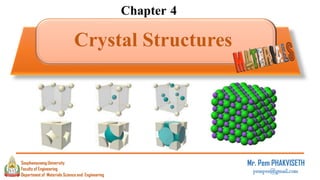
  • 21. 4.3 Crystal Structure Systems of Metals There are 3 common crystal structures of metals • Body Centered Cubic Structure (BCC) • Face Centered Cubic Structure (FCC) • Hexagonal Close Packed Structure (HCP) 21
  • 22. 1. Body Centered Cubic Structure (BCC) • Found in Chromium, Lithium, Iron and Tungsten etc. • have 1 atom in the middle And arranged in a straight line diagonally with the atoms in all 8 angles and connected throughout the crystal • The direction in which the atoms are packed the most is Diagonal line of the cube 22
  • 23. Determined a = lattice constant and R = atomic radius Will get a relationship Number of atoms 1 unit cell • All Angles 8 = (1/8) x 8 = 1 atom • Center point = 1 atom • Total 2 atom/unit cell 23
  • 25. 2. Face Centered Cubic Structure(FCC) • Found in copper, aluminum, silver and gold etc. • Will have atoms in all 8 corners and at the center point on all 6 sides • The direction in which the atoms are compressed most is the diagonal of each of the 6 sides of the cube. 25
  • 26. from unit cell atoms will touch each other diagonally of the side will Number of atom 1 unit cell • All angles 8 = (1/8) x 8 = 1 atom • All side 6 = (1/2) x 6 = 3 atom • Total 4 atom/unit cell 26 Diagonal side is equal to
  • 28. 28
  • 29. 3. Hexagonal-Close Packed (HCP) • Found in Magnesium, Titanium and Zinc etc. • The top and bottom planes have atoms close together to form a hexagon. And the central point of the plane The middle plane will have 3 atoms. • For ideal hcp , c/a = 1.633 1 Unit cell of HCP have 6 atom 29
  • 30. 1 Unit cell of HCP have 6 atom • Middle atom = 3 atom • Top-bottom atom = (1/2) x 2 = 1 atom • Atoms at the corner = (1/6) x 12 = 2 atom Cut times 1 remaining (1/2) Cut times 2 remaining (1/3) X (1/2) = (1/6) 30
  • 31. 31
  • 32. 4.3 Atomic Packing Factor (APF) • Is the value that tells the volume of the atom in unit cell • Assuming the shape of a circle of atoms so. 𝑨𝑷𝑭 = 𝑽𝒐𝒍𝒖𝒎𝒆 𝒐𝒇 𝒂𝒕𝒐𝒎 𝒊𝒏 𝒖𝒏𝒊𝒕 𝒄𝒆𝒍𝒍 𝒗𝒐𝒍𝒖𝒎𝒆 𝒐𝒇 𝒖𝒏𝒊𝒕 𝒄𝒆𝒍𝒍 • In BCC, APF = 0.68 • In FCC and HCP, APF=0.74 32
  • 33. Example of finding the Atomic Packing Factor for FCC Close – packed directions: Length = 4R = 2𝑎 Unit cell Contain: 6 × 1/2 + 8 × 1/8= 4 atom/ unit cell 33
  • 34. Example of finding the Atomic Packing Factor for FCC • The FCC structure in 1 cell has 4 atoms. • The volume of atoms is equal to (4/3) 𝜋𝑟3 • The volume of cell is equal to 𝑎3 34
  • 35. 4.4 Calculation to Density Computation of unit cell Theoretical density calculation Metal density (𝜌) can be calculated from take the mass of all the atoms, divided by the volume of 1 unit cell If the mass of atoms, A unit is atom mass unit (amu) to be divided by the Avogadro number (6.023 × 10²³ 𝑎𝑡𝑜𝑚𝑠/𝑚𝑜𝑙) In order to get the atomic mass 𝑀 𝑎𝑡𝑜𝑚 35
  • 36. 36
  • 37. 37
  • 38. Density of different types of materials Metals • Compact structure (Metallic bonding) • Very precious atomic mass Ceramics • Less compact structure(Covalent bonding) • Is usually a lighter element Polymers • Very compact structure(Usually an allotrope) • Is a very rare element (C,H,O) composites • Have medium properties 38
  • 40. 4.5 Crystallographic Directions • Is a vector indicating the direction in a crystal, used instead by [u,v,w] Which will be the full number (integer number) The smallest (Projection) of core x, y and z in unit cell. • Negative direction There will be a stroke above such as [ത100] Will be the opposite of [100] 40
  • 41. Point Coordinates • Determining the point in unit cell mainly like Cartesian coordinates • Except the value of x, y and z will show as a proportion of the length of unit vectors 41
  • 42. 42
  • 43. How to find the direction of the crystals in unit cell ( when knowing Coordinates) 1) Vector Used to indicate the direction must always pass through the origin 2) Set Coordinate Of the beginning (𝑥1, 𝑦1, 𝑧1) And the end of the direction (𝑥2, 𝑦2, 𝑧2) 3) Use Coordinate Destination minus Coordinate Origin : (𝑥2, 𝑦2, 𝑧2) − (𝑥1, 𝑦1, 𝑧1) = (𝑥2 − 𝑥1), (𝑦2 − 𝑦1), (𝑧2 − 𝑧1), 4) If there are fractions, the integer is the smallest value (Multiply LCM ) 5) To write the crystal direction index, write [uvw] No need to have any separator, If the value is negative, write it above the number, for example [ത100] 43
  • 44. Direction A 1) Starting point 0,0,0 Ending point 1,0,0 2) (1,0,0) - (0,0,0) = 1,0,0 3) Direction index = [100] Direction B 1) Starting point 0,0,0 Ending point 1,1,1 2) (1,1,1) - (0,0,0) = 1,1,1 3) Direction index = [111] Direction C 1) Starting point 1/2,1,0 Ending point 0,0,1 2) (0,0,1) - (1/2,1,0) = -1/2,-1,1 3) 2(-1/2,-1,1) = -1, -2, 2 4) Direction index = [ത1 ഥ2 2] 44
  • 45. Families and Symmetry In the direction of the crystal edge (cubic edge) [100],[010],[001],[ത100], [0ത10],[00ത1] =< 100 > Diagonal direction on both sides 6 (cubic face diagonals)=< 110 > Diagonal direction on both angle 4 (cubic face diagonals)=< 111 > 45
  • 46. • All direction vectors parallel to each other can use the same index because the starting point can be changed. • If the distance between atoms (atom spacing) in the direction parallel to the direction of the vector is the same We will consider that the vector direction is equal, for example In the direction of the crystal edge (cubic edge) [100],[010],[001],[ത100],[0ത10],[00ത1] =< 100 > Diagonal direction on both sides 6 (cubic face diagonals)=< 110 > Diagonal direction on both angle 4 (cubic face diagonals)=< 111 > • The symmetrical directions are called Family of crystallographic direction Must write in < > Only 46
  • 47. 4.6 Crystallographic planes • Means specifying the crystal plane that occurs in a unit cell, also known as Miller indices • Miller indices is' the reciprocals of the fractional intercepts which the plane makes with the crystallographic x, y and z axes of the three nonparallel edges of the cubic unit. cell ‘ • By writing the plane in the unit cell, the symbol (hkl) is used for the x, y and z axes respectively (when writing without commas, separated). 47
  • 48. Determining the crystal plane Or Miller index (Miller indices) (when knowing the intersection)) 1) Choose a plane that does not pass a point (000) 2) Find the point of intersection on all 3 axes of the plane and reverse the fractions of the point of intersection. 3) without any marks Separator and no space From picture beside The intersection of X, Y, Z axis is 1, ∞, ∞ Therefore, returning fractions to (reciprocals) 1, 0, 0 The miller indices is (100) 48
  • 50. From picture beside intercepts x, y, z is Τ1 2 , Τ1 2 , ∞ Reciprocals 2, 2, 0 Millers indices (220) From picture beside intercepts x, y, z is ∞, 1, 1 Reciprocal 0, 1, 1 Millers indices (011) 50
  • 53. 4.8 X-Ray Diffraction x-ray crystallography, also called x ray diffraction, is used to determine crystal structure by interpreting the diffraction patterns formed when x ray are scattered by the electron of atom in crystalline solids. x-rays are sent through a crystal to reveal the patterns in which the molecules and atom contained within the atom arranged. This x-ray crystallography was develop by physicist William Lawrence Bragg and his father William Henry Bragg in 1912 -1913, the younger Bragg develop Bragg's law, which connect the observed scattering with reflections from evenly spaced planes within the crystal. 53
  • 54. 𝜆: wavelength 𝑑: distance in unit cell 𝜃: angle between beam and surface in unit cell The equation is known as Bragg's law, also n is the order of reflection which may be integer (1,2,3....) consistent with not exceeding unity. Bragg's law 54
  • 55. The magnitude of the distance between two adjacent and parallel planes of atom (i.e.., interplanar spacing 𝑑ℎ𝑘𝑙 ). Is a function of the Miller indices (h, k and l )as well as the lattice parameter for example , for crystal structure that have cubic symmetry 𝑑ℎ𝑘𝑙 = 𝑎 ℎ2 + 𝑘2 + 𝑙2 In which a is the lattice parameter (unit cell edge length ). Relationships similar to equation above 55
  • 56. 56 Thank you for your attention !!! 감사합니다 !!! Department of Materials Science and Engineering Souphanouvong University Faculty of Engineering Next Chapter is Crystal Metals and Crystal Imperfections