SlideShare una empresa de Scribd logo
1 de 11
Praveen Vaidya, Department of Physics, SDMCET, Dharwad-02 UNIT - III
Page 1 of 11
SEMICONDUCTOR PHYSICS
The solids those are having short-range symmetry of atomic arrangement are either crystalline or
amorphous. These are mostly insulators.
The conductors and semiconductors have long range symmetry of atomic arrangement and they are
mostly in crystalline materials.
Valance and conduction band in semiconductors:
merger of 2N and 6N bands 2s and 2p into a single band with 8N available states. At effective
interatomic spacing (ao), the band with 8N energy states, splits into two bands with energy states 4N
each, separated by an energy gap or band gap Eg. Therefore, At zero K the Band Gap of a semiconductor
is defined as Energy difference between the maxima of valency band and minima of conduction band.
The upper band is conduction band, it is empty and the lower band called the valence band full with 4N
electrons.
For electric conduction, the electrons must transfer from valance band to conduction band; it is achieved
by the application of sufficient energy to electrons in valance band.
Band gap in insulators is high (Eg= 6 eV for carbon). Even at room temperature electrons cannot
sufficient energy to excite into conduction band.
For semiconductor bandgap is moderate; It is of the order of 1 eV.
For Ex., Germanium – 0.66eV Silicon – 1.12 eV
At 0K these materials are perfect insulators. But at higher temperature, energy available is sufficient to
for valence electrons to cross this energy gap, reach conduction band and show some conductivity.
In metals at 0k itself the electrons in conduction band or practically without external energy electron can
move to the conduction band hence show some conductivity.
Intrinsic and extrinsic semiconductors
The semiconductors are classified into Intrinsic and extrinsic semiconductors based on the presence of
impurities or dopants the basic distinctions are as follows.
The formation of bands in semiconductors will
follow the diamond (carbon) structure. Its
electronic configuration is . It is a given
in fig. 1. In the fig. taking interatomic distance on
X-axis and Energy on Y-axis when interatomic
distance reduces ( N atoms to form solid) energy
levels 1s, 2s, and 2p split into, 2N, 2N, and 6N
energy states and convert into bands. Further
reduction in the interatomic spacing results into
Fig. 1: The formation of energy bands is shown in above
plot due to variation in Energy of levels against lattice
constant (ao)
Praveen Vaidya, Department of Physics, SDMCET, Dharwad-02 UNIT - III
Page 2 of 11
DIFFERENCE BETWEEN INTRENSIC AND EXTRINSIC SEMICONDUCTORS:
Extrinsic semiconductor : To enhance the conductivity of semiconductor the concentration of charge
carriers are increased by adding some impurities.
Extrinsic semiconductors are formed when a small proportion of of impurity atoms (about 1 in 106)
are replaced by the atoms of pure (intrinsic) semiconductor crystals.
The process of adding impurity to pure semiconductor is called as doping. Impurity is called as dopant.
Extrinsic Semiconductors are classified into, 1) p-type and 2) n-type semiconductors resp.
Depending on the type of carrier doped the semiconductors classified into two types those are,
1. p-type semiconductor in which trivalent impurity element is doped and
2. n-type semiconductor in which pentavalent impurity element is doped
Position of Fermi energy in semiconductors: In case of semiconductors, the Fermi energy is defined
as; the average of highest energies possessed by the electrons in solid at a given temperature is also
called as Fermi energy, when related to semiconductors.
DIFFERENCE
INTRINSIC SEMICONDUCTOR p-type SEMICONDUCTOR
n-type Semiconductor
Presence of
impurity
The pure semiconducting
materials without the doping
of impurity.
Formed by doping Group
III element of periodic
table like Al, Ga, In.
Formed by doping Group V
element of periodic table,
impurity like P, As, Sb.
Density of
holes and
electrons
The number of free electrons
in the conduction band is
equal to the number of holes
in the valence band at T>0K
Holes are majority carriers
and electrons are minority
carriers.
Electrons are majority
carriers and Holes are
minority carriers.
Electrical
conductivity
Negligible conductivity as
direction of motion of equal
number of holes and
electrons in opposite
direction
Conductivity is due to
holes as they are majority
carriers.
Conductivity is high due to
electrons as they are
majority carriers.
Conductivit
y at 0k
Conductivity is zero and act
as perfect insulators
Small amount of
conductivity due to
presence of impurity.
Small amount of
conductivity due to presence
of impurity.
Position of
Fermi
energy
At the centre of Conduction
band minimum and valance
band maximum
At centre of accepter level
and valance band
maximum
At the centre of conduction
band minimum and donor
level.
Praveen Vaidya, Department of Physics, SDMCET, Dharwad-02 UNIT - III
Page 3 of 11
EC
EF
ED
EV
Conduction band
Valence band
n – type semiconductor
EC
EA
EF
EV
Conduction band
Valency band
p – type semiconductor
Fermi Energy in case of Intrinsic Semiconductors:
Therefore the the Fermi energy of the intrinsic semiconductor is given by
2
V
C
F
E
E
E

 and EC – EF = Eg/2
Where Eg is the energy gap of semiconductor.
Fermi energy in case of extrinsic semiconductors:
a) In case of p-type semiconductors:
An additional vacancy (hole) is generated by doping pure semiconductor with accepter type
impurity. This hole has energy slightly greater than valence band maximum. This additional hole finds
an energy level above the valance band. A new energy level is called as accepter level (EA). The energy
of the intrinsic holes in the valency band have heighest energy EV, therefore the Fermi energy in p-type
semiconductor is given by the average value of EA and EV.
2
A
V
F
E
E
E


b) In case of n-type semiconductors:
The impurity Electron generated by doping with doner type impurity is weakly bound to lattice. This
electron has slightly less energy than that of electron in the lowest state of conduction band. Hence, this
electron occupy in an energy level below the conduction band called as donor level (ED). Energy of the
intrinsic electron in the conduction band have lowest energy EC, therefore the Fermi energy in n-type
Eg
EC
EF
EV
Conduction band
Valency band
In case of intrinsic semiconductors, excited electrons possess
highest energy at least at the bottom of conduction band and
the electrons occupied vacant sites (holes) in valancy band
having highest energy at least at the top of valence band.
Hence to determine the Fermi energy one can consider the
average value of energy possessed by electrons at the bottom
of the conduction band (Ec) and energy possessed by
electrons at the top of the valence band (Ev),
Praveen Vaidya, Department of Physics, SDMCET, Dharwad-02 UNIT - III
Page 4 of 11
semiconductor is average value of ED and EV.
2
D
C
F
E
E
E


Classification of semiconductor on the basis of the Band gap
The semiconductors are classified into two types on the basis of the bandgap.
1. Indirect Bandgap semiconductors
2. Direct Bandgap semiconductors
1. Indirect Bandgap Semiconductors:
The semiconductor materials in which the maximum of valance band is not exactly below the minimum
conduction band are called Indirect band gap semiconductors. It is shown in the E-k diagram (Fig. 2b).
to valance band it given out phonon and reaches valance band maxima radiating heat or gives non-
irradiative transition Therefore, indirect bandgap semiconductors are not suitable only for electrical
properties. As biasing circuit of diodes, as rectifiers and switches etc.
Examples of Indirect bandgap semiconductors are Silicon, Germanium. Tellurium GaP, SiC etc.
2. Direct Bandgap Semiconductors:
The semiconductors in which maximum of valance band is exactly below the minimum conduction band
to conserve energy and momentum are called as Direct bandgap semiconductors. (E-k diagram Fig.2a).
When transition takes place from valance band to conduction band, by absorbing the photon, the energy
as well as momentum are conserved, because the maxima of valance band and minima conduction band
are in same ‘k’ value, similarly when transition takes place from conduction band to valance band
electron give out the photon (electromagnetic radiation) of energy equivalent to that it absorbed without
giving intermediate particle.
Material Direct / Indirect Bandgap Band Gap Energy at 300 K (eV)
Elements C (diamond)
Ge
Si
Indirect
Indirect
Indirect
5.47
0.66
1.12
When transition takes place from valance band to conduction
band by absorbing the photon, the energy is conserved but not
momentum, because the maximum of valance band and
minimum conduction band are not in same ‘k’ value, this is
compensated by the quantum particle called phonon, therefore
there is interaction of electron, photon and phonon.
Similarly, when transition takes place from conduction band
Fig 2a Fig 2b
Praveen Vaidya, Department of Physics, SDMCET, Dharwad-02 UNIT - III
Page 5 of 11
Groups III-V
compounds
GaAs
InAs
GaP
GaN
Direct
Direct
Indirect
Direct
1.42
0.36
2.26
3.36
Groups II-VI
compounds
ZnO
CdSe
ZnS
Direct
Direct
Direct
3.35
1.70
3.68
Examples of Direct band gap semiconductors are Compound semiconductors (The semiconductors
formed by compsite of two or more elements) Like, Gallium Arsenide (GaAs), Cadmium Telluride
(CdTe), Zinc Sulphide (ZnS), etc.,
The compound semiconductor are divided into III-V and II-VI semiconductor, in farmer the Group III
and Group V elements are composed ( Ga and As – GaAs) and in later Group II and Group VI (Cd and
Te – CdTe) elements of the periodic table composed to become semiconductor respectively.
This combination is made because to get the semiconductors required bandgap and the higher bandgap
semiconductors.
The higher Direct bandgap semiconductors are emit the electromagnetic radiation in Near IR, Visible and
in Ultra violet region.
These semiconductors are highly useful in optoelectronic properties like in case producing Light emitting
diods (LEDs), LASERs, Sensors and Solar Photovoltaic’s etc.,
GaAs is the semiconductor maximum used in satellite and space shuttle solar panel.
Distinction between Direct Bandgap and Indirct bandgap Seemiconductors
Sl. No. Direct Band gap semiconductor Indirect Band gap semiconductor
1 A direct band-gap (DBG) semiconductor is
one in which the maximum energy level of
the valence band aligns with the minimum
energy level of the conduction band with
respect to momentum.
A indirect band-gap (IDBG) semiconductor is
one in which the maximum energy level of the
valence band are misaligned with the minimum
energy level of the conduction band with respect
to momentum.
2 In a DBG semiconductor, a direct
recombination takes place with the release
of the energy equal to the energy difference
between the recombining particles
Due to a relative difference in the momentum,
first, the momentum is conserved by release of
energy and only after both the momenta align
themselves, a recombination occurs
accompanied with the release of energy
3. The efficiency factor of a DBG
semiconductor is much more than that of an
IBG semiconductor
The probability of a radiative recombination, is
much less in comparison to that in case of DBG
semiconductors
4 The most thoroughly investigated and
studied DBG semiconductor material is
Gallium Arsenide (GaAs).
The two well-known intrinsic semiconductors,
Silicon and Germanium are both IBG
semiconductors
Praveen Vaidya, Department of Physics, SDMCET, Dharwad-02 UNIT - III
Page 6 of 11
5 DBG semiconductors are always preferred
over IBG for making optical sources
The IBG semiconductors cannot be used to
manufacture optical sources.
Carrier concentration in semiconductors
It is known that electrons and holes are the current carriers in semiconductors.
In case of intrinsic semiconductors, at temperature above 0 k, the electrons and holes are created as a pair
due to breaking of bonds. This phenomenon is called electron hole pair generation.
If ‘n’ is number of electrons per unit volume (electron density) in conduction band and ‘p’ is number
holes per unit volume (hole density) in valance band, then
n = p = ni
The conductivity of semiconductor is go on increases as temperature increases, so one can find large
number of electrons in conduction band and that of holes in valance band.
The density of carriers can be found by using the theory of Fermi-dirac statistics, according
which,
Density of electrons in conduction band between the energy E (highest energy level occupied by
electron) and EC (lowest energy of electron near conduction band) is given by,
Where gc(E) is the density of states in the conduction
band and f(E) is the Fermi function.
Substituting the value of gc(E), f(E) and integrating we get,
The electron concentration (no) is (taking E = ∞, represents the top of conduction band)
---(1)
dE
e
E
E
m
h
kT
E
E
E
c
e
F
C





 



 

2
/
3
3
2
8
dE
e
E
E
e
m
h
kT
E
E
E
c
kT
E
E
e
C
C
C
F





 







 

 

2
/
3
3
2
8 2
/
3
2
/
3
3
)
(
2
2
8
kT
e
m
h
kT
E
E
e
C
F

 




 







 










 kT
E
E
e
F
C
e
h
kT
m
2
/
3
2
2
2

This can be written as





 

 kT
E
E
C
F
C
e
N - Electron carrier concentration.
Praveen Vaidya, Department of Physics, SDMCET, Dharwad-02 UNIT - III
Page 7 of 11
Where NC is given by,
Similarly, density of holes in valance band is given by Fermi dirac distribution,
Substituting the value of gc(E), f(E) and integrating we get,
dE
e
E
E
m
h
p kT
E
E
EV
V
h
o F









 



 1
1
1
2
8 2
/
3
3

dE
e
E
E
e
m
h
kT
E
E
E
V
kT
E
E
h
F
V
V
F





 








 


 

2
/
3
3
2
8 2
/
3
2
/
3
3
)
(
2
2
8
kT
e
m
h
kT
E
E
h
V
F

 




 








 










 kT
E
E
h
V
F
e
h
kT
m
2
/
3
2
2
2

This can be written as





 

 kT
E
E
V
V
F
e
N - Hole carrier concentration
Where
In above equations of electron and hole concentration of a intrinsic semiconductors Where Nc and Nv are
the temperature-dependent material constant known as the effective density of states in conduction
band and valance band respectively.
In the above two integrals, the actual location of the top of the conduction band/bottom of valance does
not need to be known as the Fermi function goes to zero at higher energies in conduction band/lower
inergies in valance band.
Intrinsic carrier density: We know that, in intrinsic semiconductor,
n = p = ni
therefore, nopo = ni
2














 

kT
E
E
C
i
C
F
e
N
n
2







 




 

kT
E
E
V
V
F
e
N =





 

kT
E
E
V
C
V
C
e
N
N ,
Praveen Vaidya, Department of Physics, SDMCET, Dharwad-02 UNIT - III
Page 8 of 11
but EC – EV = Eg










kT
E
V
C
i
g
e
N
N
n
2
2
/
1
)
(
Substituting the values of NC and NV ,
2
/
3
4
/
3
2
/
3
2
)
(
2
2 T
m
m
h
k
n h
e
i









 








kT
Eg
e
2
The above equation gives the net carrier concentration in an intrinsic semiconductor.
Where Nc(300 K) is the effective density of states at 300 K
Mobility of charge carriers:
At room temperature electrons semiconductor; excite to conduction band, leaving behind holes. Under
the application electric field E, electrons and holes accelerate in opposite direction, hence drift velocity,
‘ q’ must be taken as n – for electrons and p – for holes.
The ratio of the drift velocity to the applied electric field is known as mobility is given by
For electrons in conduction band
Electric Conductivity of Intrinsic Semiconductors:
As per free electron theory, the conductivity σ of a metal is given by the expression,
m
ne 

2
 , but
m
e
e

 
Therefore, σ = neμe
Where n is the number of free electrons per unit volume of the conductor i.e. electron density, e is the
electron charge and μe is the electron mobility.
Conductivity due to electron in semiconducto is neμe
Similarly, conductivity due to holes is peμh
Since, in semiconductors the conduction is due to free electrons as well as holes.
Electric conductivity of semiconductor is
σ = σn + σp = neμe + peμh
Praveen Vaidya, Department of Physics, SDMCET, Dharwad-02 UNIT - III
Page 9 of 11
= e(nμe + pμh )
Since in intrinsic semiconductors n = p = ni, the intrinsic concentration of holes or free electron in the
semiconductor.
Therefore above equation takes the form,
σ = nieμe + ni eμh
So conductivity in intrinsic semiconductor.
σ = nie (μe + μh )
HALL EFFECT:
When a transverse magnetic field is applied to the conductor carrying current a voltage develop in the
direction perpendicular to both direction of current and magnetic field respectively, is called as Hall
Effect and voltage is called a Hall voltage.
This phenomenon was discovered by E.H. Hall in 1879.
Consider a specimen of conductor in the form thin strip with width (w) and thickness (d) and length (l).
On application of electric field along length a current ‘I’ set up through the conductor. If the a magnetic
field (B) applied in the direction thickness (d), then a potential difference (VH) developed in the direction
of width (w) is measured with a millivoltmeter.
In following figure, a conventional current flow along +ve X –axis (hence electron motion is along –ve
X-axis) by the application electric field Ex and built current density Jx, on application Magnetic field
along Z-axis (Bz), the electron experience transverse force called Lorentz force, is given by,
F = – e (vx Bz)
due to this force accumulation of charges at the ends of conductor, which builds electric field (Ey). along
Y-axis, this electric force along Y-axis is given by,
Fy = – e Ey
Under equilibrium, these two forces balance each other is given by,
Ey = vx Bz ═> vx = Ey/Bz
Praveen Vaidya, Department of Physics, SDMCET, Dharwad-02 UNIT - III
Page 10 of 11
The current density along X-direction is given by,
Jx = – nevx ═> Jx = neEy /Bz
H
x
y
R
z
B
J
E
ne



1
RH here is called as Hall coefficient.
But, Ey = VH/w (w – width of the conductor)
Therefore,
J = – neVy/wBz or,
ne
z
JwB
ne
z
JwB
H
V 



J = I/A = I/dxw,
Therefore,
dne
z
IB
H
V 

VH is called as hall voltage.
Where d and w are thickness and width of the sample perpendicular to direction of current.
Importance of Hall Effect Measurements:
# Invaluable for characterizing semiconductor materials, whether they are silicon-based, compound
semiconductors, thin-film materials for solar cells, or nanoscale materials like graphene.
#The measurements span low-resistance (highly doped semiconductors, high-temp. superconductors and
GMR/ TMR materials and high-resistance semiconductors including semi-insulating GaAs, GAN etc.
# Useful for determining various material parameters, but the primary one is the Hall voltage (VH).
Carrier mobility, carrier concentration (n), Hall coefficient (RH) and the carrier types.
As researchers develop next-generation ICs and more efficient semiconductor materials, they’re
particularly interested in materials with high carrier mobility, which is what’s sparked much of the
interest in graphene. This one atom-thick form of carbon exhibits the quantum Hall Effect and, as a
result, relativistic electron current flow. Researchers consider Hall Effect measurements crucial to the
future of the electronics industry.
Praveen Vaidya, Department of Physics, SDMCET, Dharwad-02 UNIT - III
Page 11 of 11
]
Fermi dirac statistics applied to semiconductors (Not for syllabus)
The density of states in a semiconductor was obtained by
solving the Schrödinger equation for the particles in the
semiconductor. Rather than using the actual and very complex
potential in the semiconductor, we use the simple particle-in-a
box model, where one assumes that the particle is free to move
within the material.
For an electron which behaves as a free particle with effective
mass, m*
, the density of states was derived using,
where Ec is the bottom of the conduction band below
which the density of states is zero. The density of states
for holes in the valence band is given by:
The densityof electrons in a semiconductor is related to the
densityof available statesand the probabilitythat each of these
states is occupied.
Questions:
1. Distinguish p-type and n-type
semiconductors.
2. How the energy gap of semiconductor is
different from its Fermi energy?
3. With a band diagram elucidate the position
Fermi energy in intrinsic and extrinsic
semiconductors.
4. What you mean by doping? Distinguish
the semiconductors based on nature of
dopant with diagram showing the band gap
(Distinguish the intrinsic and extrinsic
semiconductors) and Fermi level.
5 What are carriers related to semiconductors.
Starting from the expression for the density
of state and Fermi direct distribution, arrive
at the expression for the effective density of
states
6 Derive expressions for the intrinsic carrier
concentration (ni) of semiconductor and
show that ni independent of Fermi energy.
7 Derive an expression for the electric
conductivity of a semiconductor in terms of
carrier concentration and mobility.
8 Write any three applications of hall effect
9 Derive an expression for hall voltage and
hall coefficient of a given conductor.
The densityof occupied states per unit volume and energy, n(E), ), is
simply the product of the density of states in the conduction band,
gc(E) and the Fermi-Dirac probability function, f(E), (also called the
Fermi function):
Since holes correspond to empty states in the valence band, the
probability of having a hole equals the probability that a particular
state is not filled, so that the hole density per unit energy, p(E),
equals:
Where gv(E) is the densityof states in the valence band. The density
of carriersis then obtained by integrating the density of carriers per
unit energy over all possible energies within a band. A general
expression is derived as well as an approximate analytic solution,
which is valid for non-degenerate semiconductors. In addition, we
also present the Joyce-Dixon approximation, an approximate solution
useful when describing degenerate semiconductors.

Más contenido relacionado

La actualidad más candente

Unit 1 Mechanism of Conduction in Semiconductors
Unit 1 Mechanism of Conduction in SemiconductorsUnit 1 Mechanism of Conduction in Semiconductors
Unit 1 Mechanism of Conduction in SemiconductorsDr Piyush Charan
 
B.tech sem i engineering physics u ii chapter 1-band theory of solid
B.tech sem i engineering physics u ii chapter 1-band theory of solidB.tech sem i engineering physics u ii chapter 1-band theory of solid
B.tech sem i engineering physics u ii chapter 1-band theory of solidRai University
 
SEMICONDUCTOR PHYSICS.ppt
SEMICONDUCTOR  PHYSICS.pptSEMICONDUCTOR  PHYSICS.ppt
SEMICONDUCTOR PHYSICS.pptVijayAECE1
 
QUANTITIVE EXPRESSION FOR DEBYE SCREENING AND QUASINEUTRAL PLASMA
QUANTITIVE EXPRESSION FOR DEBYE SCREENING AND QUASINEUTRAL PLASMAQUANTITIVE EXPRESSION FOR DEBYE SCREENING AND QUASINEUTRAL PLASMA
QUANTITIVE EXPRESSION FOR DEBYE SCREENING AND QUASINEUTRAL PLASMAAnitaMalviya
 
Direct and in direct band gap-Modern Physics
Direct and in direct band gap-Modern PhysicsDirect and in direct band gap-Modern Physics
Direct and in direct band gap-Modern PhysicsChandra Prakash Pandey
 
Band theory of solid
Band theory of solidBand theory of solid
Band theory of solidKeyur Patel
 
Energy band and energy gap by Pratimesh pathak
Energy band and energy gap by Pratimesh pathakEnergy band and energy gap by Pratimesh pathak
Energy band and energy gap by Pratimesh pathakPratimesh Pathak
 
semiconductor - description and application
semiconductor - description and applicationsemiconductor - description and application
semiconductor - description and applicationBishnupadaSarkar2
 
L-1.4-Energy bands in solids.pptx
L-1.4-Energy bands in solids.pptxL-1.4-Energy bands in solids.pptx
L-1.4-Energy bands in solids.pptxVaibhavSingh222360
 
Introduction to superconductivity
Introduction to superconductivityIntroduction to superconductivity
Introduction to superconductivitysenkur
 
Chapter3 introduction to the quantum theory of solids
Chapter3 introduction to the quantum theory of solidsChapter3 introduction to the quantum theory of solids
Chapter3 introduction to the quantum theory of solidsK. M.
 
Band theory of solids
Band theory of solidsBand theory of solids
Band theory of solidsutpal sarkar
 

La actualidad más candente (20)

Semiconductors
SemiconductorsSemiconductors
Semiconductors
 
Unit 1 Mechanism of Conduction in Semiconductors
Unit 1 Mechanism of Conduction in SemiconductorsUnit 1 Mechanism of Conduction in Semiconductors
Unit 1 Mechanism of Conduction in Semiconductors
 
B.tech sem i engineering physics u ii chapter 1-band theory of solid
B.tech sem i engineering physics u ii chapter 1-band theory of solidB.tech sem i engineering physics u ii chapter 1-band theory of solid
B.tech sem i engineering physics u ii chapter 1-band theory of solid
 
SEMICONDUCTOR PHYSICS.ppt
SEMICONDUCTOR  PHYSICS.pptSEMICONDUCTOR  PHYSICS.ppt
SEMICONDUCTOR PHYSICS.ppt
 
Density of states of bulk semiconductor
Density of states of bulk semiconductorDensity of states of bulk semiconductor
Density of states of bulk semiconductor
 
QUANTITIVE EXPRESSION FOR DEBYE SCREENING AND QUASINEUTRAL PLASMA
QUANTITIVE EXPRESSION FOR DEBYE SCREENING AND QUASINEUTRAL PLASMAQUANTITIVE EXPRESSION FOR DEBYE SCREENING AND QUASINEUTRAL PLASMA
QUANTITIVE EXPRESSION FOR DEBYE SCREENING AND QUASINEUTRAL PLASMA
 
Band theory
Band theoryBand theory
Band theory
 
SOMMERFELD MODEL Maya yadav ppt
SOMMERFELD MODEL Maya yadav pptSOMMERFELD MODEL Maya yadav ppt
SOMMERFELD MODEL Maya yadav ppt
 
Band theory
Band theoryBand theory
Band theory
 
Solid state electronics
Solid state electronicsSolid state electronics
Solid state electronics
 
Direct and in direct band gap-Modern Physics
Direct and in direct band gap-Modern PhysicsDirect and in direct band gap-Modern Physics
Direct and in direct band gap-Modern Physics
 
Superconductivity
SuperconductivitySuperconductivity
Superconductivity
 
Band theory of solid
Band theory of solidBand theory of solid
Band theory of solid
 
Energy band and energy gap by Pratimesh pathak
Energy band and energy gap by Pratimesh pathakEnergy band and energy gap by Pratimesh pathak
Energy band and energy gap by Pratimesh pathak
 
semiconductor - description and application
semiconductor - description and applicationsemiconductor - description and application
semiconductor - description and application
 
L-1.4-Energy bands in solids.pptx
L-1.4-Energy bands in solids.pptxL-1.4-Energy bands in solids.pptx
L-1.4-Energy bands in solids.pptx
 
Semiconductors
SemiconductorsSemiconductors
Semiconductors
 
Introduction to superconductivity
Introduction to superconductivityIntroduction to superconductivity
Introduction to superconductivity
 
Chapter3 introduction to the quantum theory of solids
Chapter3 introduction to the quantum theory of solidsChapter3 introduction to the quantum theory of solids
Chapter3 introduction to the quantum theory of solids
 
Band theory of solids
Band theory of solidsBand theory of solids
Band theory of solids
 

Similar a Semiconductor physics for undergraduates

15 lekshmi subject slide.pptx
15 lekshmi subject slide.pptx15 lekshmi subject slide.pptx
15 lekshmi subject slide.pptxjishakurian99
 
Class 12 th semiconductor part 1
Class 12 th semiconductor part 1Class 12 th semiconductor part 1
Class 12 th semiconductor part 1Priyanka Jakhar
 
Class 12 th semiconductor part 1
Class 12 th semiconductor part 1Class 12 th semiconductor part 1
Class 12 th semiconductor part 1Priyanka Jakhar
 
Diploma sem 2 applied science physics-unit 3-chap-1 band theory of solid
Diploma sem 2 applied science physics-unit 3-chap-1 band theory of solidDiploma sem 2 applied science physics-unit 3-chap-1 band theory of solid
Diploma sem 2 applied science physics-unit 3-chap-1 band theory of solidRai University
 
Semiconcuctor devices introduction
Semiconcuctor devices  introductionSemiconcuctor devices  introduction
Semiconcuctor devices introductionRachnaRishi2
 
Electronic Devices and Circuits by Dr. R.Prakash Rao
Electronic Devices and Circuits by Dr. R.Prakash RaoElectronic Devices and Circuits by Dr. R.Prakash Rao
Electronic Devices and Circuits by Dr. R.Prakash Raorachurivlsi
 
Lasers & semiconductors 2008 prelim solutions
Lasers & semiconductors 2008 prelim solutionsLasers & semiconductors 2008 prelim solutions
Lasers & semiconductors 2008 prelim solutionsJohn Jon
 
solids_and_semiconductor_devices_1.ppt
solids_and_semiconductor_devices_1.pptsolids_and_semiconductor_devices_1.ppt
solids_and_semiconductor_devices_1.pptmragarwal
 
Theoretically investigate the nature of direct band gap of novel materials
Theoretically investigate the nature of direct band gap of novel materialsTheoretically investigate the nature of direct band gap of novel materials
Theoretically investigate the nature of direct band gap of novel materialsUCP
 
B.Tech sem I Engineering Physics U-II Chapter 1-Band theory of solid
B.Tech sem I Engineering Physics U-II Chapter 1-Band theory of solidB.Tech sem I Engineering Physics U-II Chapter 1-Band theory of solid
B.Tech sem I Engineering Physics U-II Chapter 1-Band theory of solidAbhi Hirpara
 
The semiconductors.docx
The semiconductors.docxThe semiconductors.docx
The semiconductors.docxmadiana01
 
Applied physics unit4- part1
Applied physics unit4- part1Applied physics unit4- part1
Applied physics unit4- part1UmayalSundariAR
 
Coulomb Blockade Oscillations
Coulomb Blockade OscillationsCoulomb Blockade Oscillations
Coulomb Blockade OscillationsDeepak Rajput
 
Semiconductors
SemiconductorsSemiconductors
SemiconductorsA B Shinde
 
Electrical Measurements for Semiconducting Devices
Electrical Measurements for Semiconducting DevicesElectrical Measurements for Semiconducting Devices
Electrical Measurements for Semiconducting DevicesYogesh Patil
 

Similar a Semiconductor physics for undergraduates (20)

Energy bands and gaps in semiconductor
Energy bands and gaps in semiconductorEnergy bands and gaps in semiconductor
Energy bands and gaps in semiconductor
 
15 lekshmi subject slide.pptx
15 lekshmi subject slide.pptx15 lekshmi subject slide.pptx
15 lekshmi subject slide.pptx
 
Class 12 th semiconductor part 1
Class 12 th semiconductor part 1Class 12 th semiconductor part 1
Class 12 th semiconductor part 1
 
Class 12 th semiconductor part 1
Class 12 th semiconductor part 1Class 12 th semiconductor part 1
Class 12 th semiconductor part 1
 
PPT.ppt
PPT.pptPPT.ppt
PPT.ppt
 
Diploma sem 2 applied science physics-unit 3-chap-1 band theory of solid
Diploma sem 2 applied science physics-unit 3-chap-1 band theory of solidDiploma sem 2 applied science physics-unit 3-chap-1 band theory of solid
Diploma sem 2 applied science physics-unit 3-chap-1 band theory of solid
 
Semiconcuctor devices introduction
Semiconcuctor devices  introductionSemiconcuctor devices  introduction
Semiconcuctor devices introduction
 
Electronic Devices and Circuits by Dr. R.Prakash Rao
Electronic Devices and Circuits by Dr. R.Prakash RaoElectronic Devices and Circuits by Dr. R.Prakash Rao
Electronic Devices and Circuits by Dr. R.Prakash Rao
 
Lasers & semiconductors 2008 prelim solutions
Lasers & semiconductors 2008 prelim solutionsLasers & semiconductors 2008 prelim solutions
Lasers & semiconductors 2008 prelim solutions
 
Basic electronics
Basic electronicsBasic electronics
Basic electronics
 
solids_and_semiconductor_devices_1.ppt
solids_and_semiconductor_devices_1.pptsolids_and_semiconductor_devices_1.ppt
solids_and_semiconductor_devices_1.ppt
 
Theoretically investigate the nature of direct band gap of novel materials
Theoretically investigate the nature of direct band gap of novel materialsTheoretically investigate the nature of direct band gap of novel materials
Theoretically investigate the nature of direct band gap of novel materials
 
B.Tech sem I Engineering Physics U-II Chapter 1-Band theory of solid
B.Tech sem I Engineering Physics U-II Chapter 1-Band theory of solidB.Tech sem I Engineering Physics U-II Chapter 1-Band theory of solid
B.Tech sem I Engineering Physics U-II Chapter 1-Band theory of solid
 
The semiconductors.docx
The semiconductors.docxThe semiconductors.docx
The semiconductors.docx
 
Bandtheory of solids
Bandtheory of solidsBandtheory of solids
Bandtheory of solids
 
Applied physics unit4- part1
Applied physics unit4- part1Applied physics unit4- part1
Applied physics unit4- part1
 
Coulomb Blockade Oscillations
Coulomb Blockade OscillationsCoulomb Blockade Oscillations
Coulomb Blockade Oscillations
 
Semiconductors
SemiconductorsSemiconductors
Semiconductors
 
Electrical Measurements for Semiconducting Devices
Electrical Measurements for Semiconducting DevicesElectrical Measurements for Semiconducting Devices
Electrical Measurements for Semiconducting Devices
 
AE DIGITAL NOTES.pdf
AE DIGITAL NOTES.pdfAE DIGITAL NOTES.pdf
AE DIGITAL NOTES.pdf
 

Más de Praveen Vaidya

Fundamentals of Superconductivity and its applications
Fundamentals of Superconductivity and its applicationsFundamentals of Superconductivity and its applications
Fundamentals of Superconductivity and its applicationsPraveen Vaidya
 
torsinal pendulum.docx
torsinal pendulum.docxtorsinal pendulum.docx
torsinal pendulum.docxPraveen Vaidya
 
Optical fiber Experiment.docx
Optical fiber Experiment.docxOptical fiber Experiment.docx
Optical fiber Experiment.docxPraveen Vaidya
 
To detemine the wavelength of semiconductor laser
To detemine the wavelength of semiconductor laserTo detemine the wavelength of semiconductor laser
To detemine the wavelength of semiconductor laserPraveen Vaidya
 
Fundamentals of modern physics, the de-Broglie hypothesis
Fundamentals of modern physics, the de-Broglie hypothesisFundamentals of modern physics, the de-Broglie hypothesis
Fundamentals of modern physics, the de-Broglie hypothesisPraveen Vaidya
 
Young's modulus by single cantilever method
Young's modulus by single cantilever methodYoung's modulus by single cantilever method
Young's modulus by single cantilever methodPraveen Vaidya
 
Fundamenals of magnetism and applications
Fundamenals of magnetism and applicationsFundamenals of magnetism and applications
Fundamenals of magnetism and applicationsPraveen Vaidya
 
Introduction nanoscience
Introduction nanoscienceIntroduction nanoscience
Introduction nanosciencePraveen Vaidya
 
Zener diode experiment.
Zener diode experiment.Zener diode experiment.
Zener diode experiment.Praveen Vaidya
 
Maxwell's equations and their derivations.
Maxwell's equations and their derivations.Maxwell's equations and their derivations.
Maxwell's equations and their derivations.Praveen Vaidya
 
Series parallel resonance circuit
Series parallel resonance circuitSeries parallel resonance circuit
Series parallel resonance circuitPraveen Vaidya
 
Quantum mechanics for Engineering Students
Quantum mechanics for Engineering StudentsQuantum mechanics for Engineering Students
Quantum mechanics for Engineering StudentsPraveen Vaidya
 
Introduction to Elasticity of materials
Introduction to Elasticity of materialsIntroduction to Elasticity of materials
Introduction to Elasticity of materialsPraveen Vaidya
 
Optical fibers Theory and applications
Optical fibers Theory and applicationsOptical fibers Theory and applications
Optical fibers Theory and applicationsPraveen Vaidya
 
Fundamentals of modern physics
Fundamentals of modern physicsFundamentals of modern physics
Fundamentals of modern physicsPraveen Vaidya
 
fundamentals of optical fiber
fundamentals of optical fiberfundamentals of optical fiber
fundamentals of optical fiberPraveen Vaidya
 
degradation of pollution and photocatalysis
degradation of pollution and photocatalysisdegradation of pollution and photocatalysis
degradation of pollution and photocatalysisPraveen Vaidya
 
Energy bands and electrical properties of metals new
Energy bands and electrical properties of metals newEnergy bands and electrical properties of metals new
Energy bands and electrical properties of metals newPraveen Vaidya
 

Más de Praveen Vaidya (20)

Fundamentals of Superconductivity and its applications
Fundamentals of Superconductivity and its applicationsFundamentals of Superconductivity and its applications
Fundamentals of Superconductivity and its applications
 
torsinal pendulum.docx
torsinal pendulum.docxtorsinal pendulum.docx
torsinal pendulum.docx
 
relativity.pdf
relativity.pdfrelativity.pdf
relativity.pdf
 
Optical fiber Experiment.docx
Optical fiber Experiment.docxOptical fiber Experiment.docx
Optical fiber Experiment.docx
 
spring constant.docx
spring constant.docxspring constant.docx
spring constant.docx
 
To detemine the wavelength of semiconductor laser
To detemine the wavelength of semiconductor laserTo detemine the wavelength of semiconductor laser
To detemine the wavelength of semiconductor laser
 
Fundamentals of modern physics, the de-Broglie hypothesis
Fundamentals of modern physics, the de-Broglie hypothesisFundamentals of modern physics, the de-Broglie hypothesis
Fundamentals of modern physics, the de-Broglie hypothesis
 
Young's modulus by single cantilever method
Young's modulus by single cantilever methodYoung's modulus by single cantilever method
Young's modulus by single cantilever method
 
Fundamenals of magnetism and applications
Fundamenals of magnetism and applicationsFundamenals of magnetism and applications
Fundamenals of magnetism and applications
 
Introduction nanoscience
Introduction nanoscienceIntroduction nanoscience
Introduction nanoscience
 
Zener diode experiment.
Zener diode experiment.Zener diode experiment.
Zener diode experiment.
 
Maxwell's equations and their derivations.
Maxwell's equations and their derivations.Maxwell's equations and their derivations.
Maxwell's equations and their derivations.
 
Series parallel resonance circuit
Series parallel resonance circuitSeries parallel resonance circuit
Series parallel resonance circuit
 
Quantum mechanics for Engineering Students
Quantum mechanics for Engineering StudentsQuantum mechanics for Engineering Students
Quantum mechanics for Engineering Students
 
Introduction to Elasticity of materials
Introduction to Elasticity of materialsIntroduction to Elasticity of materials
Introduction to Elasticity of materials
 
Optical fibers Theory and applications
Optical fibers Theory and applicationsOptical fibers Theory and applications
Optical fibers Theory and applications
 
Fundamentals of modern physics
Fundamentals of modern physicsFundamentals of modern physics
Fundamentals of modern physics
 
fundamentals of optical fiber
fundamentals of optical fiberfundamentals of optical fiber
fundamentals of optical fiber
 
degradation of pollution and photocatalysis
degradation of pollution and photocatalysisdegradation of pollution and photocatalysis
degradation of pollution and photocatalysis
 
Energy bands and electrical properties of metals new
Energy bands and electrical properties of metals newEnergy bands and electrical properties of metals new
Energy bands and electrical properties of metals new
 

Último

Unit 3 Emotional Intelligence and Spiritual Intelligence.pdf
Unit 3 Emotional Intelligence and Spiritual Intelligence.pdfUnit 3 Emotional Intelligence and Spiritual Intelligence.pdf
Unit 3 Emotional Intelligence and Spiritual Intelligence.pdfDr Vijay Vishwakarma
 
Micro-Scholarship, What it is, How can it help me.pdf
Micro-Scholarship, What it is, How can it help me.pdfMicro-Scholarship, What it is, How can it help me.pdf
Micro-Scholarship, What it is, How can it help me.pdfPoh-Sun Goh
 
Jamworks pilot and AI at Jisc (20/03/2024)
Jamworks pilot and AI at Jisc (20/03/2024)Jamworks pilot and AI at Jisc (20/03/2024)
Jamworks pilot and AI at Jisc (20/03/2024)Jisc
 
HMCS Max Bernays Pre-Deployment Brief (May 2024).pptx
HMCS Max Bernays Pre-Deployment Brief (May 2024).pptxHMCS Max Bernays Pre-Deployment Brief (May 2024).pptx
HMCS Max Bernays Pre-Deployment Brief (May 2024).pptxEsquimalt MFRC
 
Jual Obat Aborsi Hongkong ( Asli No.1 ) 085657271886 Obat Penggugur Kandungan...
Jual Obat Aborsi Hongkong ( Asli No.1 ) 085657271886 Obat Penggugur Kandungan...Jual Obat Aborsi Hongkong ( Asli No.1 ) 085657271886 Obat Penggugur Kandungan...
Jual Obat Aborsi Hongkong ( Asli No.1 ) 085657271886 Obat Penggugur Kandungan...ZurliaSoop
 
Sociology 101 Demonstration of Learning Exhibit
Sociology 101 Demonstration of Learning ExhibitSociology 101 Demonstration of Learning Exhibit
Sociology 101 Demonstration of Learning Exhibitjbellavia9
 
Wellbeing inclusion and digital dystopias.pptx
Wellbeing inclusion and digital dystopias.pptxWellbeing inclusion and digital dystopias.pptx
Wellbeing inclusion and digital dystopias.pptxJisc
 
REMIFENTANIL: An Ultra short acting opioid.pptx
REMIFENTANIL: An Ultra short acting opioid.pptxREMIFENTANIL: An Ultra short acting opioid.pptx
REMIFENTANIL: An Ultra short acting opioid.pptxDr. Ravikiran H M Gowda
 
NO1 Top Black Magic Specialist In Lahore Black magic In Pakistan Kala Ilam Ex...
NO1 Top Black Magic Specialist In Lahore Black magic In Pakistan Kala Ilam Ex...NO1 Top Black Magic Specialist In Lahore Black magic In Pakistan Kala Ilam Ex...
NO1 Top Black Magic Specialist In Lahore Black magic In Pakistan Kala Ilam Ex...Amil baba
 
Plant propagation: Sexual and Asexual propapagation.pptx
Plant propagation: Sexual and Asexual propapagation.pptxPlant propagation: Sexual and Asexual propapagation.pptx
Plant propagation: Sexual and Asexual propapagation.pptxUmeshTimilsina1
 
HMCS Vancouver Pre-Deployment Brief - May 2024 (Web Version).pptx
HMCS Vancouver Pre-Deployment Brief - May 2024 (Web Version).pptxHMCS Vancouver Pre-Deployment Brief - May 2024 (Web Version).pptx
HMCS Vancouver Pre-Deployment Brief - May 2024 (Web Version).pptxmarlenawright1
 
This PowerPoint helps students to consider the concept of infinity.
This PowerPoint helps students to consider the concept of infinity.This PowerPoint helps students to consider the concept of infinity.
This PowerPoint helps students to consider the concept of infinity.christianmathematics
 
Beyond_Borders_Understanding_Anime_and_Manga_Fandom_A_Comprehensive_Audience_...
Beyond_Borders_Understanding_Anime_and_Manga_Fandom_A_Comprehensive_Audience_...Beyond_Borders_Understanding_Anime_and_Manga_Fandom_A_Comprehensive_Audience_...
Beyond_Borders_Understanding_Anime_and_Manga_Fandom_A_Comprehensive_Audience_...Pooja Bhuva
 
Interdisciplinary_Insights_Data_Collection_Methods.pptx
Interdisciplinary_Insights_Data_Collection_Methods.pptxInterdisciplinary_Insights_Data_Collection_Methods.pptx
Interdisciplinary_Insights_Data_Collection_Methods.pptxPooja Bhuva
 
Basic Civil Engineering first year Notes- Chapter 4 Building.pptx
Basic Civil Engineering first year Notes- Chapter 4 Building.pptxBasic Civil Engineering first year Notes- Chapter 4 Building.pptx
Basic Civil Engineering first year Notes- Chapter 4 Building.pptxDenish Jangid
 
Single or Multiple melodic lines structure
Single or Multiple melodic lines structureSingle or Multiple melodic lines structure
Single or Multiple melodic lines structuredhanjurrannsibayan2
 
ICT role in 21st century education and it's challenges.
ICT role in 21st century education and it's challenges.ICT role in 21st century education and it's challenges.
ICT role in 21st century education and it's challenges.MaryamAhmad92
 
How to Manage Global Discount in Odoo 17 POS
How to Manage Global Discount in Odoo 17 POSHow to Manage Global Discount in Odoo 17 POS
How to Manage Global Discount in Odoo 17 POSCeline George
 
Food safety_Challenges food safety laboratories_.pdf
Food safety_Challenges food safety laboratories_.pdfFood safety_Challenges food safety laboratories_.pdf
Food safety_Challenges food safety laboratories_.pdfSherif Taha
 

Último (20)

Unit 3 Emotional Intelligence and Spiritual Intelligence.pdf
Unit 3 Emotional Intelligence and Spiritual Intelligence.pdfUnit 3 Emotional Intelligence and Spiritual Intelligence.pdf
Unit 3 Emotional Intelligence and Spiritual Intelligence.pdf
 
Micro-Scholarship, What it is, How can it help me.pdf
Micro-Scholarship, What it is, How can it help me.pdfMicro-Scholarship, What it is, How can it help me.pdf
Micro-Scholarship, What it is, How can it help me.pdf
 
Jamworks pilot and AI at Jisc (20/03/2024)
Jamworks pilot and AI at Jisc (20/03/2024)Jamworks pilot and AI at Jisc (20/03/2024)
Jamworks pilot and AI at Jisc (20/03/2024)
 
HMCS Max Bernays Pre-Deployment Brief (May 2024).pptx
HMCS Max Bernays Pre-Deployment Brief (May 2024).pptxHMCS Max Bernays Pre-Deployment Brief (May 2024).pptx
HMCS Max Bernays Pre-Deployment Brief (May 2024).pptx
 
Jual Obat Aborsi Hongkong ( Asli No.1 ) 085657271886 Obat Penggugur Kandungan...
Jual Obat Aborsi Hongkong ( Asli No.1 ) 085657271886 Obat Penggugur Kandungan...Jual Obat Aborsi Hongkong ( Asli No.1 ) 085657271886 Obat Penggugur Kandungan...
Jual Obat Aborsi Hongkong ( Asli No.1 ) 085657271886 Obat Penggugur Kandungan...
 
Sociology 101 Demonstration of Learning Exhibit
Sociology 101 Demonstration of Learning ExhibitSociology 101 Demonstration of Learning Exhibit
Sociology 101 Demonstration of Learning Exhibit
 
Wellbeing inclusion and digital dystopias.pptx
Wellbeing inclusion and digital dystopias.pptxWellbeing inclusion and digital dystopias.pptx
Wellbeing inclusion and digital dystopias.pptx
 
REMIFENTANIL: An Ultra short acting opioid.pptx
REMIFENTANIL: An Ultra short acting opioid.pptxREMIFENTANIL: An Ultra short acting opioid.pptx
REMIFENTANIL: An Ultra short acting opioid.pptx
 
NO1 Top Black Magic Specialist In Lahore Black magic In Pakistan Kala Ilam Ex...
NO1 Top Black Magic Specialist In Lahore Black magic In Pakistan Kala Ilam Ex...NO1 Top Black Magic Specialist In Lahore Black magic In Pakistan Kala Ilam Ex...
NO1 Top Black Magic Specialist In Lahore Black magic In Pakistan Kala Ilam Ex...
 
Plant propagation: Sexual and Asexual propapagation.pptx
Plant propagation: Sexual and Asexual propapagation.pptxPlant propagation: Sexual and Asexual propapagation.pptx
Plant propagation: Sexual and Asexual propapagation.pptx
 
HMCS Vancouver Pre-Deployment Brief - May 2024 (Web Version).pptx
HMCS Vancouver Pre-Deployment Brief - May 2024 (Web Version).pptxHMCS Vancouver Pre-Deployment Brief - May 2024 (Web Version).pptx
HMCS Vancouver Pre-Deployment Brief - May 2024 (Web Version).pptx
 
This PowerPoint helps students to consider the concept of infinity.
This PowerPoint helps students to consider the concept of infinity.This PowerPoint helps students to consider the concept of infinity.
This PowerPoint helps students to consider the concept of infinity.
 
Beyond_Borders_Understanding_Anime_and_Manga_Fandom_A_Comprehensive_Audience_...
Beyond_Borders_Understanding_Anime_and_Manga_Fandom_A_Comprehensive_Audience_...Beyond_Borders_Understanding_Anime_and_Manga_Fandom_A_Comprehensive_Audience_...
Beyond_Borders_Understanding_Anime_and_Manga_Fandom_A_Comprehensive_Audience_...
 
Interdisciplinary_Insights_Data_Collection_Methods.pptx
Interdisciplinary_Insights_Data_Collection_Methods.pptxInterdisciplinary_Insights_Data_Collection_Methods.pptx
Interdisciplinary_Insights_Data_Collection_Methods.pptx
 
Basic Civil Engineering first year Notes- Chapter 4 Building.pptx
Basic Civil Engineering first year Notes- Chapter 4 Building.pptxBasic Civil Engineering first year Notes- Chapter 4 Building.pptx
Basic Civil Engineering first year Notes- Chapter 4 Building.pptx
 
Single or Multiple melodic lines structure
Single or Multiple melodic lines structureSingle or Multiple melodic lines structure
Single or Multiple melodic lines structure
 
ICT role in 21st century education and it's challenges.
ICT role in 21st century education and it's challenges.ICT role in 21st century education and it's challenges.
ICT role in 21st century education and it's challenges.
 
How to Manage Global Discount in Odoo 17 POS
How to Manage Global Discount in Odoo 17 POSHow to Manage Global Discount in Odoo 17 POS
How to Manage Global Discount in Odoo 17 POS
 
Mehran University Newsletter Vol-X, Issue-I, 2024
Mehran University Newsletter Vol-X, Issue-I, 2024Mehran University Newsletter Vol-X, Issue-I, 2024
Mehran University Newsletter Vol-X, Issue-I, 2024
 
Food safety_Challenges food safety laboratories_.pdf
Food safety_Challenges food safety laboratories_.pdfFood safety_Challenges food safety laboratories_.pdf
Food safety_Challenges food safety laboratories_.pdf
 

Semiconductor physics for undergraduates

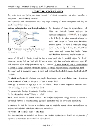
  • 1. Praveen Vaidya, Department of Physics, SDMCET, Dharwad-02 UNIT - III Page 1 of 11 SEMICONDUCTOR PHYSICS The solids those are having short-range symmetry of atomic arrangement are either crystalline or amorphous. These are mostly insulators. The conductors and semiconductors have long range symmetry of atomic arrangement and they are mostly in crystalline materials. Valance and conduction band in semiconductors: merger of 2N and 6N bands 2s and 2p into a single band with 8N available states. At effective interatomic spacing (ao), the band with 8N energy states, splits into two bands with energy states 4N each, separated by an energy gap or band gap Eg. Therefore, At zero K the Band Gap of a semiconductor is defined as Energy difference between the maxima of valency band and minima of conduction band. The upper band is conduction band, it is empty and the lower band called the valence band full with 4N electrons. For electric conduction, the electrons must transfer from valance band to conduction band; it is achieved by the application of sufficient energy to electrons in valance band. Band gap in insulators is high (Eg= 6 eV for carbon). Even at room temperature electrons cannot sufficient energy to excite into conduction band. For semiconductor bandgap is moderate; It is of the order of 1 eV. For Ex., Germanium – 0.66eV Silicon – 1.12 eV At 0K these materials are perfect insulators. But at higher temperature, energy available is sufficient to for valence electrons to cross this energy gap, reach conduction band and show some conductivity. In metals at 0k itself the electrons in conduction band or practically without external energy electron can move to the conduction band hence show some conductivity. Intrinsic and extrinsic semiconductors The semiconductors are classified into Intrinsic and extrinsic semiconductors based on the presence of impurities or dopants the basic distinctions are as follows. The formation of bands in semiconductors will follow the diamond (carbon) structure. Its electronic configuration is . It is a given in fig. 1. In the fig. taking interatomic distance on X-axis and Energy on Y-axis when interatomic distance reduces ( N atoms to form solid) energy levels 1s, 2s, and 2p split into, 2N, 2N, and 6N energy states and convert into bands. Further reduction in the interatomic spacing results into Fig. 1: The formation of energy bands is shown in above plot due to variation in Energy of levels against lattice constant (ao)
  • 2. Praveen Vaidya, Department of Physics, SDMCET, Dharwad-02 UNIT - III Page 2 of 11 DIFFERENCE BETWEEN INTRENSIC AND EXTRINSIC SEMICONDUCTORS: Extrinsic semiconductor : To enhance the conductivity of semiconductor the concentration of charge carriers are increased by adding some impurities. Extrinsic semiconductors are formed when a small proportion of of impurity atoms (about 1 in 106) are replaced by the atoms of pure (intrinsic) semiconductor crystals. The process of adding impurity to pure semiconductor is called as doping. Impurity is called as dopant. Extrinsic Semiconductors are classified into, 1) p-type and 2) n-type semiconductors resp. Depending on the type of carrier doped the semiconductors classified into two types those are, 1. p-type semiconductor in which trivalent impurity element is doped and 2. n-type semiconductor in which pentavalent impurity element is doped Position of Fermi energy in semiconductors: In case of semiconductors, the Fermi energy is defined as; the average of highest energies possessed by the electrons in solid at a given temperature is also called as Fermi energy, when related to semiconductors. DIFFERENCE INTRINSIC SEMICONDUCTOR p-type SEMICONDUCTOR n-type Semiconductor Presence of impurity The pure semiconducting materials without the doping of impurity. Formed by doping Group III element of periodic table like Al, Ga, In. Formed by doping Group V element of periodic table, impurity like P, As, Sb. Density of holes and electrons The number of free electrons in the conduction band is equal to the number of holes in the valence band at T>0K Holes are majority carriers and electrons are minority carriers. Electrons are majority carriers and Holes are minority carriers. Electrical conductivity Negligible conductivity as direction of motion of equal number of holes and electrons in opposite direction Conductivity is due to holes as they are majority carriers. Conductivity is high due to electrons as they are majority carriers. Conductivit y at 0k Conductivity is zero and act as perfect insulators Small amount of conductivity due to presence of impurity. Small amount of conductivity due to presence of impurity. Position of Fermi energy At the centre of Conduction band minimum and valance band maximum At centre of accepter level and valance band maximum At the centre of conduction band minimum and donor level.
  • 3. Praveen Vaidya, Department of Physics, SDMCET, Dharwad-02 UNIT - III Page 3 of 11 EC EF ED EV Conduction band Valence band n – type semiconductor EC EA EF EV Conduction band Valency band p – type semiconductor Fermi Energy in case of Intrinsic Semiconductors: Therefore the the Fermi energy of the intrinsic semiconductor is given by 2 V C F E E E   and EC – EF = Eg/2 Where Eg is the energy gap of semiconductor. Fermi energy in case of extrinsic semiconductors: a) In case of p-type semiconductors: An additional vacancy (hole) is generated by doping pure semiconductor with accepter type impurity. This hole has energy slightly greater than valence band maximum. This additional hole finds an energy level above the valance band. A new energy level is called as accepter level (EA). The energy of the intrinsic holes in the valency band have heighest energy EV, therefore the Fermi energy in p-type semiconductor is given by the average value of EA and EV. 2 A V F E E E   b) In case of n-type semiconductors: The impurity Electron generated by doping with doner type impurity is weakly bound to lattice. This electron has slightly less energy than that of electron in the lowest state of conduction band. Hence, this electron occupy in an energy level below the conduction band called as donor level (ED). Energy of the intrinsic electron in the conduction band have lowest energy EC, therefore the Fermi energy in n-type Eg EC EF EV Conduction band Valency band In case of intrinsic semiconductors, excited electrons possess highest energy at least at the bottom of conduction band and the electrons occupied vacant sites (holes) in valancy band having highest energy at least at the top of valence band. Hence to determine the Fermi energy one can consider the average value of energy possessed by electrons at the bottom of the conduction band (Ec) and energy possessed by electrons at the top of the valence band (Ev),
  • 4. Praveen Vaidya, Department of Physics, SDMCET, Dharwad-02 UNIT - III Page 4 of 11 semiconductor is average value of ED and EV. 2 D C F E E E   Classification of semiconductor on the basis of the Band gap The semiconductors are classified into two types on the basis of the bandgap. 1. Indirect Bandgap semiconductors 2. Direct Bandgap semiconductors 1. Indirect Bandgap Semiconductors: The semiconductor materials in which the maximum of valance band is not exactly below the minimum conduction band are called Indirect band gap semiconductors. It is shown in the E-k diagram (Fig. 2b). to valance band it given out phonon and reaches valance band maxima radiating heat or gives non- irradiative transition Therefore, indirect bandgap semiconductors are not suitable only for electrical properties. As biasing circuit of diodes, as rectifiers and switches etc. Examples of Indirect bandgap semiconductors are Silicon, Germanium. Tellurium GaP, SiC etc. 2. Direct Bandgap Semiconductors: The semiconductors in which maximum of valance band is exactly below the minimum conduction band to conserve energy and momentum are called as Direct bandgap semiconductors. (E-k diagram Fig.2a). When transition takes place from valance band to conduction band, by absorbing the photon, the energy as well as momentum are conserved, because the maxima of valance band and minima conduction band are in same ‘k’ value, similarly when transition takes place from conduction band to valance band electron give out the photon (electromagnetic radiation) of energy equivalent to that it absorbed without giving intermediate particle. Material Direct / Indirect Bandgap Band Gap Energy at 300 K (eV) Elements C (diamond) Ge Si Indirect Indirect Indirect 5.47 0.66 1.12 When transition takes place from valance band to conduction band by absorbing the photon, the energy is conserved but not momentum, because the maximum of valance band and minimum conduction band are not in same ‘k’ value, this is compensated by the quantum particle called phonon, therefore there is interaction of electron, photon and phonon. Similarly, when transition takes place from conduction band Fig 2a Fig 2b
  • 5. Praveen Vaidya, Department of Physics, SDMCET, Dharwad-02 UNIT - III Page 5 of 11 Groups III-V compounds GaAs InAs GaP GaN Direct Direct Indirect Direct 1.42 0.36 2.26 3.36 Groups II-VI compounds ZnO CdSe ZnS Direct Direct Direct 3.35 1.70 3.68 Examples of Direct band gap semiconductors are Compound semiconductors (The semiconductors formed by compsite of two or more elements) Like, Gallium Arsenide (GaAs), Cadmium Telluride (CdTe), Zinc Sulphide (ZnS), etc., The compound semiconductor are divided into III-V and II-VI semiconductor, in farmer the Group III and Group V elements are composed ( Ga and As – GaAs) and in later Group II and Group VI (Cd and Te – CdTe) elements of the periodic table composed to become semiconductor respectively. This combination is made because to get the semiconductors required bandgap and the higher bandgap semiconductors. The higher Direct bandgap semiconductors are emit the electromagnetic radiation in Near IR, Visible and in Ultra violet region. These semiconductors are highly useful in optoelectronic properties like in case producing Light emitting diods (LEDs), LASERs, Sensors and Solar Photovoltaic’s etc., GaAs is the semiconductor maximum used in satellite and space shuttle solar panel. Distinction between Direct Bandgap and Indirct bandgap Seemiconductors Sl. No. Direct Band gap semiconductor Indirect Band gap semiconductor 1 A direct band-gap (DBG) semiconductor is one in which the maximum energy level of the valence band aligns with the minimum energy level of the conduction band with respect to momentum. A indirect band-gap (IDBG) semiconductor is one in which the maximum energy level of the valence band are misaligned with the minimum energy level of the conduction band with respect to momentum. 2 In a DBG semiconductor, a direct recombination takes place with the release of the energy equal to the energy difference between the recombining particles Due to a relative difference in the momentum, first, the momentum is conserved by release of energy and only after both the momenta align themselves, a recombination occurs accompanied with the release of energy 3. The efficiency factor of a DBG semiconductor is much more than that of an IBG semiconductor The probability of a radiative recombination, is much less in comparison to that in case of DBG semiconductors 4 The most thoroughly investigated and studied DBG semiconductor material is Gallium Arsenide (GaAs). The two well-known intrinsic semiconductors, Silicon and Germanium are both IBG semiconductors
  • 6. Praveen Vaidya, Department of Physics, SDMCET, Dharwad-02 UNIT - III Page 6 of 11 5 DBG semiconductors are always preferred over IBG for making optical sources The IBG semiconductors cannot be used to manufacture optical sources. Carrier concentration in semiconductors It is known that electrons and holes are the current carriers in semiconductors. In case of intrinsic semiconductors, at temperature above 0 k, the electrons and holes are created as a pair due to breaking of bonds. This phenomenon is called electron hole pair generation. If ‘n’ is number of electrons per unit volume (electron density) in conduction band and ‘p’ is number holes per unit volume (hole density) in valance band, then n = p = ni The conductivity of semiconductor is go on increases as temperature increases, so one can find large number of electrons in conduction band and that of holes in valance band. The density of carriers can be found by using the theory of Fermi-dirac statistics, according which, Density of electrons in conduction band between the energy E (highest energy level occupied by electron) and EC (lowest energy of electron near conduction band) is given by, Where gc(E) is the density of states in the conduction band and f(E) is the Fermi function. Substituting the value of gc(E), f(E) and integrating we get, The electron concentration (no) is (taking E = ∞, represents the top of conduction band) ---(1) dE e E E m h kT E E E c e F C              2 / 3 3 2 8 dE e E E e m h kT E E E c kT E E e C C C F                     2 / 3 3 2 8 2 / 3 2 / 3 3 ) ( 2 2 8 kT e m h kT E E e C F                              kT E E e F C e h kT m 2 / 3 2 2 2  This can be written as          kT E E C F C e N - Electron carrier concentration.
  • 7. Praveen Vaidya, Department of Physics, SDMCET, Dharwad-02 UNIT - III Page 7 of 11 Where NC is given by, Similarly, density of holes in valance band is given by Fermi dirac distribution, Substituting the value of gc(E), f(E) and integrating we get, dE e E E m h p kT E E EV V h o F                1 1 1 2 8 2 / 3 3  dE e E E e m h kT E E E V kT E E h F V V F                       2 / 3 3 2 8 2 / 3 2 / 3 3 ) ( 2 2 8 kT e m h kT E E h V F                               kT E E h V F e h kT m 2 / 3 2 2 2  This can be written as          kT E E V V F e N - Hole carrier concentration Where In above equations of electron and hole concentration of a intrinsic semiconductors Where Nc and Nv are the temperature-dependent material constant known as the effective density of states in conduction band and valance band respectively. In the above two integrals, the actual location of the top of the conduction band/bottom of valance does not need to be known as the Fermi function goes to zero at higher energies in conduction band/lower inergies in valance band. Intrinsic carrier density: We know that, in intrinsic semiconductor, n = p = ni therefore, nopo = ni 2                  kT E E C i C F e N n 2                 kT E E V V F e N =         kT E E V C V C e N N ,
  • 8. Praveen Vaidya, Department of Physics, SDMCET, Dharwad-02 UNIT - III Page 8 of 11 but EC – EV = Eg           kT E V C i g e N N n 2 2 / 1 ) ( Substituting the values of NC and NV , 2 / 3 4 / 3 2 / 3 2 ) ( 2 2 T m m h k n h e i                    kT Eg e 2 The above equation gives the net carrier concentration in an intrinsic semiconductor. Where Nc(300 K) is the effective density of states at 300 K Mobility of charge carriers: At room temperature electrons semiconductor; excite to conduction band, leaving behind holes. Under the application electric field E, electrons and holes accelerate in opposite direction, hence drift velocity, ‘ q’ must be taken as n – for electrons and p – for holes. The ratio of the drift velocity to the applied electric field is known as mobility is given by For electrons in conduction band Electric Conductivity of Intrinsic Semiconductors: As per free electron theory, the conductivity σ of a metal is given by the expression, m ne   2  , but m e e    Therefore, σ = neμe Where n is the number of free electrons per unit volume of the conductor i.e. electron density, e is the electron charge and μe is the electron mobility. Conductivity due to electron in semiconducto is neμe Similarly, conductivity due to holes is peμh Since, in semiconductors the conduction is due to free electrons as well as holes. Electric conductivity of semiconductor is σ = σn + σp = neμe + peμh
  • 9. Praveen Vaidya, Department of Physics, SDMCET, Dharwad-02 UNIT - III Page 9 of 11 = e(nμe + pμh ) Since in intrinsic semiconductors n = p = ni, the intrinsic concentration of holes or free electron in the semiconductor. Therefore above equation takes the form, σ = nieμe + ni eμh So conductivity in intrinsic semiconductor. σ = nie (μe + μh ) HALL EFFECT: When a transverse magnetic field is applied to the conductor carrying current a voltage develop in the direction perpendicular to both direction of current and magnetic field respectively, is called as Hall Effect and voltage is called a Hall voltage. This phenomenon was discovered by E.H. Hall in 1879. Consider a specimen of conductor in the form thin strip with width (w) and thickness (d) and length (l). On application of electric field along length a current ‘I’ set up through the conductor. If the a magnetic field (B) applied in the direction thickness (d), then a potential difference (VH) developed in the direction of width (w) is measured with a millivoltmeter. In following figure, a conventional current flow along +ve X –axis (hence electron motion is along –ve X-axis) by the application electric field Ex and built current density Jx, on application Magnetic field along Z-axis (Bz), the electron experience transverse force called Lorentz force, is given by, F = – e (vx Bz) due to this force accumulation of charges at the ends of conductor, which builds electric field (Ey). along Y-axis, this electric force along Y-axis is given by, Fy = – e Ey Under equilibrium, these two forces balance each other is given by, Ey = vx Bz ═> vx = Ey/Bz
  • 10. Praveen Vaidya, Department of Physics, SDMCET, Dharwad-02 UNIT - III Page 10 of 11 The current density along X-direction is given by, Jx = – nevx ═> Jx = neEy /Bz H x y R z B J E ne    1 RH here is called as Hall coefficient. But, Ey = VH/w (w – width of the conductor) Therefore, J = – neVy/wBz or, ne z JwB ne z JwB H V     J = I/A = I/dxw, Therefore, dne z IB H V   VH is called as hall voltage. Where d and w are thickness and width of the sample perpendicular to direction of current. Importance of Hall Effect Measurements: # Invaluable for characterizing semiconductor materials, whether they are silicon-based, compound semiconductors, thin-film materials for solar cells, or nanoscale materials like graphene. #The measurements span low-resistance (highly doped semiconductors, high-temp. superconductors and GMR/ TMR materials and high-resistance semiconductors including semi-insulating GaAs, GAN etc. # Useful for determining various material parameters, but the primary one is the Hall voltage (VH). Carrier mobility, carrier concentration (n), Hall coefficient (RH) and the carrier types. As researchers develop next-generation ICs and more efficient semiconductor materials, they’re particularly interested in materials with high carrier mobility, which is what’s sparked much of the interest in graphene. This one atom-thick form of carbon exhibits the quantum Hall Effect and, as a result, relativistic electron current flow. Researchers consider Hall Effect measurements crucial to the future of the electronics industry.
  • 11. Praveen Vaidya, Department of Physics, SDMCET, Dharwad-02 UNIT - III Page 11 of 11 ] Fermi dirac statistics applied to semiconductors (Not for syllabus) The density of states in a semiconductor was obtained by solving the Schrödinger equation for the particles in the semiconductor. Rather than using the actual and very complex potential in the semiconductor, we use the simple particle-in-a box model, where one assumes that the particle is free to move within the material. For an electron which behaves as a free particle with effective mass, m* , the density of states was derived using, where Ec is the bottom of the conduction band below which the density of states is zero. The density of states for holes in the valence band is given by: The densityof electrons in a semiconductor is related to the densityof available statesand the probabilitythat each of these states is occupied. Questions: 1. Distinguish p-type and n-type semiconductors. 2. How the energy gap of semiconductor is different from its Fermi energy? 3. With a band diagram elucidate the position Fermi energy in intrinsic and extrinsic semiconductors. 4. What you mean by doping? Distinguish the semiconductors based on nature of dopant with diagram showing the band gap (Distinguish the intrinsic and extrinsic semiconductors) and Fermi level. 5 What are carriers related to semiconductors. Starting from the expression for the density of state and Fermi direct distribution, arrive at the expression for the effective density of states 6 Derive expressions for the intrinsic carrier concentration (ni) of semiconductor and show that ni independent of Fermi energy. 7 Derive an expression for the electric conductivity of a semiconductor in terms of carrier concentration and mobility. 8 Write any three applications of hall effect 9 Derive an expression for hall voltage and hall coefficient of a given conductor. The densityof occupied states per unit volume and energy, n(E), ), is simply the product of the density of states in the conduction band, gc(E) and the Fermi-Dirac probability function, f(E), (also called the Fermi function): Since holes correspond to empty states in the valence band, the probability of having a hole equals the probability that a particular state is not filled, so that the hole density per unit energy, p(E), equals: Where gv(E) is the densityof states in the valence band. The density of carriersis then obtained by integrating the density of carriers per unit energy over all possible energies within a band. A general expression is derived as well as an approximate analytic solution, which is valid for non-degenerate semiconductors. In addition, we also present the Joyce-Dixon approximation, an approximate solution useful when describing degenerate semiconductors.