SlideShare una empresa de Scribd logo
1 de 19
SEMICONDUCTOR FUNDAMENTALS
Free electron model that works well for metals do not apply for crystals. Free electrical
model gives us good insight into heat capacity, thermal conductivity, electron conductivity
& electrodynamics of metal; but it fails to answer other large question: distinction between
metals, semimetals, semiconductors & insulators; occurrence of positive values of Hall
coefficient & many detailed transport properties. The reason behind it is the periodicity of
the potential characterizing the crystal, whose value at any point is the result of
contributions from each atom. When atoms form crystals, presence of neighbouring atoms
does not affect the energy levels of inner shell electrons. However, the levels of outer shell
electrons are changed considerably, as the outer shell electrons are shared by more than
one atom in the crystal.
Quantum mechanics helps to find out the new energy levels of the outer electrons.
Coupling exists between the outer shell electrons of the atoms and is responsible for the
appearance of the band of closely spaced energy states, rather than widely separated
energy level as that of the isolated atoms. Regions in energy for which no wave like
electron orbital exists are called energy gaps or band gaps & results from the interaction of
the conduction electron wave with the ion cores of the crystal.
IVA,Group
Elements
Atomic
Number
Electronic configuration
C
Si
Ge
6
14
32
1s2 2s2 2p2
1s2 2s2 2p6 3s2 3p2
1s2 2s2 2p6 3s2 3p6 3d10 4s2 4p2
Each of the elements given above contains 2s electrons and 2p electron in the outer two
sub shells. If we ignore the inner shell levels, there are 2N electrons completely filling the
2N possible s levels all at same energy. Well known that p atomic sub shell has 6 possible
states, our crystal having widely spaced atoms (2N electrons), will fill only one third of
the 6N possible p states, all at the same level. Now if we decrease the interatomic spacing
of the crystal, each atom will experience an electric force from it’s neighbouring atoms.
This coupling between atoms gives rise to overlapping of atomic wave functions and
crystal becomes an electronic system which will obey Pauli exclusion principle. If
interatomic distance is decreased sufficiently, the total spread between the minimum and
maximum energy may be several electron volts, since N is very large (⋍1023cm-3),
although separation between levels is small.
These large numbers of discrete and closely spaced energy levels are called an energy band.
Now each atom has given up 4 electrons to the band at this particular spacing; which no
longer belongs to orbit in s or p sub shell of an isolated atom, but rather they belong to the
crystal as a whole. The band occupied by these electrons is called valence band. Valence
band filed with 4N electrons is separated by a forbidden band (EG) from an empty band
consisting of 4N additional states. This upper vacant band is called conduction band.
METALS, INSULATORS & SEMICONDUCTORS
A very poor conductor of electricity is called insulator, whereas good conductors of
electricity is called metal. Semiconductors are those substance whose conductivity lies
between these two extremes.
Energy band diagram give explanation for above three categories:-
Metal
Insulator
Semiconductor
Substance for which forbidden energy region is small enough i.e E𝐺 ⋍ 1 𝑒 𝑉, the externally
applied field may carry the particle from valence band to conduction band. These free or
conduction electrons participate in conductivity & substance now become slightly conducting;
it is a semiconductor. The most widely used semiconductor materials are germanium &
silicon having band gaps 0.785 and 1.21 eV respectively. Si atom has 14 protons and 14
electrons. 4valence electrons in outer most orbit indicates Si to be an semiconductor. These Si
atoms combine to form a crystal.
Each Si atom shares its 4 valence electrons
with the 4 neighbouring atoms in order to have
8 valence electrons in its valence orbit.
CLASSIFICATION OF SEMICONDUCTORS:
Conductivity of semiconductors lies in between 105 to 10-4 Siemens per meter. Since
semiconductors have negative coefficient of resistance; their resistance decreases with
increases in temperature. Other important property is that conductivity changes considerably
with addition of even small amount of substances called impurities are added to them.
Semiconductors are classified in following two ways – (a) Intrinsic semiconductor (b)
Extrinsic semiconductors.
COVALENT BONDS IN INTRINSIC SEMICONDUCTOR:
THE HOLE:
However, at room temperature some of the covalent bonds are broken due to the thermal
energy of the crystal causing atoms to vibrate. As a result, conduction is possible due to the
availability of charge carriers. The energy EG required to dislodge a valence electron of a
covalent bond & to make it free to participate in conduction is about 0.72eV for
germanium & 1.1eV for Silicon at room temperature. The absence of electron in covalent
bond is represented by a small circle & known as hole. Hole serves as a positive charge
carrier of electricity as effective as a free electron (negative charge).
FLOW OF HOLES:
Free electrons & holes move in opposite direction i.e. free electrons move towards left
along path D,C,B,A. and hole towards right along A,B,C,D,E,F,G acting the same as
positive charge.
EXTRINSIC SEMICONDUCTOR:
Intrinsic semiconductor have small conductivity at room temperature. In order to increase
the conductivity of intrinsic semiconductor a trivalent or pentavalent impurity is added to
the semiconductor. This process of adding trivalent or pentavalent impurity to the pure
semiconductor in order to increase the conductivity is called doping. Doping is done at the
rate such that only one atom of impurity is added per 106 to 1010 semiconductor atoms.
Charge carriers i.e. free electrons or holes can be increased, depending on the type of
impurity (pentavalent or trivalent) added.
DONOR IMPURITIES: (PENTA VALENT IMPURITIES):
0.05 eV for Si & 0.01 eV for Ge
ACCEPTOR IMPURITIES: (TRIVALENT IMPURITIES):
0.01 eV for Ge & 0.05eV for Si
Questions:
Q1. Explain with energy band diagram the difference between insulator, semiconductor and
metals..
Q2. Discuss and explain with diagram the difference between intrinsic and extrinsic
semiconductor.
Q3. Draw and explain the energy band diagram for n type and p type semiconductors.
Module 1  Semiconductors (1).pptx

Más contenido relacionado

Similar a Module 1 Semiconductors (1).pptx

Topic energy band gap material science ppt
Topic  energy band gap material science pptTopic  energy band gap material science ppt
Topic energy band gap material science pptSubhashYadav144
 
SEMICONDUCTORS ppt.pptx
SEMICONDUCTORS ppt.pptxSEMICONDUCTORS ppt.pptx
SEMICONDUCTORS ppt.pptxSayantaniBose2
 
Solids_And_Semiconductor_Devices_1.ppt
Solids_And_Semiconductor_Devices_1.pptSolids_And_Semiconductor_Devices_1.ppt
Solids_And_Semiconductor_Devices_1.pptssuserfa217a
 
Class 12th Solids and semiconductor devices part 1
Class 12th Solids and semiconductor devices part 1Class 12th Solids and semiconductor devices part 1
Class 12th Solids and semiconductor devices part 1Arpit Meena
 
Electronic device lecture1
Electronic device lecture1Electronic device lecture1
Electronic device lecture1Neeraj Gupta
 
Electronic device lecture1
Electronic device lecture1Electronic device lecture1
Electronic device lecture1Neeraj Gupta
 
UNIT 3 Analog Electronics.pptx
UNIT 3 Analog Electronics.pptxUNIT 3 Analog Electronics.pptx
UNIT 3 Analog Electronics.pptxDHARUNESHBOOPATHY
 
semiconductor and hall effect.pptx chemistry .....
semiconductor and hall effect.pptx chemistry .....semiconductor and hall effect.pptx chemistry .....
semiconductor and hall effect.pptx chemistry .....amruthatk3
 
Solids_And_Semiconductor_Devices_123.pdf
Solids_And_Semiconductor_Devices_123.pdfSolids_And_Semiconductor_Devices_123.pdf
Solids_And_Semiconductor_Devices_123.pdfanuragyadav8778
 
ENERGY BANDS AND EFFECTIVE MASSppt
ENERGY BANDS AND EFFECTIVE MASSpptENERGY BANDS AND EFFECTIVE MASSppt
ENERGY BANDS AND EFFECTIVE MASSpptBiswajeetMishra21
 
Class 12 th semiconductor part 1
Class 12 th semiconductor part 1Class 12 th semiconductor part 1
Class 12 th semiconductor part 1Priyanka Jakhar
 
Class 12 th semiconductor part 1
Class 12 th semiconductor part 1Class 12 th semiconductor part 1
Class 12 th semiconductor part 1Priyanka Jakhar
 
applied electronics 1
applied electronics 1applied electronics 1
applied electronics 1Tadesse6
 
Basic electronics
Basic electronicsBasic electronics
Basic electronicssuganyaaam
 

Similar a Module 1 Semiconductors (1).pptx (20)

Topic energy band gap material science ppt
Topic  energy band gap material science pptTopic  energy band gap material science ppt
Topic energy band gap material science ppt
 
SEMICONDUCTORS ppt.pptx
SEMICONDUCTORS ppt.pptxSEMICONDUCTORS ppt.pptx
SEMICONDUCTORS ppt.pptx
 
Solids_And_Semiconductor_Devices_1.ppt
Solids_And_Semiconductor_Devices_1.pptSolids_And_Semiconductor_Devices_1.ppt
Solids_And_Semiconductor_Devices_1.ppt
 
Class 12th Solids and semiconductor devices part 1
Class 12th Solids and semiconductor devices part 1Class 12th Solids and semiconductor devices part 1
Class 12th Solids and semiconductor devices part 1
 
Electronic device lecture1
Electronic device lecture1Electronic device lecture1
Electronic device lecture1
 
Electronic device lecture1
Electronic device lecture1Electronic device lecture1
Electronic device lecture1
 
Electronic device lecture1
Electronic device lecture1Electronic device lecture1
Electronic device lecture1
 
Energy bands and gaps in semiconductor
Energy bands and gaps in semiconductorEnergy bands and gaps in semiconductor
Energy bands and gaps in semiconductor
 
UNIT 3 Analog Electronics.pptx
UNIT 3 Analog Electronics.pptxUNIT 3 Analog Electronics.pptx
UNIT 3 Analog Electronics.pptx
 
semiconductor and hall effect.pptx chemistry .....
semiconductor and hall effect.pptx chemistry .....semiconductor and hall effect.pptx chemistry .....
semiconductor and hall effect.pptx chemistry .....
 
Solids_And_Semiconductor_Devices_123.pdf
Solids_And_Semiconductor_Devices_123.pdfSolids_And_Semiconductor_Devices_123.pdf
Solids_And_Semiconductor_Devices_123.pdf
 
ENERGY BANDS AND EFFECTIVE MASSppt
ENERGY BANDS AND EFFECTIVE MASSpptENERGY BANDS AND EFFECTIVE MASSppt
ENERGY BANDS AND EFFECTIVE MASSppt
 
Class 12 th semiconductor part 1
Class 12 th semiconductor part 1Class 12 th semiconductor part 1
Class 12 th semiconductor part 1
 
Class 12 th semiconductor part 1
Class 12 th semiconductor part 1Class 12 th semiconductor part 1
Class 12 th semiconductor part 1
 
applied electronics 1
applied electronics 1applied electronics 1
applied electronics 1
 
Bonding in metals
Bonding in metalsBonding in metals
Bonding in metals
 
Basic electronics
Basic electronicsBasic electronics
Basic electronics
 
Unit 3.docx
Unit 3.docxUnit 3.docx
Unit 3.docx
 
4. Semiconductors
4. Semiconductors4. Semiconductors
4. Semiconductors
 
Lecture-1.pdf
Lecture-1.pdfLecture-1.pdf
Lecture-1.pdf
 

Último

Sachpazis Costas: Geotechnical Engineering: A student's Perspective Introduction
Sachpazis Costas: Geotechnical Engineering: A student's Perspective IntroductionSachpazis Costas: Geotechnical Engineering: A student's Perspective Introduction
Sachpazis Costas: Geotechnical Engineering: A student's Perspective IntroductionDr.Costas Sachpazis
 
Electronically Controlled suspensions system .pdf
Electronically Controlled suspensions system .pdfElectronically Controlled suspensions system .pdf
Electronically Controlled suspensions system .pdfme23b1001
 
Call Girls Narol 7397865700 Independent Call Girls
Call Girls Narol 7397865700 Independent Call GirlsCall Girls Narol 7397865700 Independent Call Girls
Call Girls Narol 7397865700 Independent Call Girlsssuser7cb4ff
 
Why does (not) Kafka need fsync: Eliminating tail latency spikes caused by fsync
Why does (not) Kafka need fsync: Eliminating tail latency spikes caused by fsyncWhy does (not) Kafka need fsync: Eliminating tail latency spikes caused by fsync
Why does (not) Kafka need fsync: Eliminating tail latency spikes caused by fsyncssuser2ae721
 
Risk Assessment For Installation of Drainage Pipes.pdf
Risk Assessment For Installation of Drainage Pipes.pdfRisk Assessment For Installation of Drainage Pipes.pdf
Risk Assessment For Installation of Drainage Pipes.pdfROCENODodongVILLACER
 
Introduction to Machine Learning Unit-3 for II MECH
Introduction to Machine Learning Unit-3 for II MECHIntroduction to Machine Learning Unit-3 for II MECH
Introduction to Machine Learning Unit-3 for II MECHC Sai Kiran
 
Call Girls Delhi {Jodhpur} 9711199012 high profile service
Call Girls Delhi {Jodhpur} 9711199012 high profile serviceCall Girls Delhi {Jodhpur} 9711199012 high profile service
Call Girls Delhi {Jodhpur} 9711199012 high profile servicerehmti665
 
Oxy acetylene welding presentation note.
Oxy acetylene welding presentation note.Oxy acetylene welding presentation note.
Oxy acetylene welding presentation note.eptoze12
 
Architect Hassan Khalil Portfolio for 2024
Architect Hassan Khalil Portfolio for 2024Architect Hassan Khalil Portfolio for 2024
Architect Hassan Khalil Portfolio for 2024hassan khalil
 
IVE Industry Focused Event - Defence Sector 2024
IVE Industry Focused Event - Defence Sector 2024IVE Industry Focused Event - Defence Sector 2024
IVE Industry Focused Event - Defence Sector 2024Mark Billinghurst
 
Gfe Mayur Vihar Call Girls Service WhatsApp -> 9999965857 Available 24x7 ^ De...
Gfe Mayur Vihar Call Girls Service WhatsApp -> 9999965857 Available 24x7 ^ De...Gfe Mayur Vihar Call Girls Service WhatsApp -> 9999965857 Available 24x7 ^ De...
Gfe Mayur Vihar Call Girls Service WhatsApp -> 9999965857 Available 24x7 ^ De...srsj9000
 
INFLUENCE OF NANOSILICA ON THE PROPERTIES OF CONCRETE
INFLUENCE OF NANOSILICA ON THE PROPERTIES OF CONCRETEINFLUENCE OF NANOSILICA ON THE PROPERTIES OF CONCRETE
INFLUENCE OF NANOSILICA ON THE PROPERTIES OF CONCRETEroselinkalist12
 
Decoding Kotlin - Your guide to solving the mysterious in Kotlin.pptx
Decoding Kotlin - Your guide to solving the mysterious in Kotlin.pptxDecoding Kotlin - Your guide to solving the mysterious in Kotlin.pptx
Decoding Kotlin - Your guide to solving the mysterious in Kotlin.pptxJoão Esperancinha
 
Gurgaon ✡️9711147426✨Call In girls Gurgaon Sector 51 escort service
Gurgaon ✡️9711147426✨Call In girls Gurgaon Sector 51 escort serviceGurgaon ✡️9711147426✨Call In girls Gurgaon Sector 51 escort service
Gurgaon ✡️9711147426✨Call In girls Gurgaon Sector 51 escort servicejennyeacort
 
Study on Air-Water & Water-Water Heat Exchange in a Finned Tube Exchanger
Study on Air-Water & Water-Water Heat Exchange in a Finned Tube ExchangerStudy on Air-Water & Water-Water Heat Exchange in a Finned Tube Exchanger
Study on Air-Water & Water-Water Heat Exchange in a Finned Tube ExchangerAnamika Sarkar
 
Artificial-Intelligence-in-Electronics (K).pptx
Artificial-Intelligence-in-Electronics (K).pptxArtificial-Intelligence-in-Electronics (K).pptx
Artificial-Intelligence-in-Electronics (K).pptxbritheesh05
 
Correctly Loading Incremental Data at Scale
Correctly Loading Incremental Data at ScaleCorrectly Loading Incremental Data at Scale
Correctly Loading Incremental Data at ScaleAlluxio, Inc.
 
main PPT.pptx of girls hostel security using rfid
main PPT.pptx of girls hostel security using rfidmain PPT.pptx of girls hostel security using rfid
main PPT.pptx of girls hostel security using rfidNikhilNagaraju
 
Past, Present and Future of Generative AI
Past, Present and Future of Generative AIPast, Present and Future of Generative AI
Past, Present and Future of Generative AIabhishek36461
 

Último (20)

Sachpazis Costas: Geotechnical Engineering: A student's Perspective Introduction
Sachpazis Costas: Geotechnical Engineering: A student's Perspective IntroductionSachpazis Costas: Geotechnical Engineering: A student's Perspective Introduction
Sachpazis Costas: Geotechnical Engineering: A student's Perspective Introduction
 
Electronically Controlled suspensions system .pdf
Electronically Controlled suspensions system .pdfElectronically Controlled suspensions system .pdf
Electronically Controlled suspensions system .pdf
 
Call Girls Narol 7397865700 Independent Call Girls
Call Girls Narol 7397865700 Independent Call GirlsCall Girls Narol 7397865700 Independent Call Girls
Call Girls Narol 7397865700 Independent Call Girls
 
Why does (not) Kafka need fsync: Eliminating tail latency spikes caused by fsync
Why does (not) Kafka need fsync: Eliminating tail latency spikes caused by fsyncWhy does (not) Kafka need fsync: Eliminating tail latency spikes caused by fsync
Why does (not) Kafka need fsync: Eliminating tail latency spikes caused by fsync
 
Risk Assessment For Installation of Drainage Pipes.pdf
Risk Assessment For Installation of Drainage Pipes.pdfRisk Assessment For Installation of Drainage Pipes.pdf
Risk Assessment For Installation of Drainage Pipes.pdf
 
Introduction to Machine Learning Unit-3 for II MECH
Introduction to Machine Learning Unit-3 for II MECHIntroduction to Machine Learning Unit-3 for II MECH
Introduction to Machine Learning Unit-3 for II MECH
 
Call Girls Delhi {Jodhpur} 9711199012 high profile service
Call Girls Delhi {Jodhpur} 9711199012 high profile serviceCall Girls Delhi {Jodhpur} 9711199012 high profile service
Call Girls Delhi {Jodhpur} 9711199012 high profile service
 
Oxy acetylene welding presentation note.
Oxy acetylene welding presentation note.Oxy acetylene welding presentation note.
Oxy acetylene welding presentation note.
 
Design and analysis of solar grass cutter.pdf
Design and analysis of solar grass cutter.pdfDesign and analysis of solar grass cutter.pdf
Design and analysis of solar grass cutter.pdf
 
Architect Hassan Khalil Portfolio for 2024
Architect Hassan Khalil Portfolio for 2024Architect Hassan Khalil Portfolio for 2024
Architect Hassan Khalil Portfolio for 2024
 
IVE Industry Focused Event - Defence Sector 2024
IVE Industry Focused Event - Defence Sector 2024IVE Industry Focused Event - Defence Sector 2024
IVE Industry Focused Event - Defence Sector 2024
 
Gfe Mayur Vihar Call Girls Service WhatsApp -> 9999965857 Available 24x7 ^ De...
Gfe Mayur Vihar Call Girls Service WhatsApp -> 9999965857 Available 24x7 ^ De...Gfe Mayur Vihar Call Girls Service WhatsApp -> 9999965857 Available 24x7 ^ De...
Gfe Mayur Vihar Call Girls Service WhatsApp -> 9999965857 Available 24x7 ^ De...
 
INFLUENCE OF NANOSILICA ON THE PROPERTIES OF CONCRETE
INFLUENCE OF NANOSILICA ON THE PROPERTIES OF CONCRETEINFLUENCE OF NANOSILICA ON THE PROPERTIES OF CONCRETE
INFLUENCE OF NANOSILICA ON THE PROPERTIES OF CONCRETE
 
Decoding Kotlin - Your guide to solving the mysterious in Kotlin.pptx
Decoding Kotlin - Your guide to solving the mysterious in Kotlin.pptxDecoding Kotlin - Your guide to solving the mysterious in Kotlin.pptx
Decoding Kotlin - Your guide to solving the mysterious in Kotlin.pptx
 
Gurgaon ✡️9711147426✨Call In girls Gurgaon Sector 51 escort service
Gurgaon ✡️9711147426✨Call In girls Gurgaon Sector 51 escort serviceGurgaon ✡️9711147426✨Call In girls Gurgaon Sector 51 escort service
Gurgaon ✡️9711147426✨Call In girls Gurgaon Sector 51 escort service
 
Study on Air-Water & Water-Water Heat Exchange in a Finned Tube Exchanger
Study on Air-Water & Water-Water Heat Exchange in a Finned Tube ExchangerStudy on Air-Water & Water-Water Heat Exchange in a Finned Tube Exchanger
Study on Air-Water & Water-Water Heat Exchange in a Finned Tube Exchanger
 
Artificial-Intelligence-in-Electronics (K).pptx
Artificial-Intelligence-in-Electronics (K).pptxArtificial-Intelligence-in-Electronics (K).pptx
Artificial-Intelligence-in-Electronics (K).pptx
 
Correctly Loading Incremental Data at Scale
Correctly Loading Incremental Data at ScaleCorrectly Loading Incremental Data at Scale
Correctly Loading Incremental Data at Scale
 
main PPT.pptx of girls hostel security using rfid
main PPT.pptx of girls hostel security using rfidmain PPT.pptx of girls hostel security using rfid
main PPT.pptx of girls hostel security using rfid
 
Past, Present and Future of Generative AI
Past, Present and Future of Generative AIPast, Present and Future of Generative AI
Past, Present and Future of Generative AI
 

Module 1 Semiconductors (1).pptx

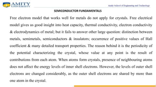
  • 1. SEMICONDUCTOR FUNDAMENTALS Free electron model that works well for metals do not apply for crystals. Free electrical model gives us good insight into heat capacity, thermal conductivity, electron conductivity & electrodynamics of metal; but it fails to answer other large question: distinction between metals, semimetals, semiconductors & insulators; occurrence of positive values of Hall coefficient & many detailed transport properties. The reason behind it is the periodicity of the potential characterizing the crystal, whose value at any point is the result of contributions from each atom. When atoms form crystals, presence of neighbouring atoms does not affect the energy levels of inner shell electrons. However, the levels of outer shell electrons are changed considerably, as the outer shell electrons are shared by more than one atom in the crystal.
  • 2. Quantum mechanics helps to find out the new energy levels of the outer electrons. Coupling exists between the outer shell electrons of the atoms and is responsible for the appearance of the band of closely spaced energy states, rather than widely separated energy level as that of the isolated atoms. Regions in energy for which no wave like electron orbital exists are called energy gaps or band gaps & results from the interaction of the conduction electron wave with the ion cores of the crystal.
  • 3. IVA,Group Elements Atomic Number Electronic configuration C Si Ge 6 14 32 1s2 2s2 2p2 1s2 2s2 2p6 3s2 3p2 1s2 2s2 2p6 3s2 3p6 3d10 4s2 4p2
  • 4. Each of the elements given above contains 2s electrons and 2p electron in the outer two sub shells. If we ignore the inner shell levels, there are 2N electrons completely filling the 2N possible s levels all at same energy. Well known that p atomic sub shell has 6 possible states, our crystal having widely spaced atoms (2N electrons), will fill only one third of the 6N possible p states, all at the same level. Now if we decrease the interatomic spacing of the crystal, each atom will experience an electric force from it’s neighbouring atoms. This coupling between atoms gives rise to overlapping of atomic wave functions and crystal becomes an electronic system which will obey Pauli exclusion principle. If interatomic distance is decreased sufficiently, the total spread between the minimum and maximum energy may be several electron volts, since N is very large (⋍1023cm-3), although separation between levels is small.
  • 5. These large numbers of discrete and closely spaced energy levels are called an energy band.
  • 6. Now each atom has given up 4 electrons to the band at this particular spacing; which no longer belongs to orbit in s or p sub shell of an isolated atom, but rather they belong to the crystal as a whole. The band occupied by these electrons is called valence band. Valence band filed with 4N electrons is separated by a forbidden band (EG) from an empty band consisting of 4N additional states. This upper vacant band is called conduction band. METALS, INSULATORS & SEMICONDUCTORS A very poor conductor of electricity is called insulator, whereas good conductors of electricity is called metal. Semiconductors are those substance whose conductivity lies between these two extremes.
  • 7. Energy band diagram give explanation for above three categories:- Metal Insulator Semiconductor
  • 8. Substance for which forbidden energy region is small enough i.e E𝐺 ⋍ 1 𝑒 𝑉, the externally applied field may carry the particle from valence band to conduction band. These free or conduction electrons participate in conductivity & substance now become slightly conducting; it is a semiconductor. The most widely used semiconductor materials are germanium & silicon having band gaps 0.785 and 1.21 eV respectively. Si atom has 14 protons and 14 electrons. 4valence electrons in outer most orbit indicates Si to be an semiconductor. These Si atoms combine to form a crystal. Each Si atom shares its 4 valence electrons with the 4 neighbouring atoms in order to have 8 valence electrons in its valence orbit.
  • 9. CLASSIFICATION OF SEMICONDUCTORS: Conductivity of semiconductors lies in between 105 to 10-4 Siemens per meter. Since semiconductors have negative coefficient of resistance; their resistance decreases with increases in temperature. Other important property is that conductivity changes considerably with addition of even small amount of substances called impurities are added to them. Semiconductors are classified in following two ways – (a) Intrinsic semiconductor (b) Extrinsic semiconductors.
  • 10. COVALENT BONDS IN INTRINSIC SEMICONDUCTOR:
  • 12. However, at room temperature some of the covalent bonds are broken due to the thermal energy of the crystal causing atoms to vibrate. As a result, conduction is possible due to the availability of charge carriers. The energy EG required to dislodge a valence electron of a covalent bond & to make it free to participate in conduction is about 0.72eV for germanium & 1.1eV for Silicon at room temperature. The absence of electron in covalent bond is represented by a small circle & known as hole. Hole serves as a positive charge carrier of electricity as effective as a free electron (negative charge).
  • 13. FLOW OF HOLES: Free electrons & holes move in opposite direction i.e. free electrons move towards left along path D,C,B,A. and hole towards right along A,B,C,D,E,F,G acting the same as positive charge.
  • 14. EXTRINSIC SEMICONDUCTOR: Intrinsic semiconductor have small conductivity at room temperature. In order to increase the conductivity of intrinsic semiconductor a trivalent or pentavalent impurity is added to the semiconductor. This process of adding trivalent or pentavalent impurity to the pure semiconductor in order to increase the conductivity is called doping. Doping is done at the rate such that only one atom of impurity is added per 106 to 1010 semiconductor atoms. Charge carriers i.e. free electrons or holes can be increased, depending on the type of impurity (pentavalent or trivalent) added.
  • 15. DONOR IMPURITIES: (PENTA VALENT IMPURITIES): 0.05 eV for Si & 0.01 eV for Ge
  • 16. ACCEPTOR IMPURITIES: (TRIVALENT IMPURITIES): 0.01 eV for Ge & 0.05eV for Si
  • 17. Questions: Q1. Explain with energy band diagram the difference between insulator, semiconductor and metals.. Q2. Discuss and explain with diagram the difference between intrinsic and extrinsic semiconductor. Q3. Draw and explain the energy band diagram for n type and p type semiconductors.