SlideShare una empresa de Scribd logo
1 de 23
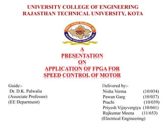
Guide:-
Dr. D.K. Palwalia
(Associate Professor)
(EE Department)
Delivered by:-
Nisha Verma (10/034)
Pawan Garg (10/037)
Prachi (10/039)
Priyesh Vijayvergiya (10/041)
Rajkumar Meena (11/653)
(Electrical Engineering)
UNIVERSITY COLLEGE OF ENGINEERING
RAJASTHAN TECHNICAL UNIVERSITY, KOTA
A
PRESENTATION
ON
APPLICATION OF FPGA FOR
SPEED CONTROL OF MOTOR
1. FPGA-Introduction
2. Why do we need FPGA
3. Structure of FPGA (Xilinx)
5. Nomenclature
6. Spartan 6 FPGA Kit – XC6SLX25-FT256
7. FPGA Programming
8. IPM – Intelligent Power Module
9. FPGA + IPM + MOTOR
10. Waveform observed
11. Applications of FPGA
12. Conclusion
13. References
 FPGA chips handle dense logic and memory elements offering very high logic capacity
 Uncommitted logic blocks are replicated in an FPGA with interconnects and I/O blocks
 A field-programmable gate array (FPGA) is an integrated circuit designed to
be configured by a customer or a designer after manufacturing – hence "field-
programmable
 FPGA’s contain lots of building blocks (ports, logic, …) with a complete
interconnection structure . By programming these connections, different logical
blocks or slices can be linked to obtain the desired circuit.
 The FPGA industry sprouted from programmable read-only memory (PROM) and
programmable logic devices (PLDs). Xilinx and Altera are the current FPGA market
leaders .
Before Programmable Logic?
 Fixed hardware = Fixed usability
 Limited flexibility only possible by adding software support, for example
processors.
 Upgrade or alteration in hardware logic was not guaranteed.
 An upgrade meant a completely new system.
With FPGAs
 Reprogrammable Logic reusability
 Lower Non-Recurring Engineering (NRE) Cost
 Good for Prototyping
 Less Time to Market
 Can act as a testing device for other digital circuits
 Economical to be used for small volumes of products
 Students can understand digital design concepts in a better way by designing their
custom logic
Logic Block
I/O Block
Interconnect
XC6SLX25-FT256
DEVICE
TYPE
PACKAGE
TYPE
NUMBER OF
PINS
X 1000=No. of
logic Gates
 To define the behavior of the FPGA, the user provides a hardware
description language (HDL) or a schematic design. The HDL form is
more suited to work with large structures because it's possible to
just specify them numerically rather than having to draw every piece
by hand.
 VHDL (VHSIC Hardware Description Language) is a hardware
description language used in electronic design automation to
describe digital and mixed-signal systems such as field-
programmable gate arrays and integrated circuits. VHDL can also be
used as a general purpose parallel programming language.
Step - by - Step Process
Choice of language (Verilog, VHDL)
Architectural design
Editing programs
Compiling programs
Synthesizing programs (.EDIF)
Placing and routing programs (.VO, .SDF, .TTF)
Loading programs to FPGA
Debugging FPGA programs
Documenting programs
Delivering programs
• It work as DC-DC Converter (Chopper) or DC-AC Converter (Inverter).
It works using a IGBT based IPM and works on basis of software from
DSP Processor. The power module can be used for studying the operation
of chopper, single phase and three phase inverter and speed control of
single phase and three phase induction motor , etc.
• They are advanced hybrid power devices that combine high speed, low
loss IGBTs with optimized gate drive and protection circuitry. Highly
effective over-current and short-circuit protection is realized through the
use of advanced current sense IGBT chips that allow continuous monitoring
of power device current.
• IPM has been optimized for minimum switching losses in order to meet
industry demands for acoustically noiseless inverters with carrier
frequencies up to 20KHz.
IPM
Output of PWM 1 and PWM 2
Output of PWM 3 and PWM 4
Output of PWM 5 and PWM 6
Output of I-1, I-2 and I-3 Pins
Output of I-4, I-5 and I-6.
06
Output of I-7, I-8 and I-9.
1. ASIC Prototyping
2. Automotive
3. Broadcast:
4. Consumer Electronics
5. Distributed Monetary Systems
6. Data Center
7. High Performance Computing
8. Industrial
9. Medical
10. Scientific Instruments
11. Security
12. Video & Image Processing
13. Wired Communication
14. Wireless Communication
The flexibility of FPGAs gives them a distinct advantage over other
programmable logic devices on the market. The advantage is most
apparent in application where time to market concerns are paramount.
Because FPGAs are reprogrammable and can implement any sort of logic
circuit, designs can be modified after initial implementation. With one
time programmable technologies such as AISCs, logic is set at the factory
and no changes can be made after manufacture . The drawbacks to FPGA
use involve speed and space. Switching gate resistances and capacitances
make for slow logic and poor logic density.
1. www.optimagic.com
2. Brown 1992, Field Programmable Gate Arrays, Kluwer Academic Publishers
3. Bostock 1996, FPGAs and Programmable LSI: a Designers Handbook, Oxford:
Butterworth-Hieneman
4. Wakerly 2000, Digital Design: Principals and Practice
5. www.xilinx.com
QUERIES ???

Más contenido relacionado

La actualidad más candente

FPGA Overview
FPGA OverviewFPGA Overview
FPGA OverviewMetalMath
 
Traditional vs. SoC FPGA Design Flow A Video Pipeline Case Study
Traditional vs. SoC FPGA Design Flow A Video Pipeline Case StudyTraditional vs. SoC FPGA Design Flow A Video Pipeline Case Study
Traditional vs. SoC FPGA Design Flow A Video Pipeline Case StudyAltera Corporation
 
Cnx corporate
Cnx corporateCnx corporate
Cnx corporateCONNEXIUM
 
Digital VLSI Design and FPGA Implementation
Digital VLSI Design and FPGA ImplementationDigital VLSI Design and FPGA Implementation
Digital VLSI Design and FPGA ImplementationAmber Bhaumik
 
FPGA Intro
FPGA IntroFPGA Intro
FPGA Intronaito88
 
Implementation of DSP Algorithms on FPGA
Implementation of DSP Algorithms on FPGAImplementation of DSP Algorithms on FPGA
Implementation of DSP Algorithms on FPGASilicon Mentor
 
Cpld and fpga mod vi
Cpld and fpga   mod viCpld and fpga   mod vi
Cpld and fpga mod viAgi George
 
Seminar on field programmable gate array
Seminar on field programmable gate arraySeminar on field programmable gate array
Seminar on field programmable gate arraySaransh Choudhary
 
4.FPGA for dummies: Design Flow
4.FPGA for dummies: Design Flow4.FPGA for dummies: Design Flow
4.FPGA for dummies: Design FlowMaurizio Donna
 
Reconfigurable ICs
Reconfigurable ICsReconfigurable ICs
Reconfigurable ICsAnish Goel
 
FROM FPGA TO ASIC IMPLEMENTATION OF AN OPENRISC BASED SOC FOR VOIP APPLICATION
FROM FPGA TO ASIC IMPLEMENTATION OF AN OPENRISC BASED SOC FOR VOIP APPLICATIONFROM FPGA TO ASIC IMPLEMENTATION OF AN OPENRISC BASED SOC FOR VOIP APPLICATION
FROM FPGA TO ASIC IMPLEMENTATION OF AN OPENRISC BASED SOC FOR VOIP APPLICATIONieijjournal
 

La actualidad más candente (20)

CPLD xc9500
CPLD xc9500CPLD xc9500
CPLD xc9500
 
FPGA Overview
FPGA OverviewFPGA Overview
FPGA Overview
 
Fpga
FpgaFpga
Fpga
 
Traditional vs. SoC FPGA Design Flow A Video Pipeline Case Study
Traditional vs. SoC FPGA Design Flow A Video Pipeline Case StudyTraditional vs. SoC FPGA Design Flow A Video Pipeline Case Study
Traditional vs. SoC FPGA Design Flow A Video Pipeline Case Study
 
Cnx corporate
Cnx corporateCnx corporate
Cnx corporate
 
Unit VI CPLD-FPGA Architecture
Unit VI CPLD-FPGA ArchitectureUnit VI CPLD-FPGA Architecture
Unit VI CPLD-FPGA Architecture
 
Digital VLSI Design and FPGA Implementation
Digital VLSI Design and FPGA ImplementationDigital VLSI Design and FPGA Implementation
Digital VLSI Design and FPGA Implementation
 
Introduction to FPGAs
Introduction to FPGAsIntroduction to FPGAs
Introduction to FPGAs
 
Session 2,3 FPGAs
Session 2,3 FPGAsSession 2,3 FPGAs
Session 2,3 FPGAs
 
FPGA Intro
FPGA IntroFPGA Intro
FPGA Intro
 
#EEE - Field programmable gate array
#EEE - Field programmable gate array#EEE - Field programmable gate array
#EEE - Field programmable gate array
 
FIELD PROGRAMMABLE GATE ARRAYS AND THEIR APPLICATIONS
FIELD PROGRAMMABLE GATE ARRAYS AND THEIR APPLICATIONSFIELD PROGRAMMABLE GATE ARRAYS AND THEIR APPLICATIONS
FIELD PROGRAMMABLE GATE ARRAYS AND THEIR APPLICATIONS
 
Implementation of DSP Algorithms on FPGA
Implementation of DSP Algorithms on FPGAImplementation of DSP Algorithms on FPGA
Implementation of DSP Algorithms on FPGA
 
Cpld and fpga mod vi
Cpld and fpga   mod viCpld and fpga   mod vi
Cpld and fpga mod vi
 
Seminar on field programmable gate array
Seminar on field programmable gate arraySeminar on field programmable gate array
Seminar on field programmable gate array
 
Fpga & VHDL
Fpga & VHDLFpga & VHDL
Fpga & VHDL
 
4.FPGA for dummies: Design Flow
4.FPGA for dummies: Design Flow4.FPGA for dummies: Design Flow
4.FPGA for dummies: Design Flow
 
Lecture syn 024.cpld-fpga
Lecture syn 024.cpld-fpgaLecture syn 024.cpld-fpga
Lecture syn 024.cpld-fpga
 
Reconfigurable ICs
Reconfigurable ICsReconfigurable ICs
Reconfigurable ICs
 
FROM FPGA TO ASIC IMPLEMENTATION OF AN OPENRISC BASED SOC FOR VOIP APPLICATION
FROM FPGA TO ASIC IMPLEMENTATION OF AN OPENRISC BASED SOC FOR VOIP APPLICATIONFROM FPGA TO ASIC IMPLEMENTATION OF AN OPENRISC BASED SOC FOR VOIP APPLICATION
FROM FPGA TO ASIC IMPLEMENTATION OF AN OPENRISC BASED SOC FOR VOIP APPLICATION
 

Similar a FPGAPpr_final

FROM FPGA TO ASIC IMPLEMENTATION OF AN OPENRISC BASED SOC FOR VOIP APPLICATION
FROM FPGA TO ASIC IMPLEMENTATION OF AN OPENRISC BASED SOC FOR VOIP APPLICATIONFROM FPGA TO ASIC IMPLEMENTATION OF AN OPENRISC BASED SOC FOR VOIP APPLICATION
FROM FPGA TO ASIC IMPLEMENTATION OF AN OPENRISC BASED SOC FOR VOIP APPLICATIONieijjournal1
 
FROM FPGA TO ASIC IMPLEMENTATION OF AN OPENRISC BASED SOC FOR VOIP APPLICATION
FROM FPGA TO ASIC IMPLEMENTATION OF AN OPENRISC BASED SOC FOR VOIP APPLICATIONFROM FPGA TO ASIC IMPLEMENTATION OF AN OPENRISC BASED SOC FOR VOIP APPLICATION
FROM FPGA TO ASIC IMPLEMENTATION OF AN OPENRISC BASED SOC FOR VOIP APPLICATIONieijjournal
 
System designing and modelling using fpga
System designing and modelling using fpgaSystem designing and modelling using fpga
System designing and modelling using fpgaIAEME Publication
 
Introduction to FPGA, VHDL
Introduction to FPGA, VHDL  Introduction to FPGA, VHDL
Introduction to FPGA, VHDL Amr Rashed
 
Nt1310 Unit 5 Algorithm
Nt1310 Unit 5 AlgorithmNt1310 Unit 5 Algorithm
Nt1310 Unit 5 AlgorithmAngie Lee
 
Fpga architectures and applications
Fpga architectures and applicationsFpga architectures and applications
Fpga architectures and applicationsSudhanshu Janwadkar
 
FPGA Architecture and application
FPGA Architecture and application FPGA Architecture and application
FPGA Architecture and application ADARSHJKALATHIL
 
Project report of 2016 Trainee_final
Project report of 2016 Trainee_finalProject report of 2016 Trainee_final
Project report of 2016 Trainee_finalAkash Chowdhury
 
FPGA in outer space seminar report
FPGA in outer space seminar reportFPGA in outer space seminar report
FPGA in outer space seminar reportrahul kumar verma
 
L12 programmable+logic+devices+(pld)
L12 programmable+logic+devices+(pld)L12 programmable+logic+devices+(pld)
L12 programmable+logic+devices+(pld)NAGASAI547
 
Design and Development of Artix-7 FPGAbased Educational Board
Design and Development of Artix-7 FPGAbased Educational BoardDesign and Development of Artix-7 FPGAbased Educational Board
Design and Development of Artix-7 FPGAbased Educational BoardIJERA Editor
 
L12_PROGRAMMABLE+LOGIC+DEVICES+(PLD).ppt
L12_PROGRAMMABLE+LOGIC+DEVICES+(PLD).pptL12_PROGRAMMABLE+LOGIC+DEVICES+(PLD).ppt
L12_PROGRAMMABLE+LOGIC+DEVICES+(PLD).pptMikeTango5
 
Programmable logic controller performance enhancement by field programmable g...
Programmable logic controller performance enhancement by field programmable g...Programmable logic controller performance enhancement by field programmable g...
Programmable logic controller performance enhancement by field programmable g...ISA Interchange
 
FPGAs – CHRONOLOGICAL DEVELOPMENTS AND CHALLENGES
FPGAs – CHRONOLOGICAL DEVELOPMENTS AND CHALLENGESFPGAs – CHRONOLOGICAL DEVELOPMENTS AND CHALLENGES
FPGAs – CHRONOLOGICAL DEVELOPMENTS AND CHALLENGESIAEME Publication
 
Final presentation [dissertation project], 20192 esv0002
Final presentation [dissertation project], 20192 esv0002Final presentation [dissertation project], 20192 esv0002
Final presentation [dissertation project], 20192 esv0002MOHAMMED FURQHAN
 
1. FPGA architectures.pdf
1. FPGA architectures.pdf1. FPGA architectures.pdf
1. FPGA architectures.pdfTesfuFiseha1
 

Similar a FPGAPpr_final (20)

FROM FPGA TO ASIC IMPLEMENTATION OF AN OPENRISC BASED SOC FOR VOIP APPLICATION
FROM FPGA TO ASIC IMPLEMENTATION OF AN OPENRISC BASED SOC FOR VOIP APPLICATIONFROM FPGA TO ASIC IMPLEMENTATION OF AN OPENRISC BASED SOC FOR VOIP APPLICATION
FROM FPGA TO ASIC IMPLEMENTATION OF AN OPENRISC BASED SOC FOR VOIP APPLICATION
 
FROM FPGA TO ASIC IMPLEMENTATION OF AN OPENRISC BASED SOC FOR VOIP APPLICATION
FROM FPGA TO ASIC IMPLEMENTATION OF AN OPENRISC BASED SOC FOR VOIP APPLICATIONFROM FPGA TO ASIC IMPLEMENTATION OF AN OPENRISC BASED SOC FOR VOIP APPLICATION
FROM FPGA TO ASIC IMPLEMENTATION OF AN OPENRISC BASED SOC FOR VOIP APPLICATION
 
Fpg as 11 body
Fpg as 11 bodyFpg as 11 body
Fpg as 11 body
 
ASIC VS FPGA.ppt
ASIC VS FPGA.pptASIC VS FPGA.ppt
ASIC VS FPGA.ppt
 
System designing and modelling using fpga
System designing and modelling using fpgaSystem designing and modelling using fpga
System designing and modelling using fpga
 
Introduction to FPGA, VHDL
Introduction to FPGA, VHDL  Introduction to FPGA, VHDL
Introduction to FPGA, VHDL
 
Nt1310 Unit 5 Algorithm
Nt1310 Unit 5 AlgorithmNt1310 Unit 5 Algorithm
Nt1310 Unit 5 Algorithm
 
4_BIT_ALU
4_BIT_ALU4_BIT_ALU
4_BIT_ALU
 
Fpga architectures and applications
Fpga architectures and applicationsFpga architectures and applications
Fpga architectures and applications
 
FPGA Architecture and application
FPGA Architecture and application FPGA Architecture and application
FPGA Architecture and application
 
Chapter 4
Chapter 4Chapter 4
Chapter 4
 
Project report of 2016 Trainee_final
Project report of 2016 Trainee_finalProject report of 2016 Trainee_final
Project report of 2016 Trainee_final
 
FPGA in outer space seminar report
FPGA in outer space seminar reportFPGA in outer space seminar report
FPGA in outer space seminar report
 
L12 programmable+logic+devices+(pld)
L12 programmable+logic+devices+(pld)L12 programmable+logic+devices+(pld)
L12 programmable+logic+devices+(pld)
 
Design and Development of Artix-7 FPGAbased Educational Board
Design and Development of Artix-7 FPGAbased Educational BoardDesign and Development of Artix-7 FPGAbased Educational Board
Design and Development of Artix-7 FPGAbased Educational Board
 
L12_PROGRAMMABLE+LOGIC+DEVICES+(PLD).ppt
L12_PROGRAMMABLE+LOGIC+DEVICES+(PLD).pptL12_PROGRAMMABLE+LOGIC+DEVICES+(PLD).ppt
L12_PROGRAMMABLE+LOGIC+DEVICES+(PLD).ppt
 
Programmable logic controller performance enhancement by field programmable g...
Programmable logic controller performance enhancement by field programmable g...Programmable logic controller performance enhancement by field programmable g...
Programmable logic controller performance enhancement by field programmable g...
 
FPGAs – CHRONOLOGICAL DEVELOPMENTS AND CHALLENGES
FPGAs – CHRONOLOGICAL DEVELOPMENTS AND CHALLENGESFPGAs – CHRONOLOGICAL DEVELOPMENTS AND CHALLENGES
FPGAs – CHRONOLOGICAL DEVELOPMENTS AND CHALLENGES
 
Final presentation [dissertation project], 20192 esv0002
Final presentation [dissertation project], 20192 esv0002Final presentation [dissertation project], 20192 esv0002
Final presentation [dissertation project], 20192 esv0002
 
1. FPGA architectures.pdf
1. FPGA architectures.pdf1. FPGA architectures.pdf
1. FPGA architectures.pdf
 

FPGAPpr_final

  • 1. Guide:- Dr. D.K. Palwalia (Associate Professor) (EE Department) Delivered by:- Nisha Verma (10/034) Pawan Garg (10/037) Prachi (10/039) Priyesh Vijayvergiya (10/041) Rajkumar Meena (11/653) (Electrical Engineering) UNIVERSITY COLLEGE OF ENGINEERING RAJASTHAN TECHNICAL UNIVERSITY, KOTA A PRESENTATION ON APPLICATION OF FPGA FOR SPEED CONTROL OF MOTOR
  • 2. 1. FPGA-Introduction 2. Why do we need FPGA 3. Structure of FPGA (Xilinx) 5. Nomenclature 6. Spartan 6 FPGA Kit – XC6SLX25-FT256 7. FPGA Programming 8. IPM – Intelligent Power Module 9. FPGA + IPM + MOTOR 10. Waveform observed 11. Applications of FPGA 12. Conclusion 13. References
  • 3.  FPGA chips handle dense logic and memory elements offering very high logic capacity  Uncommitted logic blocks are replicated in an FPGA with interconnects and I/O blocks  A field-programmable gate array (FPGA) is an integrated circuit designed to be configured by a customer or a designer after manufacturing – hence "field- programmable  FPGA’s contain lots of building blocks (ports, logic, …) with a complete interconnection structure . By programming these connections, different logical blocks or slices can be linked to obtain the desired circuit.  The FPGA industry sprouted from programmable read-only memory (PROM) and programmable logic devices (PLDs). Xilinx and Altera are the current FPGA market leaders .
  • 4. Before Programmable Logic?  Fixed hardware = Fixed usability  Limited flexibility only possible by adding software support, for example processors.  Upgrade or alteration in hardware logic was not guaranteed.  An upgrade meant a completely new system. With FPGAs  Reprogrammable Logic reusability  Lower Non-Recurring Engineering (NRE) Cost  Good for Prototyping  Less Time to Market  Can act as a testing device for other digital circuits  Economical to be used for small volumes of products  Students can understand digital design concepts in a better way by designing their custom logic
  • 7.
  • 8.  To define the behavior of the FPGA, the user provides a hardware description language (HDL) or a schematic design. The HDL form is more suited to work with large structures because it's possible to just specify them numerically rather than having to draw every piece by hand.  VHDL (VHSIC Hardware Description Language) is a hardware description language used in electronic design automation to describe digital and mixed-signal systems such as field- programmable gate arrays and integrated circuits. VHDL can also be used as a general purpose parallel programming language.
  • 9. Step - by - Step Process Choice of language (Verilog, VHDL) Architectural design Editing programs Compiling programs Synthesizing programs (.EDIF) Placing and routing programs (.VO, .SDF, .TTF) Loading programs to FPGA Debugging FPGA programs Documenting programs Delivering programs
  • 10.
  • 11. • It work as DC-DC Converter (Chopper) or DC-AC Converter (Inverter). It works using a IGBT based IPM and works on basis of software from DSP Processor. The power module can be used for studying the operation of chopper, single phase and three phase inverter and speed control of single phase and three phase induction motor , etc. • They are advanced hybrid power devices that combine high speed, low loss IGBTs with optimized gate drive and protection circuitry. Highly effective over-current and short-circuit protection is realized through the use of advanced current sense IGBT chips that allow continuous monitoring of power device current. • IPM has been optimized for minimum switching losses in order to meet industry demands for acoustically noiseless inverters with carrier frequencies up to 20KHz. IPM
  • 12.
  • 13. Output of PWM 1 and PWM 2
  • 14. Output of PWM 3 and PWM 4
  • 15. Output of PWM 5 and PWM 6
  • 16. Output of I-1, I-2 and I-3 Pins
  • 17. Output of I-4, I-5 and I-6.
  • 18. 06 Output of I-7, I-8 and I-9.
  • 19. 1. ASIC Prototyping 2. Automotive 3. Broadcast: 4. Consumer Electronics 5. Distributed Monetary Systems 6. Data Center 7. High Performance Computing 8. Industrial 9. Medical 10. Scientific Instruments 11. Security 12. Video & Image Processing 13. Wired Communication 14. Wireless Communication
  • 20. The flexibility of FPGAs gives them a distinct advantage over other programmable logic devices on the market. The advantage is most apparent in application where time to market concerns are paramount. Because FPGAs are reprogrammable and can implement any sort of logic circuit, designs can be modified after initial implementation. With one time programmable technologies such as AISCs, logic is set at the factory and no changes can be made after manufacture . The drawbacks to FPGA use involve speed and space. Switching gate resistances and capacitances make for slow logic and poor logic density.
  • 21. 1. www.optimagic.com 2. Brown 1992, Field Programmable Gate Arrays, Kluwer Academic Publishers 3. Bostock 1996, FPGAs and Programmable LSI: a Designers Handbook, Oxford: Butterworth-Hieneman 4. Wakerly 2000, Digital Design: Principals and Practice 5. www.xilinx.com
  • 22.