SlideShare una empresa de Scribd logo
1 de 78
1
CHAPTER 1
INTRODUCTION
1.1Background Information
This chapter will introduce about basic Complementary Metal Oxide
Semiconductor and component.
Complementary Metal Oxide Semiconductor (CMOS) is a widely used
type of semiconductor. CMOS semiconductors use both NMOS (negative
polarity) and PMOS (positive polarity) circuits as shown in Figure 1.1, any MOS
device that incorporates both p-channel and n-channel transistors within the
same silicon substrate. CMOS devices are noted for low power requirements,
high immunity to electrical noise, and relatively slow speed.
Figure 1.1 Component of CMOS
IMD 1
(Fluorine-doped Silicate Glass)
IMD 2
(Fluorine-doped Silicate Glass)
HDP Oxide
Passivation (Nitride)
M3
M1
V
1
V2
Met
al1
Met
al2
STI STI liner oxide
P-WellN-Well N+ N+P+ P+
Poly
ILD
(PSG)
W
conta
ct
Via 1
(W2)
Met
al3
Via 2
(W3)
Poly
2
NMOS is an n-channel MOS transistor; in an NMOS device the channel is
negative during conduction and PMOS is P-channel MOS transistor where the
active carriers are holes flowing between p-type source and drain regions in an
electrostatically formed p-channel in an n-type silicon substrate. The channel, the
source, and the drain are made of a p-type semiconductor material.
Photolithography is a process by which a mask pattern is transferred to a
wafer, usually using a "stepper." Photo system made up of 2 components (track
and stepper) to transfer a pattern in resist from a reticle (mask) onto the wafer.
Photoresist is light-sensitive organic polymer that is exposed by the
photolithography process, and then developed to produce a pattern which
identifies some areas of the film to be etched.
Etch the removal of unwanted material, by the se of acid (wet etch) or ionic
bombardment (dry etch) to create a physical feature on a wafer surface, also a
process for removing material in a specified area through a chemical reaction.
Plasma Energy (Etching) is makes ions and free radicals. Ion bombardment
damages (weak) the surface and gases from plasma chamber produces free
radicals that react with the damaged surface and the gases leave the surface with
atoms from the substrate.
Chemical Mechanical Planarization (CMP) is a process that uses an
abrasive, corrosive slurry to physically grind the microscopic topographic features
on a partly processed wafer flat (planarization) so that subsequent processes can
begin from a flat surface
3
Shallow Trench Isolation (STI) isolates each transistor from its adjacent
transistor in order to prevent current leakage. Traditionally this isolation was
accomplished with a LOCOS (localized oxidation of silicon) field oxide process.
Polycrystalline silicon (Poly); extensively used as conductor or gate
materials in a highly doped state. Poly films are typically deposited using high-
temperature CVD technology.
Contact is the portion of a microchip that is between the copper or
aluminum interconnect and the transistor. This area is often filled with tungsten
(W). Vias are holes through dielectric layers, opened by etching. Metal will be
deposited in the via to form a plug and create an interconnect between two metal
lines
Interlayer Dielectric (ILD) Films used between metal layers of an IC for
insulation. Insulator is nonconductive dielectric films used to isolate electrically
active areas of the device or chip from one another. Some commonly used
insulators are silicon dioxide, silicon nitride, boro-phospho-silicate glass (BPSG),
and phospho-silicate glass (PSG)
Metallization is the deposition of a layer of high-conductivity metal (such
as aluminum) used to interconnect devices on a chip by CVD or PVD. Metals
typically used include aluminum, tungsten and copper, etc.
Interconnect is the wiring in an integrated circuit that connects the
transistors to one another such as Metal 1, Metal 2 and beyond. Deposition of
metal layer is addition of increases mechanical strength of metal. Chemical Vapor
Deposition (CVD) is a process for depositing thin films from a chemical reaction
4
of a vapor or gas. Physical Vapor Deposition (PVD) also called sputtering is a
process technology in which molecules of conducting material (aluminum,
titanium nitride, etc.) are "sputtered" from a target of pure material, and then
deposited on the wafer to create the conducting circuitry within the chip.
Ion Implantation is a process technology in which ions of dopant chemicals
(boron, arsenic, etc.) are accelerated in intense electrical fields to penetrate the
surface of a wafer, thus changing the electrical characteristics of the material.
Intermetal Dielectric (IMD) is Insulating films used between adjacent metal
lines; typically silicon dioxide (SiO2). Dielectric Film is a non-conducting film in
integrated circuits usually Si02 (Silicon Dioxide).
High Density Plasma (HDP) is a plasma featuring high concentration of
free electrons, and hence, high concentration of ions. Passivation is the final layer
in a semiconductor device that forms a hermetic seal over the circuit elements.
Plasma nitride and silicon dioxide are the materials primarily used for passivation.
[1]
As current technology advance by shrinking the minimum critical
dimension to 20 nm and below, combined with the growing complexity of design,
the traditional physical failure analysis method faces serious challenges due to
the increase in non-visible defect and limited resolution. Latchup is formed by the
parasitic path between VDD and VSS. This parasitic path is inherent in the bulk
CMOS ICs. When the path is triggered on to conduct a huge current from VDD
to VSS, the chip is often burned out. In order to find out the failure spots, some
failure analysis (FA) procedures, including fault isolate step by Electrical
5
Characterizations and Scanning Optical Microscope (SOM), then inspection step
by Delayering process of removal thin layers of metal or insulators onto a wafer
during the wafer fabrication process using deposition and oxidation techniques
observation by Optical Microscope and Scanning Electron Microscope (SEM)
and confirming defect by Focused Ion Beam (FIB) and Energy Dispersive X-ray
microanalysis (EDX) were applied to find out the root cause of defective device.
Figure 1.2 CMOS Circuits in Silicon Wafer
IMD 1
(Fluorine-doped Silicate Glass )
IMD 2
(Fluorine-doped Silicate Glass )
HDP Oxide
Nitride
M3
Met
al1
Met
al2
STI Local
Oxidation of
Silicone
(LOCOS)
N-WellP-Well
Gate Ga
te
Via 1
Met
al3
Via 2
So
ur
ce
DrainSo
ur
ce
Drain
VddVss
OUT
IN
Passivation
6
Figure 1.3 CMOS Circuit in Model Chart
1.2Problem Statement
With the increasing complexity of process technology, devices features are now
down to the deep sub-micron range and the number of metal has increased as
many as 9 layers. At the same time failure analysis has become significantly
more difficult, especially the fault localization. Many localization tool such as
Light Induced Voltage Alteration (LIVA), Liquid Crystal (LC), Thermal Induced
Voltage Alteration (TIVA), See beck Effect Imaging (SEI), Optical Beam
Induced Resistance Change (OBIRCH), Scanning laser Optical Microscope
(SOM) are not precise enough by themselves to pin point defect. However
combining these techniques with layout tracing and Passive Voltage Contrast
(PVC) can greatly improve the accuracy of defect isolation and increase failure
analysis (FA) hit rate. Passive Voltage Contrast (PVC) in Scanning Electron
Microscope (SEM) or Focused Ion Beam (FIB) is well known technique to
identify leaky poly and open nodes in CMOS.
GateGate
Sour
ce
Sour
ce
Drain DrainVss
OUT
Vdd
IN
PMOSNMOS
7
1.3 Objectives of the project
The main objective of this project is to perform failure analysis on defective
failure in CMOS by:-
 Identify defective CMOS using Electrical Curve tracer
 Determine the defect location using fault isolate technique,
Scanning laser Optical Microscope (SOM)
 Identify the defect precise location of the defect and it symptoms by
Passive Voltage Contrast (PVC) technique using Scanning Electron
Microscope (SEM)
 Reconfirm the root cause of defect using Focused Ion Beam (FIB)
and Energy Dispersive X-ray microanalysis (EDX).
Identifying the type of defect in the CMOS based on it symptom and
determine the root cause of the defect the CMOS.
So from the root cause of defective sample, related process causes the
defect will be determine, precaution step will more alert on the step to
prevent the defect repeat and the best suggestion for improvement the
step related will given to solve the problem.
8
CHAPTER 2
LITERATURE REVIEW
The resistivity of a film refers to its ability to conduct an electrical current.
Resistivity is the opposite of conductivity. Bulk resistivity is a measurement of a
material property. The bulk resistivity of a material will remain the same
regardless of its thickness. Different materials have different bulk resistivity.
Metals have low bulk resistivity. Semiconductors have high bulk resistivity.
Insulators have infinite resistivity. They do not conduct electrical current shown in
Table 1. Sheet Resistance is a measurement of how well a sheet of thin film
conducts electricity. The sheet resistance will decrease as the thickness
increases, in the same way that a larger fuse will allow more current to flow before
blowing than a small fuse will. Sheet resistance and bulk resistivity are related by
thickness [3]
Material Bulk Resistivity
Aluminum 2.7
Titanium 42
Tungsten 10.4
Cobalt 6.2
Titanium
Nitride 600
Pure Silicon > 1,000,000
p-Type Silicon 4
Table 1 Bulk Resistivity of Material
9
SiO2 (Silicon Dioxide) is the silicon/oxygen film most often used for dielectric
applications; can be deposited via silane or Tetraethylorthosilicate (TEOS); often
called "oxide." Fluorine-doped Silicate Glass (FSG) is a reduced dielectric
constant (k=approximately 3.5) material made by doping SiO2 with fluorine. Low
K is a dielectric material having relatively greater insulating ability than silicon
dioxide (SiO2), usually with a k<3.5. [4]
Low-K Via Poisoning happens when the Low-K is on top of the metal and
a via hole is opened through it.The exposed Low-K film out gasses during TiN
and W deposition deterring via fill as shown in Figure 2.1and Figure 2.2 [5]
Figure 1.1 Good Via Figure 2.2 Poisoned Via
The ability of new layers to evenly cover the steps already formed on the wafer
is called step coverage. A tapered profile allows new layers to evenly cover the
surface. As devices become smaller, the contacts must become less tapered or
they will overlap. They also become more narrow and deeper.
Sputtering is directional. The sputtered atoms stick on the site where they
first land. This gives excess deposition on the edges. Sputtering gives poor step
coverage. CVD is a gaseous process. A gas expands to fill a volume. Reactive
10
species sample many sites. They only deposit an atom on stable site.CVD gives
good step coverage. [5]
PVC (Passive Voltage Contrast) fault isolation method by using a SEM
(Scanning Electron Microscope) has been widely used for isolating the defective
mc (metal contact) in the CMOS logic SRAM bit cell array. The low power (LP)
processed SRAM cells are easy to charging under PVC test and it helps isolating
defective contacts in the cell. However, some device such as a high speed (HS)
SRAM cell is hard to charging inPVC test by unknown reason. It makes difficulties
for isolating defective contacts in the SRAM cell array. In this paper, our group
analyzed the electrical current of each contact in SRAM cell using a nanoprobing
technique and correlated it with PVC charged contact images, respectively.[6]
Contact structures were very difficult to verify to be a high resistance open
issue or a bridge/leakage short issue. FIB passive voltage contrast was very
successfully implemented in 2 Mb SRAM debug to differentiate the two failure
mechanisms, high via and/or contact resistance versus substrate defect-induced
junction leakage. It was demonstrated in four different cases that passive voltage
contrast was used to reveal and locate the specific failure site and followed with
pinpoint diagnosis of the abnormality by TEM. It was also known that these
defects were invisible to optical microscopy and SEM. The 2Mb SRAM process
was a 0.25 μm, three-metal single-poly, 8-inch technology. Shallow trench
isolation (STI), self-aligned TiSi2 silicide (salicide), and triple stacked W-plug
processes were integrated in the manufacturing process. The failure mode and
failure location were firstly identified by a MOSAID tester. Layer-by-layer
deprocessing and top-view SEM examination were used for structural inspection
11
at the Failure site prior to FIB imaging. As soon as the fault was isolated by a
passive voltage contrast comparison study, precision TEM analyses were utilized
as the major tool for structural inspection in both plan-view and cross-section
The common Passive Voltage Contrast localization method in Focused Ion
Beams and Scanning Electron Microscopes can be used for failure localization
issues. These methods became widely accepted in the semiconductor failure
analysis community. Nearly all labs make use of it. The Active Voltage Contrast
method works with additional external voltages applied inside the chamber to
certain structures at the sample surface and offers even more localization
possibilities. A comprehensive overview over all phenomena related to Voltage
Contrast generation is given and the multiple advantages, possibilities and limits
of VC failure localization. Many process defects and errors can produce failing
vias ,via voiding, particulates, and via pushup. Via failure requires both resistive
interconnection formation and performance demands resulting in a functional
failure [8]
Figure 2.3 (Left) Floating Via and (Right) Missing Via
12
Figure 2.4 Directions of applied electric field and resulting carrier drift velocity
and drift current density in (a) an n-type semiconductor and (b) a p-type
semiconductor
The two basic processes which cause electrons and holes to move in a
semiconductor are: (a) drift, which is the movement caused by electric fields, and
(b) diffusion, which is the flow caused by variations in the concentration, that is,
concentration gradients. Such gradients can be caused by a non-homogeneous
doping distribution, or by the injection of a quantity of electrons or holes into a
region. Consider an ntype semiconductor with a large number of free electrons
(Figure 2.4).
An electric field E applied in one direction produces a force on the
electrons in the opposite direction, because of the electrons’ negative charge.
The electrons acquire a drift velocity vdn (in cm/s) where μn is a constant called
the electron mobility and has units of cm2/V–s. For low-doped silicon, the value
of μn is typically 1350 cm2/V–s. The mobility can be thought of as a parameter
indicating how well an electron can move in a semiconductor.
a
b
Ē Ē
ē h+
JJ
ˉˉ
n p
v v
dn dpˉˉ
n type p type
13
The negative sign in indicates that the electron drift velocity is opposite to
that of the applied electric field as shown in Figure 2.4. The electron drift produces
a drift current density Jn (A/cm2) given by where n is the electron concentration
(#/cm3) and e, in this context, is the magnitude of the electronic charge. The
conventional drift current is in the opposite direction from the flow of negative
charge, which means that the drift 13 current in an n-type semiconductor is in the
same direction as the applied electric field.
Next consider a p-type semiconductor with a large number of holes. An
electric field E applied in one direction produces a force on the holes in the same
direction, because of the positive charge on the holes. The holes acquire a drift
velocity vdp (in cm/s), μp is a constant called the hole mobility, and again has
units of cm2/V– s. For low-doped silicon, the value of μp is typically 480 cm2/V–
s, which is less than half the value of the electron mobility. The positive sign in
equation indicates that the hole drift velocity is in the same direction as the
applied electric field.
The hole drift produces a drift current density Jp (A/cm2) given where p is
the hole concentration (#/cm3) and e is again the magnitude of the electronic
charge. The conventional drift current is in the same direction as the flow of
positive charge, which means that the drift current in a p-type material is also in
the same direction as the applied electric field. Since a semiconductor contains
both electrons and holes, the total drift current density is the sum of the electron
and hole components. The conductivity is related to the concentration of electrons
and holes.
14
If the electric field is the result of applying a voltage to the semiconductor,
then equation becomes a linear relationship between current and voltage and is
one form of Ohm’s law. The conductivity can be changed from strongly n-type, n
p, by donor impurity doping to strongly p-type, p n, by acceptor impurity doping.
Being able to control the conductivity of a semiconductor by selective doping is
what enables us to fabricate the variety of electronic devices that are available.[9]
15
CHAPTER 3
THEORY
This chapter about theory operation of CMOS, theory fabrication in CMOS, theory
failure analysis technique; Theory of Passive Voltage Contrast, theory of
electrical characterization, theory of Scanning Optical Microscope (SOM), theory
of Scanning Electron Microcope (SEM), theory of Focused Ion Beam (FIB) and
theory of Energy Dispersive X-ray microanalysis (EDX)
3.1Theory of Device CMOS
MOFSET (MOS Transistor) is a simple structure for a simple function and it divide
to n- MOFSET and p-MOFSET. n-MOFSET are n+ Si consists a large number of
electrons negative charge) and negligible number of holes (positive charge). The
typical number of electrons ~ 1020 cm-3 and holes ~ 2 cm-3. p+ Si consists of holes
(positive charge) and less number of electrons positive charge). Typical number
of holes ~ 1017 cm-3 and electrons ~ 2.25X103 cm-3. Positive gate voltage attracts
negative charged electrons to close the “switch” to ON State
Figure 3.1 Basic Structure of n-MOFSET
16
p-MOFSETp+ Si consists a large number of holes (positive charge) and negligible
number of electrons (negative charge). Typical # of holes ~ 1020 cm-3 and
electrons ~ 2 cm-3. n Si consists of electrons (negative charge) and less number
of holes (positive charge). Typical # of electrons ~ 1017 cm-3 and holes ~ 2.25X10³
cm-3. Negative gate voltage attracts positive charged holes to close the “switch”
to ON State
Figure 3.2 Basic Structure of p-MOFSET
3.2 Theory of PVC (Passive Voltage Contrast)
Passive Voltage Contrast techniques have identified structures at potential
different from those expected. Passive Voltage Contrast is defined as contrast
which arises from voltage differences induced by restoring the beam when
various elements reach an equilibrium potential through self-charging. Contrast
is generated by differences in secondary electron emission yields caused by
difference in potential when imaging with a primary beam energy of 1keV, areas
that are at positive potential appear dark in the images and those that are at
ground appear dark. It has been possible by increasing the accelerating potential
to observe a polarity change in the feature which was charging due to a crossover
in the secondary electron emission efficiency.
17
Figure 3.3 Basic Structure of Passive Voltage Contrast
Figure 3.4 (Left) Dark VC compare (Right) Normal VC
Dark VC at
Contact
Normal VC at
Contact
18
3.3 Theory of I-V Curve Characterization
Figure 3.5 IV curve
Diffusion is the process of particles distributing themselves from regions of high
concentration to regions of low concentration. If this process is left unperturbed,
there will eventually be a uniform distribution of particles. Diffusion does not need
external forces to act upon a group of particles. The particles move about using
only thermal motion. If we let the particles be carriers, so as they move around
they take charge with them. The moving of charge will result in a current. We call
this current due to diffusion.
The difference between drift current and diffusion current is that drift
current depends on the electric field applied: if there's no electric field, there's no
drift current. Diffusion current occurs even though there isn't an electric field
19
applied to the semiconductor as shown on Figure3.5. It does not have E as one
of its parameters. The constants it does depend on are Dp and Dn, and +q and -
q, for holes and electrons respectively. The first constants are called the diffusion
coefficients, a proportionality factor. We don't worry too much about these
because they are constants. We do worry about the gradient of the concentration
of p and/or n, though. But, since we are talking about a one dimensional situation
when we are solving for current densities, we only worry about the gradient (or
derivative) with respect to the x-plane.
The other difference between drift current and diffusion current, is that the
direction of the diffusion current depends on the change in the carrier
concentrations, not the concentrations themselves. In the equation, the signs are
reversed as we are used to seeing them. We usually assign a +q to holes and -
q to electrons. In the case of diffusion current, they are reversed to be opposite
of the derivative of the concentrations. This occurs because the carriers are
diffusing from areas of high concentrations to areas of low concentrations.
For example, if the derivative of p with respect to x is positive, then the
concentration of holes is growing as you move towards the +x direction. Diffusion
current will be the opposite of that, the holes will be diffusing in the -x direction to
where there's a lower concentration of holes. If the derivative is negative, the
opposite will occur. The concentration of holes is decreasing as you go from the -
x to +x direction. Therefore, holes will diffuse to the +x direction where there's a
lower concentration of holes. This is why the negative sign is needed in the
equation for the hole diffusion current.
20
The same goes for electrons, but in this case, the signs cancel for a
positive derivative because the electrons, carrying -q, diffuse to the -x direction
where there's less electrons. The sign remains if the derivative is negative,
because electrons will be diffusing to the +x direction carrying a -q charge. For
these reasons it's not included in the equation for the electron diffusion current.
Both drift current and diffusion current make up the total current in a
semiconductor. They may not be occurring at the same time, but the equation is
still valid. Under equilibrium conditions, the current density should be zero
because there shouldn't be any drastic changes occurring, like applying an
electric field or changing the carrier concentrations by a large margin. Even so, if
the doping is not completely uniform, there will be a change in concentration is
some places in the semiconductor, resulting in a gradient. This gradient can in
turn give rise to an electric field, which in turn can give rise to non-zero current
densities.
3.4 Theory of Scanning Optical Microscope (SOM)
The reflected laser beam intensity depends on the reflectivity of the surface. This
is being used for high resolution imaging purpose. For the absorbed laser energy,
it will be either generate temperature change or electron hole generation. Any
change in the device parameters due to laser induced change will affect the
power change in the device. Device parameters change can also be detected
using the tester. These are the phenomena that SEMICAPS SOM are detecting.
Termed a scanning optical microscope (SOM) in the electronics world, the SOM
was first developed for biological applications in the form of a confocal
21
microscope. The basic confocal concept is straightforward (Fig. 1). A high-
brightness point source (typically a laser) is focused onto the target, and the
reflected light is then reimaged onto a point detector. Confocal literally means
twice focused. An image of the target is formed by scanning the focused spot
over the target and collecting the detected light intensity as a function of scan
position. A computer is used to produce a recognizable image from the collected
data. Non-confocal SOMs exist, but this article considers only this basic
configuration. Clearly, a SOM is mechanically more complex than a digital
camera, but it offers certain advantages that make it very attractive in the
biological world: Improved transverse resolution of ~30%, ability to obtain depth
slices—specifically, out-offocus components appear black ,the source and
detector can respond at different wavelengths, allowing configurations for
fluorescence microscopy and other spectroscopic techniques. The second
property is of particular importance in biology because it facilitates focusing inside
of a sample without the interference of intervening objects, for example,
examining the internal components of a cell. Spectroscopic techniques have
opened a wide range of applications in microbiological imaging
The improved imaging properties of a SOM are of some value in the
semiconductor world. However, the more important use of a SOM resides in its
ability to direct a small spot of light into an integrated circuit and thereby inject a
localized signal. The photons in the light spot interact with the circuit in one of two
ways: Generation of photocarriers in the semiconductor material. Generation of
heat in all components The first interaction occurs only if the light source has
22
photon energy above the semiconductor bandgap. Photon energy below the
semiconductor bandgap allows only heat generation. The bandgap dependence
of the two generation methods is shown on the graph of silicon optical absorption
in. Both photocarrier and heat generation affect the current-voltage (I-V)
characteristics of the circuit area being illuminated through the photovoltaic,
photoconductive, thermal electric (thermocouple), and thermal-conductive
effects. Each of these four effects has a slightly different effect on the I-V curve.
The photovoltaic effect acts as a current generator, shifting the curve along the
current axis. The photo-conductive effect shifts the device resistance—always
lower. The thermal electric effect acts a voltage generator, shifting the curve
along the voltage axis. The thermal-conductive effect shifts the device resistance
up or down depending on the material. A major difference between the
photocarrier and heating effects is that the former affects only the silicon, whereas
the latter affects all the circuit elements, for example, lines and vias. Photocarrier
effects are also orders of magnitude larger than thermal effects, and they
dominate at the shorter laser wavelength (1.064 μm). Various means are used to
sense changes in the I-V characteristics produced by a SOM. Each has its own
acronym, for example, optical beam induced current (OBIC), light-induced
voltage alteration (LIVA), thermally induced voltage alteration (TIVA), optical
beam induced resistance change (OBIRCH), externally induced voltage
alteration (XIVA), laser-assisted device alteration (LADA), soft defect localization
(SDL), and so on, depending on the sensing technique used and the type of
defect being explored. The generalized term, laser signal injection microscopy
(LSIM), was coined to cover the broad spectrum of FA techniques available using
a SOM tool.
23
Figure 3.6 SOM Block Layout
Figure 3.7 SOM Optical Layout
24
3.5 Theory of Scanning Electron Microscope (SEM)
Regular microscopes focus visible light onto the sample and return the images to
the human eye. There's a limit however to the amount of magnification that can
obtain no matter how good the equipment. This is because normal light has a
wavelength that allows us to obtain a maximum magnification of only around
2000x. Moreover, the images lack the proper depth since the focal length has to
be adjusted accordingly.
Scanning electron microscopy uses the secondary electrons generated by
bombarding a sample with an electron beam to generate an image. This
secondary electron image can be used with a certain degree of interpretation as
an implied topographical shot - things like surface roughness and uniformity can
be qualitatively examined. Additionally, a secondary electron image will often
show differences in the conductivities of materials, due to the charging effects
observed as the beam scans across the surface of the part; this can be useful for
identifying contaminants on the surface of a device. In addition to these
techniques, there are other applications for the SEM that can provide contrast
based on the materials present on a device.
When backscattered electrons are collected instead of secondary
electrons, the scanning electron microscope can provide an entirely different view
of the same sample. When generating a backscatter image, contrast is
determined elementally; the further apart two elements appear on the periodic
table, the higher the contrast will be between them on the SEM image. Using
backscatter images to identify elemental changes can be a useful precursor for
more in-depth chemical analysis like energy dispersive spectroscopy; being able
25
to visually see material changes can greatly influence the sites chosen for a more
in-depth look.
Scanning electron microscope operating modes the only techniques
available for examining devices or materials. Changing accelerating voltages and
currents, applying outside stimuli (like voltage pulses), or examining a material
under different levels of vacuum can all create vastly different SEM images. Being
able to generate an image is only half of the battle, however; it is still crucial to
know which images are the most valuable, and how to select a given imaging
mode based on the needs of the analysis.
Using electron microscopy however, it's possible to generate images that
are a thousand times more detailed than those delivered by an optical microscope
of electrons as particles, they can just as easily behave exactly like waves and
as with all waves, they have a wavelength which is inversely proportional to their
momentum which in turn is under our control depending on how much energy we
pump into the electron beam. The images generated are monochromatic since
no color information is passed. But a tremendous depth is generated which
makes electron scanning microscopy uniquely suited for failure analysis.
A side effect of the electron microscopy service is that the beam of
electrons can also end up generating x-rays by knocking out an electron in the
ground state of some atoms. This leaves a "hole" which a higher shell electron
hurries to fill up thus discharging the "characteristic x-rays" which provides useful
information about the elemental structure of the sample. It overlaps with x-ray
imaging techniques.
26
Semi conductors are particularly well suited to failure analysis using
scanning electron microscopy due to the unique mechanism by which they
conducts charge carriers. It eases the preparation of the sample which usually
requires a coating of some conductor like gold or platinum. In fact, in no other
field is electron microscopy used so widely as it is in failure analysis.
3.6 Theory of Focused Ion Beam (FIB)
Focused ion beam (FIB) systems have been produced commercially for more
than twenty years, primarily for large semiconductor manufacturers. FIB systems
operate in a similar fashion to a scanning electron microscope (SEM) except,
rather than a beam of electrons, FIB systems use a finely focused beam of
gallium ions that can be operated at low beam currents for imaging or high beam
currents for site specific sputtering or milling.
As the diagram on the right shows, the gallium (Ga+) primary ion beam
hits the sample surface and sputters a small amount of material, which leaves the
surface as either secondary ions (i+ or i-) or neutral atoms (n0). The primary beam
also produces secondary electrons (e-). As the primary beam rasters on the
sample surface, the signal from the sputtered ions or secondary electrons is
collected to form an image.
At low primary beam currents, very little material is sputtered. Modern FIB
systems, such as our newest Zeiss system, can achieve under 1 nm imaging
27
resolution. At higher primary currents, a great deal of material can be removed
by sputtering, allowing precision milling of the specimen down to a submicron
scale.
If the sample is non-conductive, a low energy electron flood gun can be
used to provide charge neutralization. In this manner, by imaging with positive
secondary ions using the positive primary ion beam, even highly insulated
samples can be imaged and milled without a conducting surface coating, as
would be required in a SEM.
In addition to primary ion beam sputtering, our system permits local
"flooding" of the specimen with a variety of gases. These gases can interact with
the primary gallium beam to provide selective gas assisted chemical etching, or
selective deposition of (either) conductive or insulating material, enabled by the
primary ion beam decomposing the deposition gas.
Figure 3.8 FIB operation
Until recently, the overwhelming usage of FIB has been in the
semiconductor industry. Such applications as defect analysis, circuit modification,
28
mask repair and transmission electron microscope sample preparation of site
specific locations on integrated circuits have become commonplace procedures.
The latest FIB systems have high resolution imaging capability; this capability
coupled with in situ sectioning has eliminated the need, in many cases, to
examine FIB sectioned specimens in the SEM.
As well as offering a full suite of semiconductor FIB services such as
device modification, probe pad formation and TEM specimen preparation, Fibics
Incorporated has pioneered a number of applications of FIB in materials science.
These applications extend from site specific TEM specimen preparation of
"difficult" materials, such as thin coatings of TiN on high speed steel through to
applications in measurement of crack growth and aspect ratio during stress
corrosion cracking, deformation of metal matrix composites, adhesion of polymer
coatings, et cetera
FIB is a charged particle beam with a much greater mass than the charged
particles (electron) used in FEB (Focused Electron Beam). As shown in several
other applications and tutorials here, this greater mass allows the FIB to sputter
away matter as the beam hits the surface of the targeted material. It is possible
to reverse this process if a gas is introduced in the vicinity of the impact point:
this is called FIB induced deposition (FID).
The gas is introduced by a nozzle which is positioned a few hundreds of
microns above the area of interest. The gas is then adsorbed on the surface of
the material. When the FIB beam hits the surface, secondary electrons with
energy ranging from a few eV to a few hundreds of eV are generated. These
29
secondary electrons will break chemical bounds of the adsorbed gas molecules
which will separate into different components: some of which remains volatile,
others will form a deposition on the surface.
If the FIB beam sits too long on the same location, the freshly deposited
material will be sputtered away. The gas needs to be replenished in order to
maintain a net positive yield. For this reason, once the beam has dissociated
much of the adsorbed gas, it moves to another location before coming back to
the same point. The time between two subsequent "visits" is called the refresh
time. Once additional molecules have been adsorbed on the surface, the beam
can revisit the same point and then increase the deposition thickness.
A tight beam control (refresh time, beam spacing, focus, dwell time) is
critical to a successful FID since the precursor gas can easily be depleted and
then result in material sputtering instead of deposition.
Different precursor gases create different depositions. Common deposition
materials include Tungsten, Platinum, Carbon and Insulator.
3.7 Theory of Energy Dispersive X-ray microanalysis (EDX)
Electron beam microanalysis is a powerful, non-destructive, analytical technique,
capable of performing elemental analysis of micro-volumes, typically of the order
of a few cubic micrometers. Although there are several other microanalytical
techniques, each with their own specific advantages, none are better than X-ray
microanalysis for routine chemical analysis of small volumes. When X-ray
analysis is combined with electron imaging techniques, one has a powerful tool
30
for understanding the composition and structure of materials. Energy Dispersive
X-ray microanalysis or EDX is an electron beam induced X-ray spectrochemical
technique which allows the determination of the local chemical composition of a
solid sample by means of an 'in situ', non-destructive, analysis on a microscopic
scale. It is a powerful microanalytical tool compatible with both scanning and
transmission electron microscopes.
In both types of microscope, the electron beam is focused on an area of
interest of the specimen. As a result of the interactions between the impinging
electrons and the target atoms, X-rays are emitted which are characteristic in
energy for the constituent chemical elements. A histogram of the X-ray intensities
versus their energy, called an X-ray spectrum, enables not only the identification
but also the quantification of the chemical elements present in the specimen. The
quantitative accuracy is comparable to macroscopic physical techniques of
elemental analysis.
The spot size controls the physical size of the beam scanning on the
specimen; spot 1 is the smallest and spot 7 is the largest. Changing from spot 1
to spot 2 increases the physical size of the spot by a factor 2 and also increases
the number of electrons (ie beam current) by a factor of 4. This rule applies for
every increase in spot size, ie from 2 to 3, from 3 to 4 etc.
The accelerating voltage, or kV, controls the speed at which electrons hit
the specimen and also therefore the depth of penetration of the beam into the
specimen.
31
A higher kV gives better resolution so long as the specimen is conducting
electrons sufficiently to prevent charging effects.
The primary beam kV must be higher in energy than the critical excitation
energy (Ec) of the element to be excited, otherwise the atom will not be excited.
As the energy of the electron exceeds Ec, more efficient excitation of the element
occurs as we have more ‘overvoltage’. The peak to background of an element
does not change after the electron has an energy of 2Ec.
Typically, the overvoltage used should be at least 2 times for the highest
energy line and no more than 10-20 times for the lowest energy line. For
example, Fe K is at 6.4KeV, which means that at 6.4kV primary beam energy
the Fe K peak will start to appear on the spectrum. It will increase in height
against the background up until 2Ec (2 x 6.4 = 12.8kV). Anything above 12.8kV
would begin to degrade spatial resolution, as shown in figure 2.
With Oxygen the O K is 0.52 KeV, so a good kV for Oxygen would
therefore be between 5 and 10kV. If looking for both of these elements then 10kV
would be a compromise.
In view of the small volume involved, namely the beam-specimen
interaction volume, the EDX technique is particularly suited for determining the
local chemical composition of inhomogeneous specimens, chemical composition
of very small quantities of material or small particles of matter, spatial
concentration distribution or gradients of the constituent chemical elements in an
inhomogeneous specimen, either along a line (line-scan) or over an area (X-ray
32
mapping) and chemical composition of thin films deposited on arbitrary substrate
materials
Some relevant characteristics of the EDX technique are range of chemical
elements as all elements of the periodic system from beryllium onwards,
minimum detectable mass fraction from 0.2 wt% to 1 wt% (weight percentage),
the relative accuracy of quantitative results lies between 2 and 20 % depending
on the complexity of the correction method employed and whether or not the
analysis is based on known chemical standards, time of analysis well below 1
minutes for up to 16 elements by PC controlled data acquisition and on-line data
reduction, spatial resolution depends on the mean atomic number and density of
the specimen and also on the primary beam energy; 0.2 - 10 micron Scanning
Electron Microscope (SEM).
Backscattered electron images in the SEM display compositional contrast
that results from different atomic number elements and their distributionEDX
allows one to identify what those particular elements are and their relative
proportions (Atomic % for example). Initial EDX analysis usually involves the
generation of an X-ray spectrum from the entire scan area of the SEM. Below is
a secondary electron image of a polished geological specimen and the
corresponding X-ray spectra that was generated from the entire scan area. The
Y-axis shows the counts (number of Xrays received and processed by the
detector) and the X-axis shows the energy level of those counts
For a reliable analytical result, the sample preparation must satisfy certain
requirements as the specimen must be flat and smooth, especially for quantitative
analysis; usually specimens are polished, EDX enables analysis of rough
33
specimens; however, application is limited to qualitative and semi-quantitative
determinations, The specimen must be electrically and thermally conducting; if
necessary, the specimens are coated by means of vacuum evaporation or
sputtering with a thin layer of carbon (C) or gold (Au).
These are powerful and useful forms of elemental analysis. However, as
with any technique, there are constraints with which should be familiar. Below is
a list [1] of some of those, Energy resolution: 130 eV (Full Width Half Max) at Mn
Kα, Limit of detection: 1000 – 3000 ppm; >10% wt% ,elements identified:
elements heavier than Beryllium, spatial resolution: Low atomic number (Z): 1-5
um3 ; High Z: 0.2 – 1 um3, precision (the closeness of agreement between
randomly selected individual measurements): approaching ±0.1%, accuracy (the
closeness of agreement between an observed value and an accepted reference
value): (95% analysis). ±1% for polished bulk target, pure standards on site ±2%
for polished bulk target, standards collected on another SEM and then corrected
for the geometry and settings of the present microscope . ±5% for particles and
rough surfaces “without standards” Obviously all of these constraints are
important to understand; however, spatial resolution of the signal is often
surprising to newcomers.
The units of spatial resolution are microns -- not nanometers. This is due
to the fact that X-rays are generated from very deep in the interaction volume.
Also, it is common to use intermediate (15—20 keV) accelerating voltages to
ensure the peaks one wishes to record. The size of the interaction volume
icreases with accelerating voltage. EDS is certainly not a surface analysis
technique. It doesn’t take much magnification in the SEM to reach the point where
34
the pixel size on the specimen approaches this dimension. You may want to
consider Wavelength Dispersive Spectroscopy if you are in need of better: limits
of detection (30—300 ppm; 1% wt%); performance for light elements; energy
resolution (10 eV [FWHM] at Mn Kα); precision and accuracy.
Energy Dispersive X-ray microanalysis (EDX analysis) can summarise as
large spot size gives faster results as it gives higher CPS, change in spot size
has little effect on change in spatial resolution, increasing kV allows detection of
higher atomic number elements, higher kV results in larger interaction volume
and interaction volume is large for EDX analysis (2-5m)
As a general rule for materials containing light elements, 5kV is a good
choice and for many metals and alloys, 20-30kV is a good choice. Heavier
elements may be analyzed using L or M lines and when performing EDX on an
unknown sample, it may be best to perform analysis at two kVs, eg 5 and 20, to
confirm the presence of certain elements.
Summary of theory
Base on theory of device flow and basic operation of CMOS, theory of fabrication
show critical process step will occur defect on CMOS and theory of failure
analysis technique help in find out root cause of defect on CMOS such as
electrical characterization using IV tracer, Scanning Optical Microscope (SOM)
for detect defect location, Scanning Electron Microscope (SEM) for inspection
and confirmation type of defect by Focused Ion Beam (FIB) and Energy
Dispersive X-ray microanalysis (EDX)
35
CHAPTER 4
METHODOLOGY
This chapter about process flow for inspect 5 devices with 46 sample using failure
analysis technique in CMOS to find out the root cause of defect base on it
symptom
4.1 Process Flow
Figure 4.0 Process Flow
Defective Sample
Fault Isolate (localization)
• Electrical Characterizations
• Scanning Optical Microscope (SOM)
Inspection/Observation
• Delayering (Parallel Lapping)
• Optical Microscope (OM)(Pre Inspection)
• Passive Voltage Contrast (PVC)
• Scanning Electron Microscope (SEM)
Confirmation
• Focused Ion Beam (FIB)
• Energy Dispersive X-ray microanalysis (EDX)
36
4.2 Apparatus
4.2.0 Defective samples
4.2.1 IV tracer Agilent 4156B
4.2.2 Semicaps SOM 4000
4.2.3 Precision Polisher Allied
4.2.4 Optical Microscope
4.2.5 Field Emission Scanning Electron (Zeiss Ultra 55)
4.2.6 Focused Ion Beam (FEI Dual Beam 835)
4.3 Fault Isolation
4.3.1 Electrical Characterization using IV tracer
Figure 4.1 IV Tracer Agilent 4156B
1) The Sample placed on the stage
2) The Pin probe at pad Vdd vs. Vss as shown in Figure 4.2
3) The Parameter current, voltage, compliance and others set up
4) Run sample
5) Monitor and save the data of leakage current as shown in Figure
4.3 and Figure 4.4
37
Figure 4.2 Pad Probe
Figure 4.3 IV Tracer Show result in good condition
38
Figure 4.4 IV Tracer Show result in bad condition (high leakage)
39
4.3.2 Scanning Optical Electron (SOM)
Figure 4.5 Semicap SOM4000
1) The sample place on stage (make sure nothing blocking the sample
at back)
2) Probe Pin at pad Vdd and Vss as shown in Figure 4.2
3) lens set at 0.5x
4) Focus the image
5) Run sample
6) Set the back ground with voltage flow off
7) Then set repeat for flow the voltage
8) Flip the image and observe hot spot
9) Zoom in location hot spot until UHR50x
10)For detail and clear image can use laser imaging
Sample
Pad
Bias Voltage Contrast (VBA)
InGaAs
Monitor
Controller
40
4.4 Pre Inspection
4.4.1 Precision Polisher
Figure 4.6 sample on finger
1) The pad surface cleaned with DI water and rubber pad
2) Put slurry on the pad to improve delayering process due to slurry
grain size is 0.05µ
3) Rotation speed set at 180rpm for parallel lapping and around
100rpm for cross section lapping.
4) Sample put on the pad and push the sample gentle
5) Press Start button
6) Sample inspect frequently at OM to prevent over lapping.
Polisher
41
4.4.2 Optical Microscope
Figure 4.7 sample under microscope
1) Clean the sample using organic soap and DI water.
2) Blow sample with air gun.
3) Put the sample under lens and observe any abnormality at the
layer.
4) Change lens magnification for close up or zoom out.
Sample
Optical Microscope
42
4.5 Inspection
4.5.1 Scanning Electron Microscope (SEM)
Figure 4.8 Scanning Electron Microscope
4.5.1.1 Loading sample
1) Open the airlock door and loading the sample.
2) Close door and press “ Store “ button, wait until the [ store ] LED and [ rod
retracted ] LED switch on
3) Press “Exchange “button on hard panel controller.
4) Wait the indoor of airlock open, then loading the sample inside the vacuum
chamber.
5) After that, pull out the rod completely and press “Store “button.
6) Then click “Resume Exchange “on airlock panel on monitor or press
“Resume “button on hard panel controller.
43
4.5.1.2 Inspect Sample
1. Verified eccentric height 3.5mm
2. Focusing the sample image with rotate knob clock wise (in focus) or anti
clockwise (out focus).
3. Don’t focus at your location during to avoid sample burn cause of ion
beam.
4. Can focus at particle or any metal not your location for adjust X-Y stigma.
5. Go to location and adjust knob Brightness and Contrast to get good image.
6. Passive Voltage Contras (PVC) inspection, use power around 0.7kV.
7. PVC inspection can observe image on surface.
8. Brightness and Contrast percentage important to get accurate VC image.
9. High Current Voltage Inspection, use power around 20kV.
10.Can inspect layer below the surface by focusing knob.
11.Zoom the image magnification base on the profile sample, low
magnification 3kX – 5kX and high magnification 10kX – 20kX.
12.Save the image.
4.5.1.3 Unloading sample
1) After finish the job and taken the SEM image, first OFF EHT, then press
“Exchange “button on hard panel controller.
2) Wait the indoor of airlock open, then push in the rod for taking out the
sample from vacuum chamber completely.
3) Press “Store “button.
4) Press “Vent “button, and then take out the sample.
44
5) If continues to use the machine, follow the step as below:
a) First, exchange the sample.
b) Press ‘store “button.
c) Press “transfer “button, wait until indoor airlock open.
d) Push in the sample to vacuum chamber, and then take out the rod
completely.
e) Press ‘store ‘button, then press “resume “button on hard panel
controller.
6) If not use the machine, take out the sample, press “ store “, then press “
Resume “ button on hard panel controller.
45
4.5.2 Focused Ion Beam (FIB)
Figure 4.9 Focused Ion Beam
1) The sample place on stage with cover half sample with copper tape
to prevent charging image.
2) Load sample into load/lock and waiting system pump down.
3) Find the location by click at the stage map.
4) Focus image at low magnification.
5) Align sample to horizontal
6) Get one point as reference to tilt the sample.
7) Adjust eccentric (Tilt sample to 52⁰)
8) Go to location, Zoom, Focused and align sample
9) Cap the location using platinum ±0.2µ to prevents structure from
collapse
10)Made box near to location for monitoring
11)Perform cutting using ion beam
12)Tuning image at electron beam until clear
13)Save the image.
14)Unload the sample.
46
4.5.3 Energy Dispersive X-ray microanalysis (EDX)
1 Spot size change in spatial resolution
2 Increasing kV allows detection of higher atomic number elements
3 Higher kV results in larger interaction volume
4 Interaction volume is large for EDX analysis (2-5m)
5 The EDX Mode with the TLD or BSE detector
6 Spatial resolution depends on the mean atomic number and density
of the specimen and also on the primary beam energy; 0.2 - 10
micron in a SEM.
4.6 Summary
In analytical lab, even the most sophisticated and accurate equipment will
provide incorrect result if samples have not appropriately collected and
handled, if the equipment has not been use correctly or if analytical protocol
have not been followed. Two concerns associated with measurements of
element are unrecognized contamination and inadequate quality
assurance.
Contamination can occur during sample preparation, collection, sample
storage and transport. Specific protocols are available for the different
analytical methods. These must be strictly adhered to contamination risks
can be significantly reduced by the application of adequate QA measures.
47
CHAPTER 5
RESULT and DISCUSSION
5.1 Device A
5.1.1 Result Electrical Characterization
Biasing condition:-
VCCDIG = GROUND
VSSDIG = sweep from –1.4V to 1.4V
Figure 5.0 IV curve showed Bad die leakage higher than Good die
-0.15
-0.1
-0.05
0
0.05
-2 -1 0 1 2
CURRENT(A)
VOLTAGE (V)
DCCDIG vs VSSDIG
GOOD
S2
S3
S4
S5
S6
S7
S8
S9
S10
48
5.1.2 Result SOM
Figure 5.1 Hot Spot images in 5x and 20x magnification
5.1.3 SEM HKV/PVC RESULT
Figure 5.2 SEM PVC image showed dark VC at Metal 1 and SEM HKV image
showed abnormalities at contact location
5x
20x
49
5.1.4 Result FIB cut at dark VC location
Figure 5.3 FIB cut found unfilled contact
50
5.2 Result Device B
5.2.1 Result Electrical Characterization
Biasing condition:-
VSSDIG4 = GROUND
VCCDIG = sweep from –1.5V to 1.5V
Figure 5.4 IV showed Bad die A5 high leakage at drift current compare with
Good die (A10)
5.2.2 Result SOM
Figure 5.5 Common Hot Spot observe at all sample
-0.12
-0.1
-0.08
-0.06
-0.04
-0.02
0
0.02
-2 -1.5 -1 -0.5 0 0.5 1 1.5 2
CURRENT(A)
VOLTAGE (V)
VCC vs VSS
A3
A4
A5
A6
A7
A8
A9
A10
51
5.2.3 SEM HKV/PVC RESULT
Figure 5.6 SEM PVC/HKV images showed no abnormalities at Metal 1 layer
Figure 5.7 Contact layer observed abnormal dark VC
52
5.2.4 FIB CUT RESULT
Figure 5.8 FIB cut found un-landed contact
53
5.3 Result Device C
5.3.1 Result Electrical Characterization
Biasing condition:-
VSSDIG4 = GROUND
VCCDIG = sweep from –1.3V to 1.3V
Figure 5.9 IV showed Bad die drift current compare with Good die (B1)
5.3.2 Result SOM
Figure 5.10 Result SOM Device C show common hot spot
-0.12
-0.1
-0.08
-0.06
-0.04
-0.02
0
0.02
-1.5 -1 -0.5 0 0.5 1 1.5
CURRENT(A)
VOLTAGE (V)
VCC vs VSS
N8
N5
N4
N3
N2
N1
B4
B3
B2
B1
54
5.3.3 SEM HKV/PVC RESULT
Figure 5.11 SEM PVC images observed abnormal dark VC at Via 1 layer and
SEM HKV images observed abnormal at Via 1
55
5.3.4 FIB CUT RESULT
Figure 5.12 FIB cut found void at Inter Metal Dielectric layer and abnormal Via 1
5.3.5 EDX RESULT
Figure 5.13 EDX result showed high Phosphorus 15.18% & 16.16% on
abnormal Via compare only 4.05% at good Via
56
5.4 Result Device D
5.4.1 Result Electrical Characterization
Biasing condition:-
VSS = GROUND
VDD = sweep from –1.8V to 1.8V
Figure 3.14 IV showed Bad die reverse current high leakage compare with
Good die
-0.12
-0.1
-0.08
-0.06
-0.04
-0.02
0
0.02
-2 -1 0 1 2
CURRENT(A)
VOLTAGE (V)
VDD vs VSS
B8D6
B45D6
B45D5
B45D4
B45D3
B45D2
B45D1
B8D2
GOOD
57
5.4.2 Result SOM
Figure 5.15 IV showed Bad die leakage comparable with Good die
Hot spot
VBA Laser
image
InGaAS image
58
5.4.3 SEM HKV/PVC RESULT
Figure 5.16 SEM PVC images observed abnormal dark VC at Via 1 layer
Figure 5.17 SEM HKV images observed no abnormalities at Via 1 layer
59
5.4.4 FIB CUT RESULT
Figure5.18 FIB cut founded abnormal metal at Metal 1
5.4.5 EDX RESULT
Figure 5.19 EDX result showed high Phosphorus 36.72% and low Aluminium
16.96% on abnormal metal compare only 7.44% Phosphorus and 49.49%
Aluminium at good Metal 1.
60
5.5 Result Device E
5.5.1 Result Electrical Characterization
Biasing condition:-
VSS = GROUND
VDD = sweep from –1.4V to 1.4V
Figure 5.20 IV showed Bad die leakage higher than with Good die
5.5.2 Result SOM
Figure 5.21 Showed hot spot observed at low mag and hi mag
-0.15
-0.1
-0.05
0
0.05
0.1
0.15
-2 -1.5 -1 -0.5 0 0.5 1 1.5 2
CURRENT(A)
VOLTAGE (V)
VDD vs VSS
A1
A2
A3
GOODA
GOODB
GOODC
A4
A5
A6
61
5.5.3 SEM HKV/PVC RESULT
Figure 5.22 SEM PVC & HKV observed no abnormalities at Top Via and Top
Metal
Figure 5.23 SEM PVC & HKV observed no abnormalities at Via 4 and Metal 4
62
Figure 5.24 SEM PVC & HKV observed no abnormalities at Via 3 and Metal 3
Figure 5.25 SEM PVC & HKV observed no abnormalities at Via 2 and Metal 2
63
5.5.4 FIB CUT RESULT
Figure 5.26 Direct FIB cut on hot spot location on another die observed un-
landed Via 4
Fault Isolate result is referring to IV Tracer, SOM technique. These steps
important to know location will be focus for perform subsequent Failure Analysis.
Failing to get leakage value and accurate hot spot in this step can cause trouble
in next step due to in CMOS technology too much area and layer, otherwise if we
zoom in into circuit to find out defect it look alike find a needle in the field. So hot
spot very important and helpful as guidelines, if no hot spot get or just invalid hot
spot get from SOM we must do random delayering base on symptoms given by
requestor for analysis root cause of failure. Carriers have three primary actions
in a semiconductor. These are drift, diffusion, and recombination-generation. Drift
64
and diffusion currents make up the total current density in the semiconductor,
these are not necessarily always present. Processes that are always present in
a semiconductor to stabilize it and return it to equilibrium conditions are
recombination and generation, where electrons and holes are destroyed if there
is an excess of a carrier, or generated if there is a deficit.
For isolate CMOS failure IV Verification where it can check the circuit
condition either it good or bad by refer to drift current, diffusion current or good
condition. The result it will show at the graph whether it short/open circuit, got
leakage or resistivity. During pin down probe to pad must do it carefully & properly
because it important for know have pin prop done at correct pad as per device
info and sure the pin really contact the pad for avoid result be open circuit beside
make sure not scratch the pad or surface where it can affect the result to be short
circuit. So if it done as well and still got short or open circuit, so can confirm the
sample is bad. Usually to trace hot spot I will refer the result of IV tracer either it
small or high leakage value, more high value more strong signal and potential to
get hot spot location. SOM (check from bottom side).
As a metal layer is formed on an insulator which is formed on a substrate.
Substrate and insulator taken together are referred to herein as an insulating
substrate. An oxide film, approximately 200 nm thick, of a silicon oxide, is
deposited over metal layer. In alternative embodiments, oxide film may have a
thickness in the range of approximately 10 nm to approximately 500 nm.
Typically, this oxide is formed by the plasma enhanced deposition of
tetraethylorthosilicate (PTEOS). Those skilled in the art will recognize that other
methods of forming an oxide layer are possible such as generating ozone
65
external to the reaction chamber and supplying both ozone and
tetraethylorthosilicate so as to react and deposit an oxide layer. Subsequent to
oxide deposition, oxide and metal are patterned by means of known
photolithographic and etching techniques. Next, as can be seen in an organic
polymer film is spun on and pilanarized using a chemical mechanical polishing
(CMP) process. Oxideis used as a polish stop. an ILD is then deposited. ILD
may be formed from silicon dioxide, or from a combination of silicon dioxide and
silicon nitride.
Alternatively ILD may be a fluorine-doped silicon oxide. In the illustrative
embodiment of the present invention, ILD is between approximately 0.6 microns
and approximately 1.2 microns thick. An unlanded via opening photoresist layer
is patterned and then exposed ILD, and underlying oxide are etched An oxygen
containing plasma is then used to concurrently strip unlanded via opening
photoresist layer 216 and anisotropically etch organic polymer intra-layer
dielectric to form organic polymer insulator portion). In the illustrative embodiment
of the present invention, etch conditions are approximately 1.5 mTorr and
N2 /O2 45/5 sccm. Alternatively, a hydrogen plasma may be used to achieve
substantially the same results, and those skilled in the art having the benefit of
this disclosure will appreciate that various combinations of pressure and flow
rates may be used. Organic polymer portion has substantially vertical sidewalls.
In an alternative embodiment, organic polymer portion a is underetched such that
a larger amount of organic polymer remains after the etch step.
The via opening is then cleaned and filled. Although, shows a second
conductor filling the via and forming a conductor on a second interconnect level,
66
it will be understood by those skilled in the art, that the via opening can be filled
with a conductive material that is different from conductor. Similarly, the
conductor filling the via may be deposited or formed by a process which is
different from that which is used to deposit or form conductor
An alternative method of forming unlanded vias in accordance with the
present invention is described below in conjunction with ss metal layer is formed
on an insulator which in turn has been formed on a substrate .Substrate is
typically a silicon wafer and insulator is typically a silicon oxide. Substrate and
insulator 304 taken together are referred to herein as an insulating substrate.
Subsequent to the metal deposition, metal 306 is patterned by means of known
photolithographic and etching techniques.
Next, referring to an organic polymer film is spun on and planarized,
typically using a chemical mechanical polishing (CMP) process. Alternatively, a
plasma etch-back step may be performed, rather than CMP, to achieve
planarization. inorganic material such as silicon oxide, is then deposited as an
ILD. An unlanded via opening photoresist layer is patterned and then the exposed
ILD is etched as. An oxygen containing plasma is then used to concurrently strip
the unlanded via opening photoresist layer 316 and anisotropically etch organic
polymer intra-layer dielectric 3. In an alternative embodiment, organic polymer
intra-layer dielectric is underetched such that a larger amount of organic polymer
remains after the etch step.
The via opening is then cleaned and filled. Although, filling the via opening
and forming a conductor on a second interconnect level, it will be understood by
67
those skilled in the art, that the via opening can be filled, that is plugged, with a
conductive material that is different from conductor which overlies inorganic
insulator similarly, the conductor filling the via opening may be deposited or
formed by a process which is different from that which is used to deposit or form
conductor which overlies inorganic insulator.
Result Semicap Optical Microscope (SOM) using InGaAS & VBA technique
For Semicaps Optical Microscope (SOM) the circuit tests from bottom side, so
before run this technique wafer must be backgrind around 445µm to get accurate
FA results, where analysis which capturing the faults location images from the
wafer backside. If the wafer backside is not thinned enough, system couldn't
capture the emission spot and hence can't perform subsequent FA. At SOM got
Induce Gallium Arsenic (InGaAs) technique and Voltage Bias Ammeter (VBA)
technique. The both technique can use in same time to double check the
accuracy location. With InGaAs technique it can control value of parameter but
just good for low magnification and bit blur at high magnification. In VBA
technique it more sensitive, it capture clear images and still clear at 100x but can’t
set the compliance parameter.
68
Hot Spot location in low mag and high mag
Figure 5.27 Hot Spot location in low mag and high mag
Hot Spot location observed from low mag and traces the location at high mag for
get accuracy location.
69
Pattern of hotspot will use as reference or clues to inform expected layer affected
Transverse or vertical pattern usually layer affected is at Metal 2 above, it
because the layer is connecting inline each other.
Spread spot usually layer affected is at Via 2 below, because contact connection
pattern design and may many defect location.
70
Point Hot spot usually defect happen at Metal 1 below, because it single stand,
not contact many connection.
71
CHAPTER 6
CONCLUSION
Failure Analysis offers a comprehensive defect analysis of failure mechanism for
semiconductor integrated circuit ("IC"). FA laboratory is equipped with state-of-
the-art Failure Analysis Equipment to deliver highly accurate and precise analysis
reports. In addition, experienced failure analysts apply the industry's recognized
FA methodology while performing analysis on sample.
The SOM 4000 is the latest system offered by SEMICAPS that is built for
device backside analysis capability. The system is designed to overcome the
difficulties faced by many failure analysts when it comes to probe card probing of
wafers or packaged devices during the analysis. With superior precision in stage
controls and probing mechanisms, probe card probing can be achieved in a
relative short time and with greater ease, resulting in faster turnaround time for
analysis works. Inverted Analytical Scanning Optical Microscope system,
dedicated Backside Analysis system with superior probe card probing and
manipulator device probing capabilities, 300mm wafer stage with Auto-locking
that locks down the stage by vacuum, High resolution SEMICAPS laser scanner
(2kx2k) High laser power 500mW 1064nm or 1340nm laser Photon Emission
detectors like Cooled Si-CCD, InGaAs detector (TE-cooled or LN-2 cooled) can
be retrofitted, linear servo stages with 20nm resolution, 0.5um repeatability with
literally no vibration, Multi-laser techniques system (TIVA, LIVA, SCOBIC etc.)
72
The Scanning Electron Microscope (SEM) uses optoelectronic system to
focus electrons generated by an electronic gun onto a small spot on the sample
surface. This beam of electrons will then interact with the sample material to
generate secondary electrons, back scatter and signature X-Ray etc.
A scan coil is then placed on sample surface to pick up those signals. The
SEM works by collecting secondary electrons to form an image. Because the
SEM has high resolution, the maximum magnification can reach over 100,000
times, and large depth of field, its primary use is in observing sample surface and
cross section micro structure.
When the SEM tool is equipped with an Energy Dispersive Spectrometer
(EDS), it can also be used to provide micro (region) material analysis of the
sample surface. This includes qualitative, semi-qualitative element analysis and
specific regional analysis of point, line scan & mapping.
Voltage contrast on current integrated circuits requires an SEM with high
secondary electron detection efficiency and nanometre lateral resolution. In
addition to that, micromanipulators with nanometre accuracy for controlled
electrical contacting are needed to actively modify surface potentials on circuit
structures.
The final lens of the ZEISS GEMINI FE-SEM column is electrostatic and
does not impose a magnetic field on the sample. The trajectories of the emitted
electrons are preserved. The highly efficient in-lens secondary electron detector
detects almost purely secondary electrons based on their trajectories in the
73
column. Both features contribute to a strong and clean voltage contrast on
microelectronic structures.
The excellent low-voltage performance of the GEMINI column allows the
use of low acceleration voltages for voltage contrast. Thus, image distortions and
contrast artefacts due to excessive local sample charging are minimized. Passive
and active voltage contrast can be precisely fine-tuned, while maintaining high
image resolution.
Micromanipulator devices that fulfil the requirements for active voltage
contrast experiments on state-of-the-art microelectronic structures are available
from various vendors and can be easily integrated with ZEISS instruments.
Passive voltage contrast requires one end of the metal line to be floating
and one end to be grounded. Many test structures meet these criteria. If a test
structure is entirely floating, the technique can still be used by first grounding one
end of the structure to a scribe line. Conductive paste offers one make-shift
possibility. A single probe inside the SEM would provide a convenient way to
ground one end of a floating structure. However, if a probe is available, applying
plus 5 volts rather than ground might enhance contrast to the negative trapped
charge.
Strong passive voltage contrast is easily achieved. Active voltage contrast
experiments that require precise contacting of interconnect structures can be
carried out even with a simple and cost effective micro-probing setup.
Another benefit for failure localization is the large beam shift option. In many
cases, it can avoid time consuming moving of the sample and repeated
positioning of the tips.
74
An additional means for failure investigation in micro-electronic circuits is
the focused ion beam. Structures can be made floating by interrupting their
grounding with the ion beam (not shown here). Ion beam cutting followed by ion
beam induced metal deposition can ground. In an instrument that combines SEM
and focused ion beam, such as ZEISS AURIGA, these operations can be done
under simultaneous control of the resulting voltage contrast changes with the
GEMINI column.
A Focused Ion Beam (FIB) makes use of Ga-ions to remove material with
a very high spatial precision. In this way crosssections can be made on a specifi
c location. The resulting samples can either be studied directly in the FIB or they
can be transferred to a SEM or TEM for more detailed analysis. When both Ga-
ions and certain gases are applied, it is also possible to deposit material.
Therefore, the FIB can be used as a multifunctional tool in a broad range of
applications. A Focussed Ion Beam (FIB) is in many ways similar to a SEM
(Scanning Electron Microscope). The main difference is that ions are used,
instead of electrons. Most FIB instruments are equipped with a Ga Liquid Metal
Ion Source (LMIS). By combining heating with a certain extraction voltage, a Ga-
ion beam is obtained. A set of magnetic lenses focuses the ions and allows
scanning of the ion beam over a dedicated area. The ion beam can be used for
local removal (“sputtering”), local deposition, as well as for imaging of material.
Energy Dispersive X-ray microanalysis or EDX is an electron beam
induced X-ray spectrochemical technique which allows the determination of the
local chemical composition of a solid sample by means of an 'in situ', non-
destructive, analysis on a microscopic scale. It is a powerful microanalytical tool
75
compatible with both scanning and transmission electron microscopes (SEM &
TEM).
In both types of microscope, the electron beam is focused on an area of
interest of the specimen. As a result of the interactions between the impinging
electrons and the target atoms, X-rays are emitted which are characteristic in
energy for the constituent chemical elements. A histogram of the X-ray intensities
versus their energy, called an X-ray spectrum, enables not only the identification
but also the quantification of the chemical elements present in the specimen. The
quantitative accuracy is comparable to macroscopic physical techniques of
elemental analysis.
Some relevant characteristics of the SEM EDXtechnique are listed below:
Range of chemical elements: all elements of the periodic system from beryllium
onwards. Minimum detectable mass fraction: from 0.2 wt% to 1 wt% (weight
percentage), the relative accuracy of quantitative results lies between 2 and 20
% depending on the complexity of the correction method employed and whether
or not the analysis is based on known chemical standards, time of analysis well
below 1 minutes for up to 16 elements by PC controlled data acquisition and on-
line data reduction and spatial resolution depends on the mean atomic number
and density of the specimen and also on the primary beam energy; 0.2 - 10
micron in a SEM.
For a reliable analytical result, the sample preparation must satisfy certain
requirements the specimen must be flat and smooth, especially for quantitative
analysis; usually specimens are polished, EDX enables analysis of rough
specimens; however, application is limited to qualitative and semi-quantitative
76
determinations, the specimen must be electrically and thermally conducting; if
necessary, the specimens are coated by means of vacuum evaporation or
sputtering with a thin layer of carbon (C) or gold (Au).
Thin water permeable P-SiO/sub 2/ layer may be formed on the boundary
between SOG and the upper P-SiO/sub 2. Water contained in SOG passes
through this thin layer and is emitted into via holes during the subsequent
metallization process. The moisture oxidizes the first metal surface and causes
via open failures. Depositing the upper P-SiO/sub 2/ at a relatively low
temperature of around 200/spl deg/C can suppress the failure and realize highly
reliable vias in submicron scale
A plurality of metal interconnects incorporating dielectric spacers and a
method to form such dielectric spacers are described. In one embodiment, the
dielectric spacers adjacent to neighboring metal interconnects are discontiguous
from one another. In another embodiment, the dielectric spacers may provide a
region upon which un-landed vias may effectively land.
An integrated circuit and method for making it is described. The integrated
circuit includes an insulating layer, formed within a trench that separates
conductive elements of a conductive layer, that has a low dielectric constant. The
insulating layer is convertible at least in part into a layer that is resistant to a
plasma that may be used for a photoresist ashing step or to a solvent that may
be used for a via clean step. Preferably the insulating layer comprises a silicon
containing block copolymer that is convertible at least in part into a silicon dioxide
layer. The silicon dioxide layer protects the remainder of the insulating layer from
subsequent processing, such as photoresist ashing and via clean steps
77
The present invention relates to the reduction of poisoned vias in a
submicron process technology semiconductor wafer by reducing the occurrence
of over-etched vias through the inclusion of an etch-stop layer. Vias are created
to connect conductive portions of a semiconductor wafer and if the vias are over-
etched, the connection may be poor. In order to prevent the over-etching of vias,
a three-step etch process is completed on a semiconductor wafer having an
insulating layer, an etch-stop layer, a low dielectric constant layer, a conductive
layer and a foundation layer. A via is first non-selectively etched such that the
etch terminates within the insulating layer. The via is subsequently selectively
etched such that the etch terminates at the etch-stop layer. Lastly, the via is again
non-selectively etched through the etch-stop layer and the low dielectric constant
layer such that the etch terminates at the conductive layer.
78
Reference
1. S.M. Sze ,"Physics of Semiconductor Devices,", VLSI Technology,
Second Edition, published by John Wiley & Sons, Taipei, Taiwan at 344
and at Sections 8.4.3-8.4.4, at 477-485.
2. Betty Prince (Texas Instruments USA); "Semiconductor Memories, A
Handbook of Design, Manufacture and Application", Second Edition;
Copyright 1983, 1991 by John Wiley & Sons, Ltd., West Sussex, England;
title pages; pp. 141-145 and pp. 434-443.
3. Shi, Min et al., "Zero-Mask Contact Fuse for One-Time-Programmable
Memory in Standard CMOS Processes," IEEE Dev. Lett. vol. 32, No. 7,
Jul. 2011, pp. 955-957.
4. Bandyopadhyay et al., "Method to Improve Mechanical Strength of Low-K
Dielectric Film Using Modulated UV Exposure," Novellus Systems, Inc.,
U.S Appl. No. 12/566,514, filed Sep. 24, 2009.
5. International Business Machines Corporation, Self-aligned dual
damascene BEOL structures with patternable low-k material and methods
of forming same, May 17, 2012
6. Sandia Corporation, System and method for floating-substrate passive
voltage contrast, Dec 18, 2006
7. Minnesota Mining & Mfg, Imaging apparatus and method for use with ion
scattering spectrometer, Oct 28, 1975
8. Huang, T.C.,et al., "Numerical Modeling and Characterization of the Stress
Migration Behavior Upon Various 90 nanometer Cu/Low k Interconnects",
IEEE, Apr. 2003, pp. 207-209
9. Micron Technology, Inc., Methods of forming bipolar transistor
constructions, Feb 25, 2003

Más contenido relacionado

La actualidad más candente

Ion implantation
Ion implantationIon implantation
Ion implantationSWATHI P
 
Shirley Gate Road Extended Corridor Planning Study
Shirley Gate Road Extended Corridor Planning StudyShirley Gate Road Extended Corridor Planning Study
Shirley Gate Road Extended Corridor Planning StudyFairfax County
 
Corrosion Process and Control
Corrosion Process and ControlCorrosion Process and Control
Corrosion Process and ControlAnsar Lawi
 
An Intelligent Career Guidance System using Machine Learning
An Intelligent Career Guidance System using Machine LearningAn Intelligent Career Guidance System using Machine Learning
An Intelligent Career Guidance System using Machine LearningIRJET Journal
 
Epitaxy, Epitaxial Growth--ABU SYED KUET
Epitaxy, Epitaxial Growth--ABU SYED KUETEpitaxy, Epitaxial Growth--ABU SYED KUET
Epitaxy, Epitaxial Growth--ABU SYED KUETA. S. M. Jannatul Islam
 
Quantum Well Applications (PHYSICS PRESENTATION).pptx
Quantum Well Applications (PHYSICS PRESENTATION).pptxQuantum Well Applications (PHYSICS PRESENTATION).pptx
Quantum Well Applications (PHYSICS PRESENTATION).pptxAstringent1
 
Forms Of Corrosion
 Forms Of Corrosion Forms Of Corrosion
Forms Of Corrosionmajid4270
 
Exchange Interaction and their Consequences.pptx
Exchange Interaction and their Consequences.pptxExchange Interaction and their Consequences.pptx
Exchange Interaction and their Consequences.pptxSubhajit Pramanick
 
Crystal growth techniques
Crystal growth techniquesCrystal growth techniques
Crystal growth techniquesSHASHI SHAW
 
Direct and in direct band gap-Modern Physics
Direct and in direct band gap-Modern PhysicsDirect and in direct band gap-Modern Physics
Direct and in direct band gap-Modern PhysicsChandra Prakash Pandey
 

La actualidad más candente (20)

Laser hardening
Laser hardeningLaser hardening
Laser hardening
 
Ion implantation
Ion implantationIon implantation
Ion implantation
 
Iron carbon diagram
Iron carbon diagramIron carbon diagram
Iron carbon diagram
 
Chapter 4a
Chapter 4aChapter 4a
Chapter 4a
 
Mems optical switches
Mems optical switchesMems optical switches
Mems optical switches
 
SEMICONDUCTOR PHYSICS
SEMICONDUCTOR PHYSICSSEMICONDUCTOR PHYSICS
SEMICONDUCTOR PHYSICS
 
Shirley Gate Road Extended Corridor Planning Study
Shirley Gate Road Extended Corridor Planning StudyShirley Gate Road Extended Corridor Planning Study
Shirley Gate Road Extended Corridor Planning Study
 
Corrosion Process and Control
Corrosion Process and ControlCorrosion Process and Control
Corrosion Process and Control
 
An Intelligent Career Guidance System using Machine Learning
An Intelligent Career Guidance System using Machine LearningAn Intelligent Career Guidance System using Machine Learning
An Intelligent Career Guidance System using Machine Learning
 
Elgamal &amp; schnorr digital signature scheme copy
Elgamal &amp; schnorr digital signature scheme   copyElgamal &amp; schnorr digital signature scheme   copy
Elgamal &amp; schnorr digital signature scheme copy
 
Epitaxy, Epitaxial Growth--ABU SYED KUET
Epitaxy, Epitaxial Growth--ABU SYED KUETEpitaxy, Epitaxial Growth--ABU SYED KUET
Epitaxy, Epitaxial Growth--ABU SYED KUET
 
Superconductors
SuperconductorsSuperconductors
Superconductors
 
Growth of single crystals
Growth of  single crystalsGrowth of  single crystals
Growth of single crystals
 
2.cooling curve
2.cooling curve2.cooling curve
2.cooling curve
 
Quantum Well Applications (PHYSICS PRESENTATION).pptx
Quantum Well Applications (PHYSICS PRESENTATION).pptxQuantum Well Applications (PHYSICS PRESENTATION).pptx
Quantum Well Applications (PHYSICS PRESENTATION).pptx
 
S/MIME
S/MIMES/MIME
S/MIME
 
Forms Of Corrosion
 Forms Of Corrosion Forms Of Corrosion
Forms Of Corrosion
 
Exchange Interaction and their Consequences.pptx
Exchange Interaction and their Consequences.pptxExchange Interaction and their Consequences.pptx
Exchange Interaction and their Consequences.pptx
 
Crystal growth techniques
Crystal growth techniquesCrystal growth techniques
Crystal growth techniques
 
Direct and in direct band gap-Modern Physics
Direct and in direct band gap-Modern PhysicsDirect and in direct band gap-Modern Physics
Direct and in direct band gap-Modern Physics
 

Similar a Pvc cmos finale

Metallization
Metallization Metallization
Metallization GKGanesh2
 
MSE PhD lecture. Adv. Mater. Synthesis. Thin Films. Oct 23, 2014.
MSE PhD lecture. Adv. Mater. Synthesis. Thin Films. Oct 23, 2014.MSE PhD lecture. Adv. Mater. Synthesis. Thin Films. Oct 23, 2014.
MSE PhD lecture. Adv. Mater. Synthesis. Thin Films. Oct 23, 2014.Toru Hara
 
Mse phd lecture
Mse phd lectureMse phd lecture
Mse phd lectureToru Hara
 
High speed semiconductor devices ppt
High speed semiconductor devices pptHigh speed semiconductor devices ppt
High speed semiconductor devices pptBalajiG107
 
Vlsi design and fabrication ppt
Vlsi design and fabrication  pptVlsi design and fabrication  ppt
Vlsi design and fabrication pptManjushree Mashal
 
MOSFET, SOI-FET and FIN-FET-ABU SYED KUET
MOSFET, SOI-FET and FIN-FET-ABU SYED KUETMOSFET, SOI-FET and FIN-FET-ABU SYED KUET
MOSFET, SOI-FET and FIN-FET-ABU SYED KUETA. S. M. Jannatul Islam
 
Paul Ahern - Copper/ low-K Interconnect Technology
Paul Ahern - Copper/ low-K Interconnect TechnologyPaul Ahern - Copper/ low-K Interconnect Technology
Paul Ahern - Copper/ low-K Interconnect TechnologyPaul Ahern
 
ETE444-lec5-micro-fabrication.pptx
ETE444-lec5-micro-fabrication.pptxETE444-lec5-micro-fabrication.pptx
ETE444-lec5-micro-fabrication.pptxmashiur
 
ETE444-lec5-micro-fabrication.pptx
ETE444-lec5-micro-fabrication.pptxETE444-lec5-micro-fabrication.pptx
ETE444-lec5-micro-fabrication.pptxmashiur
 
Corrosion and Degradation of Materials-chapter 16
Corrosion and Degradation of Materials-chapter 16Corrosion and Degradation of Materials-chapter 16
Corrosion and Degradation of Materials-chapter 16ssuser2fec01
 
Dielectric Q-V Measurements using COS technique
Dielectric Q-V Measurements using COS techniqueDielectric Q-V Measurements using COS technique
Dielectric Q-V Measurements using COS techniqueMichael Shifrin
 
Welcome to International Journal of Engineering Research and Development (IJERD)
Welcome to International Journal of Engineering Research and Development (IJERD)Welcome to International Journal of Engineering Research and Development (IJERD)
Welcome to International Journal of Engineering Research and Development (IJERD)IJERD Editor
 
Lecture 2 ic fabrication processing & wafer preparation
Lecture 2 ic fabrication processing & wafer preparationLecture 2 ic fabrication processing & wafer preparation
Lecture 2 ic fabrication processing & wafer preparationDr. Ghanshyam Singh
 
Fabrication steps of IC
Fabrication steps of ICFabrication steps of IC
Fabrication steps of ICGowri Kishore
 

Similar a Pvc cmos finale (20)

Metallization
Metallization Metallization
Metallization
 
MSE PhD lecture. Adv. Mater. Synthesis. Thin Films. Oct 23, 2014.
MSE PhD lecture. Adv. Mater. Synthesis. Thin Films. Oct 23, 2014.MSE PhD lecture. Adv. Mater. Synthesis. Thin Films. Oct 23, 2014.
MSE PhD lecture. Adv. Mater. Synthesis. Thin Films. Oct 23, 2014.
 
Mse phd lecture
Mse phd lectureMse phd lecture
Mse phd lecture
 
High speed semiconductor devices ppt
High speed semiconductor devices pptHigh speed semiconductor devices ppt
High speed semiconductor devices ppt
 
Vlsi design and fabrication ppt
Vlsi design and fabrication  pptVlsi design and fabrication  ppt
Vlsi design and fabrication ppt
 
MOSFET, SOI-FET and FIN-FET-ABU SYED KUET
MOSFET, SOI-FET and FIN-FET-ABU SYED KUETMOSFET, SOI-FET and FIN-FET-ABU SYED KUET
MOSFET, SOI-FET and FIN-FET-ABU SYED KUET
 
Paul Ahern - Copper/ low-K Interconnect Technology
Paul Ahern - Copper/ low-K Interconnect TechnologyPaul Ahern - Copper/ low-K Interconnect Technology
Paul Ahern - Copper/ low-K Interconnect Technology
 
ETE444-lec5-micro-fabrication.pptx
ETE444-lec5-micro-fabrication.pptxETE444-lec5-micro-fabrication.pptx
ETE444-lec5-micro-fabrication.pptx
 
ETE444-lec5-micro-fabrication.pptx
ETE444-lec5-micro-fabrication.pptxETE444-lec5-micro-fabrication.pptx
ETE444-lec5-micro-fabrication.pptx
 
Module-1.pptx
Module-1.pptxModule-1.pptx
Module-1.pptx
 
Corrosion and Degradation of Materials-chapter 16
Corrosion and Degradation of Materials-chapter 16Corrosion and Degradation of Materials-chapter 16
Corrosion and Degradation of Materials-chapter 16
 
Dielectric Q-V Measurements using COS technique
Dielectric Q-V Measurements using COS techniqueDielectric Q-V Measurements using COS technique
Dielectric Q-V Measurements using COS technique
 
Welcome to International Journal of Engineering Research and Development (IJERD)
Welcome to International Journal of Engineering Research and Development (IJERD)Welcome to International Journal of Engineering Research and Development (IJERD)
Welcome to International Journal of Engineering Research and Development (IJERD)
 
Lecture 2 ic fabrication processing & wafer preparation
Lecture 2 ic fabrication processing & wafer preparationLecture 2 ic fabrication processing & wafer preparation
Lecture 2 ic fabrication processing & wafer preparation
 
Ic fab
Ic fabIc fab
Ic fab
 
PPT 2.ppt
PPT 2.pptPPT 2.ppt
PPT 2.ppt
 
Fabrication steps of IC
Fabrication steps of ICFabrication steps of IC
Fabrication steps of IC
 
03
0303
03
 
02
0202
02
 
My VLSI.pptx
My VLSI.pptxMy VLSI.pptx
My VLSI.pptx
 

Último

Why does (not) Kafka need fsync: Eliminating tail latency spikes caused by fsync
Why does (not) Kafka need fsync: Eliminating tail latency spikes caused by fsyncWhy does (not) Kafka need fsync: Eliminating tail latency spikes caused by fsync
Why does (not) Kafka need fsync: Eliminating tail latency spikes caused by fsyncssuser2ae721
 
Correctly Loading Incremental Data at Scale
Correctly Loading Incremental Data at ScaleCorrectly Loading Incremental Data at Scale
Correctly Loading Incremental Data at ScaleAlluxio, Inc.
 
Oxy acetylene welding presentation note.
Oxy acetylene welding presentation note.Oxy acetylene welding presentation note.
Oxy acetylene welding presentation note.eptoze12
 
CCS355 Neural Networks & Deep Learning Unit 1 PDF notes with Question bank .pdf
CCS355 Neural Networks & Deep Learning Unit 1 PDF notes with Question bank .pdfCCS355 Neural Networks & Deep Learning Unit 1 PDF notes with Question bank .pdf
CCS355 Neural Networks & Deep Learning Unit 1 PDF notes with Question bank .pdfAsst.prof M.Gokilavani
 
An experimental study in using natural admixture as an alternative for chemic...
An experimental study in using natural admixture as an alternative for chemic...An experimental study in using natural admixture as an alternative for chemic...
An experimental study in using natural admixture as an alternative for chemic...Chandu841456
 
Work Experience-Dalton Park.pptxfvvvvvvv
Work Experience-Dalton Park.pptxfvvvvvvvWork Experience-Dalton Park.pptxfvvvvvvv
Work Experience-Dalton Park.pptxfvvvvvvvLewisJB
 
Sachpazis Costas: Geotechnical Engineering: A student's Perspective Introduction
Sachpazis Costas: Geotechnical Engineering: A student's Perspective IntroductionSachpazis Costas: Geotechnical Engineering: A student's Perspective Introduction
Sachpazis Costas: Geotechnical Engineering: A student's Perspective IntroductionDr.Costas Sachpazis
 
INFLUENCE OF NANOSILICA ON THE PROPERTIES OF CONCRETE
INFLUENCE OF NANOSILICA ON THE PROPERTIES OF CONCRETEINFLUENCE OF NANOSILICA ON THE PROPERTIES OF CONCRETE
INFLUENCE OF NANOSILICA ON THE PROPERTIES OF CONCRETEroselinkalist12
 
Past, Present and Future of Generative AI
Past, Present and Future of Generative AIPast, Present and Future of Generative AI
Past, Present and Future of Generative AIabhishek36461
 
Biology for Computer Engineers Course Handout.pptx
Biology for Computer Engineers Course Handout.pptxBiology for Computer Engineers Course Handout.pptx
Biology for Computer Engineers Course Handout.pptxDeepakSakkari2
 
TechTAC® CFD Report Summary: A Comparison of Two Types of Tubing Anchor Catchers
TechTAC® CFD Report Summary: A Comparison of Two Types of Tubing Anchor CatchersTechTAC® CFD Report Summary: A Comparison of Two Types of Tubing Anchor Catchers
TechTAC® CFD Report Summary: A Comparison of Two Types of Tubing Anchor Catcherssdickerson1
 
CCS355 Neural Network & Deep Learning Unit II Notes with Question bank .pdf
CCS355 Neural Network & Deep Learning Unit II Notes with Question bank .pdfCCS355 Neural Network & Deep Learning Unit II Notes with Question bank .pdf
CCS355 Neural Network & Deep Learning Unit II Notes with Question bank .pdfAsst.prof M.Gokilavani
 
Study on Air-Water & Water-Water Heat Exchange in a Finned Tube Exchanger
Study on Air-Water & Water-Water Heat Exchange in a Finned Tube ExchangerStudy on Air-Water & Water-Water Heat Exchange in a Finned Tube Exchanger
Study on Air-Water & Water-Water Heat Exchange in a Finned Tube ExchangerAnamika Sarkar
 
main PPT.pptx of girls hostel security using rfid
main PPT.pptx of girls hostel security using rfidmain PPT.pptx of girls hostel security using rfid
main PPT.pptx of girls hostel security using rfidNikhilNagaraju
 
An introduction to Semiconductor and its types.pptx
An introduction to Semiconductor and its types.pptxAn introduction to Semiconductor and its types.pptx
An introduction to Semiconductor and its types.pptxPurva Nikam
 
CCS355 Neural Network & Deep Learning UNIT III notes and Question bank .pdf
CCS355 Neural Network & Deep Learning UNIT III notes and Question bank .pdfCCS355 Neural Network & Deep Learning UNIT III notes and Question bank .pdf
CCS355 Neural Network & Deep Learning UNIT III notes and Question bank .pdfAsst.prof M.Gokilavani
 

Último (20)

Why does (not) Kafka need fsync: Eliminating tail latency spikes caused by fsync
Why does (not) Kafka need fsync: Eliminating tail latency spikes caused by fsyncWhy does (not) Kafka need fsync: Eliminating tail latency spikes caused by fsync
Why does (not) Kafka need fsync: Eliminating tail latency spikes caused by fsync
 
Correctly Loading Incremental Data at Scale
Correctly Loading Incremental Data at ScaleCorrectly Loading Incremental Data at Scale
Correctly Loading Incremental Data at Scale
 
Oxy acetylene welding presentation note.
Oxy acetylene welding presentation note.Oxy acetylene welding presentation note.
Oxy acetylene welding presentation note.
 
CCS355 Neural Networks & Deep Learning Unit 1 PDF notes with Question bank .pdf
CCS355 Neural Networks & Deep Learning Unit 1 PDF notes with Question bank .pdfCCS355 Neural Networks & Deep Learning Unit 1 PDF notes with Question bank .pdf
CCS355 Neural Networks & Deep Learning Unit 1 PDF notes with Question bank .pdf
 
An experimental study in using natural admixture as an alternative for chemic...
An experimental study in using natural admixture as an alternative for chemic...An experimental study in using natural admixture as an alternative for chemic...
An experimental study in using natural admixture as an alternative for chemic...
 
Work Experience-Dalton Park.pptxfvvvvvvv
Work Experience-Dalton Park.pptxfvvvvvvvWork Experience-Dalton Park.pptxfvvvvvvv
Work Experience-Dalton Park.pptxfvvvvvvv
 
Sachpazis Costas: Geotechnical Engineering: A student's Perspective Introduction
Sachpazis Costas: Geotechnical Engineering: A student's Perspective IntroductionSachpazis Costas: Geotechnical Engineering: A student's Perspective Introduction
Sachpazis Costas: Geotechnical Engineering: A student's Perspective Introduction
 
INFLUENCE OF NANOSILICA ON THE PROPERTIES OF CONCRETE
INFLUENCE OF NANOSILICA ON THE PROPERTIES OF CONCRETEINFLUENCE OF NANOSILICA ON THE PROPERTIES OF CONCRETE
INFLUENCE OF NANOSILICA ON THE PROPERTIES OF CONCRETE
 
Past, Present and Future of Generative AI
Past, Present and Future of Generative AIPast, Present and Future of Generative AI
Past, Present and Future of Generative AI
 
Biology for Computer Engineers Course Handout.pptx
Biology for Computer Engineers Course Handout.pptxBiology for Computer Engineers Course Handout.pptx
Biology for Computer Engineers Course Handout.pptx
 
TechTAC® CFD Report Summary: A Comparison of Two Types of Tubing Anchor Catchers
TechTAC® CFD Report Summary: A Comparison of Two Types of Tubing Anchor CatchersTechTAC® CFD Report Summary: A Comparison of Two Types of Tubing Anchor Catchers
TechTAC® CFD Report Summary: A Comparison of Two Types of Tubing Anchor Catchers
 
CCS355 Neural Network & Deep Learning Unit II Notes with Question bank .pdf
CCS355 Neural Network & Deep Learning Unit II Notes with Question bank .pdfCCS355 Neural Network & Deep Learning Unit II Notes with Question bank .pdf
CCS355 Neural Network & Deep Learning Unit II Notes with Question bank .pdf
 
Study on Air-Water & Water-Water Heat Exchange in a Finned Tube Exchanger
Study on Air-Water & Water-Water Heat Exchange in a Finned Tube ExchangerStudy on Air-Water & Water-Water Heat Exchange in a Finned Tube Exchanger
Study on Air-Water & Water-Water Heat Exchange in a Finned Tube Exchanger
 
main PPT.pptx of girls hostel security using rfid
main PPT.pptx of girls hostel security using rfidmain PPT.pptx of girls hostel security using rfid
main PPT.pptx of girls hostel security using rfid
 
🔝9953056974🔝!!-YOUNG call girls in Rajendra Nagar Escort rvice Shot 2000 nigh...
🔝9953056974🔝!!-YOUNG call girls in Rajendra Nagar Escort rvice Shot 2000 nigh...🔝9953056974🔝!!-YOUNG call girls in Rajendra Nagar Escort rvice Shot 2000 nigh...
🔝9953056974🔝!!-YOUNG call girls in Rajendra Nagar Escort rvice Shot 2000 nigh...
 
Exploring_Network_Security_with_JA3_by_Rakesh Seal.pptx
Exploring_Network_Security_with_JA3_by_Rakesh Seal.pptxExploring_Network_Security_with_JA3_by_Rakesh Seal.pptx
Exploring_Network_Security_with_JA3_by_Rakesh Seal.pptx
 
9953056974 Call Girls In South Ex, Escorts (Delhi) NCR.pdf
9953056974 Call Girls In South Ex, Escorts (Delhi) NCR.pdf9953056974 Call Girls In South Ex, Escorts (Delhi) NCR.pdf
9953056974 Call Girls In South Ex, Escorts (Delhi) NCR.pdf
 
An introduction to Semiconductor and its types.pptx
An introduction to Semiconductor and its types.pptxAn introduction to Semiconductor and its types.pptx
An introduction to Semiconductor and its types.pptx
 
CCS355 Neural Network & Deep Learning UNIT III notes and Question bank .pdf
CCS355 Neural Network & Deep Learning UNIT III notes and Question bank .pdfCCS355 Neural Network & Deep Learning UNIT III notes and Question bank .pdf
CCS355 Neural Network & Deep Learning UNIT III notes and Question bank .pdf
 
young call girls in Rajiv Chowk🔝 9953056974 🔝 Delhi escort Service
young call girls in Rajiv Chowk🔝 9953056974 🔝 Delhi escort Serviceyoung call girls in Rajiv Chowk🔝 9953056974 🔝 Delhi escort Service
young call girls in Rajiv Chowk🔝 9953056974 🔝 Delhi escort Service
 

Pvc cmos finale

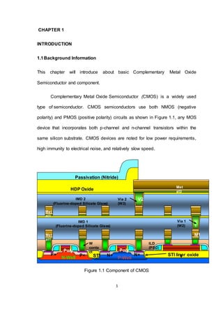
  • 1. 1 CHAPTER 1 INTRODUCTION 1.1Background Information This chapter will introduce about basic Complementary Metal Oxide Semiconductor and component. Complementary Metal Oxide Semiconductor (CMOS) is a widely used type of semiconductor. CMOS semiconductors use both NMOS (negative polarity) and PMOS (positive polarity) circuits as shown in Figure 1.1, any MOS device that incorporates both p-channel and n-channel transistors within the same silicon substrate. CMOS devices are noted for low power requirements, high immunity to electrical noise, and relatively slow speed. Figure 1.1 Component of CMOS IMD 1 (Fluorine-doped Silicate Glass) IMD 2 (Fluorine-doped Silicate Glass) HDP Oxide Passivation (Nitride) M3 M1 V 1 V2 Met al1 Met al2 STI STI liner oxide P-WellN-Well N+ N+P+ P+ Poly ILD (PSG) W conta ct Via 1 (W2) Met al3 Via 2 (W3) Poly
  • 2. 2 NMOS is an n-channel MOS transistor; in an NMOS device the channel is negative during conduction and PMOS is P-channel MOS transistor where the active carriers are holes flowing between p-type source and drain regions in an electrostatically formed p-channel in an n-type silicon substrate. The channel, the source, and the drain are made of a p-type semiconductor material. Photolithography is a process by which a mask pattern is transferred to a wafer, usually using a "stepper." Photo system made up of 2 components (track and stepper) to transfer a pattern in resist from a reticle (mask) onto the wafer. Photoresist is light-sensitive organic polymer that is exposed by the photolithography process, and then developed to produce a pattern which identifies some areas of the film to be etched. Etch the removal of unwanted material, by the se of acid (wet etch) or ionic bombardment (dry etch) to create a physical feature on a wafer surface, also a process for removing material in a specified area through a chemical reaction. Plasma Energy (Etching) is makes ions and free radicals. Ion bombardment damages (weak) the surface and gases from plasma chamber produces free radicals that react with the damaged surface and the gases leave the surface with atoms from the substrate. Chemical Mechanical Planarization (CMP) is a process that uses an abrasive, corrosive slurry to physically grind the microscopic topographic features on a partly processed wafer flat (planarization) so that subsequent processes can begin from a flat surface
  • 3. 3 Shallow Trench Isolation (STI) isolates each transistor from its adjacent transistor in order to prevent current leakage. Traditionally this isolation was accomplished with a LOCOS (localized oxidation of silicon) field oxide process. Polycrystalline silicon (Poly); extensively used as conductor or gate materials in a highly doped state. Poly films are typically deposited using high- temperature CVD technology. Contact is the portion of a microchip that is between the copper or aluminum interconnect and the transistor. This area is often filled with tungsten (W). Vias are holes through dielectric layers, opened by etching. Metal will be deposited in the via to form a plug and create an interconnect between two metal lines Interlayer Dielectric (ILD) Films used between metal layers of an IC for insulation. Insulator is nonconductive dielectric films used to isolate electrically active areas of the device or chip from one another. Some commonly used insulators are silicon dioxide, silicon nitride, boro-phospho-silicate glass (BPSG), and phospho-silicate glass (PSG) Metallization is the deposition of a layer of high-conductivity metal (such as aluminum) used to interconnect devices on a chip by CVD or PVD. Metals typically used include aluminum, tungsten and copper, etc. Interconnect is the wiring in an integrated circuit that connects the transistors to one another such as Metal 1, Metal 2 and beyond. Deposition of metal layer is addition of increases mechanical strength of metal. Chemical Vapor Deposition (CVD) is a process for depositing thin films from a chemical reaction
  • 4. 4 of a vapor or gas. Physical Vapor Deposition (PVD) also called sputtering is a process technology in which molecules of conducting material (aluminum, titanium nitride, etc.) are "sputtered" from a target of pure material, and then deposited on the wafer to create the conducting circuitry within the chip. Ion Implantation is a process technology in which ions of dopant chemicals (boron, arsenic, etc.) are accelerated in intense electrical fields to penetrate the surface of a wafer, thus changing the electrical characteristics of the material. Intermetal Dielectric (IMD) is Insulating films used between adjacent metal lines; typically silicon dioxide (SiO2). Dielectric Film is a non-conducting film in integrated circuits usually Si02 (Silicon Dioxide). High Density Plasma (HDP) is a plasma featuring high concentration of free electrons, and hence, high concentration of ions. Passivation is the final layer in a semiconductor device that forms a hermetic seal over the circuit elements. Plasma nitride and silicon dioxide are the materials primarily used for passivation. [1] As current technology advance by shrinking the minimum critical dimension to 20 nm and below, combined with the growing complexity of design, the traditional physical failure analysis method faces serious challenges due to the increase in non-visible defect and limited resolution. Latchup is formed by the parasitic path between VDD and VSS. This parasitic path is inherent in the bulk CMOS ICs. When the path is triggered on to conduct a huge current from VDD to VSS, the chip is often burned out. In order to find out the failure spots, some failure analysis (FA) procedures, including fault isolate step by Electrical
  • 5. 5 Characterizations and Scanning Optical Microscope (SOM), then inspection step by Delayering process of removal thin layers of metal or insulators onto a wafer during the wafer fabrication process using deposition and oxidation techniques observation by Optical Microscope and Scanning Electron Microscope (SEM) and confirming defect by Focused Ion Beam (FIB) and Energy Dispersive X-ray microanalysis (EDX) were applied to find out the root cause of defective device. Figure 1.2 CMOS Circuits in Silicon Wafer IMD 1 (Fluorine-doped Silicate Glass ) IMD 2 (Fluorine-doped Silicate Glass ) HDP Oxide Nitride M3 Met al1 Met al2 STI Local Oxidation of Silicone (LOCOS) N-WellP-Well Gate Ga te Via 1 Met al3 Via 2 So ur ce DrainSo ur ce Drain VddVss OUT IN Passivation
  • 6. 6 Figure 1.3 CMOS Circuit in Model Chart 1.2Problem Statement With the increasing complexity of process technology, devices features are now down to the deep sub-micron range and the number of metal has increased as many as 9 layers. At the same time failure analysis has become significantly more difficult, especially the fault localization. Many localization tool such as Light Induced Voltage Alteration (LIVA), Liquid Crystal (LC), Thermal Induced Voltage Alteration (TIVA), See beck Effect Imaging (SEI), Optical Beam Induced Resistance Change (OBIRCH), Scanning laser Optical Microscope (SOM) are not precise enough by themselves to pin point defect. However combining these techniques with layout tracing and Passive Voltage Contrast (PVC) can greatly improve the accuracy of defect isolation and increase failure analysis (FA) hit rate. Passive Voltage Contrast (PVC) in Scanning Electron Microscope (SEM) or Focused Ion Beam (FIB) is well known technique to identify leaky poly and open nodes in CMOS. GateGate Sour ce Sour ce Drain DrainVss OUT Vdd IN PMOSNMOS
  • 7. 7 1.3 Objectives of the project The main objective of this project is to perform failure analysis on defective failure in CMOS by:-  Identify defective CMOS using Electrical Curve tracer  Determine the defect location using fault isolate technique, Scanning laser Optical Microscope (SOM)  Identify the defect precise location of the defect and it symptoms by Passive Voltage Contrast (PVC) technique using Scanning Electron Microscope (SEM)  Reconfirm the root cause of defect using Focused Ion Beam (FIB) and Energy Dispersive X-ray microanalysis (EDX). Identifying the type of defect in the CMOS based on it symptom and determine the root cause of the defect the CMOS. So from the root cause of defective sample, related process causes the defect will be determine, precaution step will more alert on the step to prevent the defect repeat and the best suggestion for improvement the step related will given to solve the problem.
  • 8. 8 CHAPTER 2 LITERATURE REVIEW The resistivity of a film refers to its ability to conduct an electrical current. Resistivity is the opposite of conductivity. Bulk resistivity is a measurement of a material property. The bulk resistivity of a material will remain the same regardless of its thickness. Different materials have different bulk resistivity. Metals have low bulk resistivity. Semiconductors have high bulk resistivity. Insulators have infinite resistivity. They do not conduct electrical current shown in Table 1. Sheet Resistance is a measurement of how well a sheet of thin film conducts electricity. The sheet resistance will decrease as the thickness increases, in the same way that a larger fuse will allow more current to flow before blowing than a small fuse will. Sheet resistance and bulk resistivity are related by thickness [3] Material Bulk Resistivity Aluminum 2.7 Titanium 42 Tungsten 10.4 Cobalt 6.2 Titanium Nitride 600 Pure Silicon > 1,000,000 p-Type Silicon 4 Table 1 Bulk Resistivity of Material
  • 9. 9 SiO2 (Silicon Dioxide) is the silicon/oxygen film most often used for dielectric applications; can be deposited via silane or Tetraethylorthosilicate (TEOS); often called "oxide." Fluorine-doped Silicate Glass (FSG) is a reduced dielectric constant (k=approximately 3.5) material made by doping SiO2 with fluorine. Low K is a dielectric material having relatively greater insulating ability than silicon dioxide (SiO2), usually with a k<3.5. [4] Low-K Via Poisoning happens when the Low-K is on top of the metal and a via hole is opened through it.The exposed Low-K film out gasses during TiN and W deposition deterring via fill as shown in Figure 2.1and Figure 2.2 [5] Figure 1.1 Good Via Figure 2.2 Poisoned Via The ability of new layers to evenly cover the steps already formed on the wafer is called step coverage. A tapered profile allows new layers to evenly cover the surface. As devices become smaller, the contacts must become less tapered or they will overlap. They also become more narrow and deeper. Sputtering is directional. The sputtered atoms stick on the site where they first land. This gives excess deposition on the edges. Sputtering gives poor step coverage. CVD is a gaseous process. A gas expands to fill a volume. Reactive
  • 10. 10 species sample many sites. They only deposit an atom on stable site.CVD gives good step coverage. [5] PVC (Passive Voltage Contrast) fault isolation method by using a SEM (Scanning Electron Microscope) has been widely used for isolating the defective mc (metal contact) in the CMOS logic SRAM bit cell array. The low power (LP) processed SRAM cells are easy to charging under PVC test and it helps isolating defective contacts in the cell. However, some device such as a high speed (HS) SRAM cell is hard to charging inPVC test by unknown reason. It makes difficulties for isolating defective contacts in the SRAM cell array. In this paper, our group analyzed the electrical current of each contact in SRAM cell using a nanoprobing technique and correlated it with PVC charged contact images, respectively.[6] Contact structures were very difficult to verify to be a high resistance open issue or a bridge/leakage short issue. FIB passive voltage contrast was very successfully implemented in 2 Mb SRAM debug to differentiate the two failure mechanisms, high via and/or contact resistance versus substrate defect-induced junction leakage. It was demonstrated in four different cases that passive voltage contrast was used to reveal and locate the specific failure site and followed with pinpoint diagnosis of the abnormality by TEM. It was also known that these defects were invisible to optical microscopy and SEM. The 2Mb SRAM process was a 0.25 μm, three-metal single-poly, 8-inch technology. Shallow trench isolation (STI), self-aligned TiSi2 silicide (salicide), and triple stacked W-plug processes were integrated in the manufacturing process. The failure mode and failure location were firstly identified by a MOSAID tester. Layer-by-layer deprocessing and top-view SEM examination were used for structural inspection
  • 11. 11 at the Failure site prior to FIB imaging. As soon as the fault was isolated by a passive voltage contrast comparison study, precision TEM analyses were utilized as the major tool for structural inspection in both plan-view and cross-section The common Passive Voltage Contrast localization method in Focused Ion Beams and Scanning Electron Microscopes can be used for failure localization issues. These methods became widely accepted in the semiconductor failure analysis community. Nearly all labs make use of it. The Active Voltage Contrast method works with additional external voltages applied inside the chamber to certain structures at the sample surface and offers even more localization possibilities. A comprehensive overview over all phenomena related to Voltage Contrast generation is given and the multiple advantages, possibilities and limits of VC failure localization. Many process defects and errors can produce failing vias ,via voiding, particulates, and via pushup. Via failure requires both resistive interconnection formation and performance demands resulting in a functional failure [8] Figure 2.3 (Left) Floating Via and (Right) Missing Via
  • 12. 12 Figure 2.4 Directions of applied electric field and resulting carrier drift velocity and drift current density in (a) an n-type semiconductor and (b) a p-type semiconductor The two basic processes which cause electrons and holes to move in a semiconductor are: (a) drift, which is the movement caused by electric fields, and (b) diffusion, which is the flow caused by variations in the concentration, that is, concentration gradients. Such gradients can be caused by a non-homogeneous doping distribution, or by the injection of a quantity of electrons or holes into a region. Consider an ntype semiconductor with a large number of free electrons (Figure 2.4). An electric field E applied in one direction produces a force on the electrons in the opposite direction, because of the electrons’ negative charge. The electrons acquire a drift velocity vdn (in cm/s) where μn is a constant called the electron mobility and has units of cm2/V–s. For low-doped silicon, the value of μn is typically 1350 cm2/V–s. The mobility can be thought of as a parameter indicating how well an electron can move in a semiconductor. a b Ē Ē ē h+ JJ ˉˉ n p v v dn dpˉˉ n type p type
  • 13. 13 The negative sign in indicates that the electron drift velocity is opposite to that of the applied electric field as shown in Figure 2.4. The electron drift produces a drift current density Jn (A/cm2) given by where n is the electron concentration (#/cm3) and e, in this context, is the magnitude of the electronic charge. The conventional drift current is in the opposite direction from the flow of negative charge, which means that the drift 13 current in an n-type semiconductor is in the same direction as the applied electric field. Next consider a p-type semiconductor with a large number of holes. An electric field E applied in one direction produces a force on the holes in the same direction, because of the positive charge on the holes. The holes acquire a drift velocity vdp (in cm/s), μp is a constant called the hole mobility, and again has units of cm2/V– s. For low-doped silicon, the value of μp is typically 480 cm2/V– s, which is less than half the value of the electron mobility. The positive sign in equation indicates that the hole drift velocity is in the same direction as the applied electric field. The hole drift produces a drift current density Jp (A/cm2) given where p is the hole concentration (#/cm3) and e is again the magnitude of the electronic charge. The conventional drift current is in the same direction as the flow of positive charge, which means that the drift current in a p-type material is also in the same direction as the applied electric field. Since a semiconductor contains both electrons and holes, the total drift current density is the sum of the electron and hole components. The conductivity is related to the concentration of electrons and holes.
  • 14. 14 If the electric field is the result of applying a voltage to the semiconductor, then equation becomes a linear relationship between current and voltage and is one form of Ohm’s law. The conductivity can be changed from strongly n-type, n p, by donor impurity doping to strongly p-type, p n, by acceptor impurity doping. Being able to control the conductivity of a semiconductor by selective doping is what enables us to fabricate the variety of electronic devices that are available.[9]
  • 15. 15 CHAPTER 3 THEORY This chapter about theory operation of CMOS, theory fabrication in CMOS, theory failure analysis technique; Theory of Passive Voltage Contrast, theory of electrical characterization, theory of Scanning Optical Microscope (SOM), theory of Scanning Electron Microcope (SEM), theory of Focused Ion Beam (FIB) and theory of Energy Dispersive X-ray microanalysis (EDX) 3.1Theory of Device CMOS MOFSET (MOS Transistor) is a simple structure for a simple function and it divide to n- MOFSET and p-MOFSET. n-MOFSET are n+ Si consists a large number of electrons negative charge) and negligible number of holes (positive charge). The typical number of electrons ~ 1020 cm-3 and holes ~ 2 cm-3. p+ Si consists of holes (positive charge) and less number of electrons positive charge). Typical number of holes ~ 1017 cm-3 and electrons ~ 2.25X103 cm-3. Positive gate voltage attracts negative charged electrons to close the “switch” to ON State Figure 3.1 Basic Structure of n-MOFSET
  • 16. 16 p-MOFSETp+ Si consists a large number of holes (positive charge) and negligible number of electrons (negative charge). Typical # of holes ~ 1020 cm-3 and electrons ~ 2 cm-3. n Si consists of electrons (negative charge) and less number of holes (positive charge). Typical # of electrons ~ 1017 cm-3 and holes ~ 2.25X103 cm-3. Negative gate voltage attracts positive charged holes to close the “switch” to ON State Figure 3.2 Basic Structure of p-MOFSET 3.2 Theory of PVC (Passive Voltage Contrast) Passive Voltage Contrast techniques have identified structures at potential different from those expected. Passive Voltage Contrast is defined as contrast which arises from voltage differences induced by restoring the beam when various elements reach an equilibrium potential through self-charging. Contrast is generated by differences in secondary electron emission yields caused by difference in potential when imaging with a primary beam energy of 1keV, areas that are at positive potential appear dark in the images and those that are at ground appear dark. It has been possible by increasing the accelerating potential to observe a polarity change in the feature which was charging due to a crossover in the secondary electron emission efficiency.
  • 17. 17 Figure 3.3 Basic Structure of Passive Voltage Contrast Figure 3.4 (Left) Dark VC compare (Right) Normal VC Dark VC at Contact Normal VC at Contact
  • 18. 18 3.3 Theory of I-V Curve Characterization Figure 3.5 IV curve Diffusion is the process of particles distributing themselves from regions of high concentration to regions of low concentration. If this process is left unperturbed, there will eventually be a uniform distribution of particles. Diffusion does not need external forces to act upon a group of particles. The particles move about using only thermal motion. If we let the particles be carriers, so as they move around they take charge with them. The moving of charge will result in a current. We call this current due to diffusion. The difference between drift current and diffusion current is that drift current depends on the electric field applied: if there's no electric field, there's no drift current. Diffusion current occurs even though there isn't an electric field
  • 19. 19 applied to the semiconductor as shown on Figure3.5. It does not have E as one of its parameters. The constants it does depend on are Dp and Dn, and +q and - q, for holes and electrons respectively. The first constants are called the diffusion coefficients, a proportionality factor. We don't worry too much about these because they are constants. We do worry about the gradient of the concentration of p and/or n, though. But, since we are talking about a one dimensional situation when we are solving for current densities, we only worry about the gradient (or derivative) with respect to the x-plane. The other difference between drift current and diffusion current, is that the direction of the diffusion current depends on the change in the carrier concentrations, not the concentrations themselves. In the equation, the signs are reversed as we are used to seeing them. We usually assign a +q to holes and - q to electrons. In the case of diffusion current, they are reversed to be opposite of the derivative of the concentrations. This occurs because the carriers are diffusing from areas of high concentrations to areas of low concentrations. For example, if the derivative of p with respect to x is positive, then the concentration of holes is growing as you move towards the +x direction. Diffusion current will be the opposite of that, the holes will be diffusing in the -x direction to where there's a lower concentration of holes. If the derivative is negative, the opposite will occur. The concentration of holes is decreasing as you go from the - x to +x direction. Therefore, holes will diffuse to the +x direction where there's a lower concentration of holes. This is why the negative sign is needed in the equation for the hole diffusion current.
  • 20. 20 The same goes for electrons, but in this case, the signs cancel for a positive derivative because the electrons, carrying -q, diffuse to the -x direction where there's less electrons. The sign remains if the derivative is negative, because electrons will be diffusing to the +x direction carrying a -q charge. For these reasons it's not included in the equation for the electron diffusion current. Both drift current and diffusion current make up the total current in a semiconductor. They may not be occurring at the same time, but the equation is still valid. Under equilibrium conditions, the current density should be zero because there shouldn't be any drastic changes occurring, like applying an electric field or changing the carrier concentrations by a large margin. Even so, if the doping is not completely uniform, there will be a change in concentration is some places in the semiconductor, resulting in a gradient. This gradient can in turn give rise to an electric field, which in turn can give rise to non-zero current densities. 3.4 Theory of Scanning Optical Microscope (SOM) The reflected laser beam intensity depends on the reflectivity of the surface. This is being used for high resolution imaging purpose. For the absorbed laser energy, it will be either generate temperature change or electron hole generation. Any change in the device parameters due to laser induced change will affect the power change in the device. Device parameters change can also be detected using the tester. These are the phenomena that SEMICAPS SOM are detecting. Termed a scanning optical microscope (SOM) in the electronics world, the SOM was first developed for biological applications in the form of a confocal
  • 21. 21 microscope. The basic confocal concept is straightforward (Fig. 1). A high- brightness point source (typically a laser) is focused onto the target, and the reflected light is then reimaged onto a point detector. Confocal literally means twice focused. An image of the target is formed by scanning the focused spot over the target and collecting the detected light intensity as a function of scan position. A computer is used to produce a recognizable image from the collected data. Non-confocal SOMs exist, but this article considers only this basic configuration. Clearly, a SOM is mechanically more complex than a digital camera, but it offers certain advantages that make it very attractive in the biological world: Improved transverse resolution of ~30%, ability to obtain depth slices—specifically, out-offocus components appear black ,the source and detector can respond at different wavelengths, allowing configurations for fluorescence microscopy and other spectroscopic techniques. The second property is of particular importance in biology because it facilitates focusing inside of a sample without the interference of intervening objects, for example, examining the internal components of a cell. Spectroscopic techniques have opened a wide range of applications in microbiological imaging The improved imaging properties of a SOM are of some value in the semiconductor world. However, the more important use of a SOM resides in its ability to direct a small spot of light into an integrated circuit and thereby inject a localized signal. The photons in the light spot interact with the circuit in one of two ways: Generation of photocarriers in the semiconductor material. Generation of heat in all components The first interaction occurs only if the light source has
  • 22. 22 photon energy above the semiconductor bandgap. Photon energy below the semiconductor bandgap allows only heat generation. The bandgap dependence of the two generation methods is shown on the graph of silicon optical absorption in. Both photocarrier and heat generation affect the current-voltage (I-V) characteristics of the circuit area being illuminated through the photovoltaic, photoconductive, thermal electric (thermocouple), and thermal-conductive effects. Each of these four effects has a slightly different effect on the I-V curve. The photovoltaic effect acts as a current generator, shifting the curve along the current axis. The photo-conductive effect shifts the device resistance—always lower. The thermal electric effect acts a voltage generator, shifting the curve along the voltage axis. The thermal-conductive effect shifts the device resistance up or down depending on the material. A major difference between the photocarrier and heating effects is that the former affects only the silicon, whereas the latter affects all the circuit elements, for example, lines and vias. Photocarrier effects are also orders of magnitude larger than thermal effects, and they dominate at the shorter laser wavelength (1.064 μm). Various means are used to sense changes in the I-V characteristics produced by a SOM. Each has its own acronym, for example, optical beam induced current (OBIC), light-induced voltage alteration (LIVA), thermally induced voltage alteration (TIVA), optical beam induced resistance change (OBIRCH), externally induced voltage alteration (XIVA), laser-assisted device alteration (LADA), soft defect localization (SDL), and so on, depending on the sensing technique used and the type of defect being explored. The generalized term, laser signal injection microscopy (LSIM), was coined to cover the broad spectrum of FA techniques available using a SOM tool.
  • 23. 23 Figure 3.6 SOM Block Layout Figure 3.7 SOM Optical Layout
  • 24. 24 3.5 Theory of Scanning Electron Microscope (SEM) Regular microscopes focus visible light onto the sample and return the images to the human eye. There's a limit however to the amount of magnification that can obtain no matter how good the equipment. This is because normal light has a wavelength that allows us to obtain a maximum magnification of only around 2000x. Moreover, the images lack the proper depth since the focal length has to be adjusted accordingly. Scanning electron microscopy uses the secondary electrons generated by bombarding a sample with an electron beam to generate an image. This secondary electron image can be used with a certain degree of interpretation as an implied topographical shot - things like surface roughness and uniformity can be qualitatively examined. Additionally, a secondary electron image will often show differences in the conductivities of materials, due to the charging effects observed as the beam scans across the surface of the part; this can be useful for identifying contaminants on the surface of a device. In addition to these techniques, there are other applications for the SEM that can provide contrast based on the materials present on a device. When backscattered electrons are collected instead of secondary electrons, the scanning electron microscope can provide an entirely different view of the same sample. When generating a backscatter image, contrast is determined elementally; the further apart two elements appear on the periodic table, the higher the contrast will be between them on the SEM image. Using backscatter images to identify elemental changes can be a useful precursor for more in-depth chemical analysis like energy dispersive spectroscopy; being able
  • 25. 25 to visually see material changes can greatly influence the sites chosen for a more in-depth look. Scanning electron microscope operating modes the only techniques available for examining devices or materials. Changing accelerating voltages and currents, applying outside stimuli (like voltage pulses), or examining a material under different levels of vacuum can all create vastly different SEM images. Being able to generate an image is only half of the battle, however; it is still crucial to know which images are the most valuable, and how to select a given imaging mode based on the needs of the analysis. Using electron microscopy however, it's possible to generate images that are a thousand times more detailed than those delivered by an optical microscope of electrons as particles, they can just as easily behave exactly like waves and as with all waves, they have a wavelength which is inversely proportional to their momentum which in turn is under our control depending on how much energy we pump into the electron beam. The images generated are monochromatic since no color information is passed. But a tremendous depth is generated which makes electron scanning microscopy uniquely suited for failure analysis. A side effect of the electron microscopy service is that the beam of electrons can also end up generating x-rays by knocking out an electron in the ground state of some atoms. This leaves a "hole" which a higher shell electron hurries to fill up thus discharging the "characteristic x-rays" which provides useful information about the elemental structure of the sample. It overlaps with x-ray imaging techniques.
  • 26. 26 Semi conductors are particularly well suited to failure analysis using scanning electron microscopy due to the unique mechanism by which they conducts charge carriers. It eases the preparation of the sample which usually requires a coating of some conductor like gold or platinum. In fact, in no other field is electron microscopy used so widely as it is in failure analysis. 3.6 Theory of Focused Ion Beam (FIB) Focused ion beam (FIB) systems have been produced commercially for more than twenty years, primarily for large semiconductor manufacturers. FIB systems operate in a similar fashion to a scanning electron microscope (SEM) except, rather than a beam of electrons, FIB systems use a finely focused beam of gallium ions that can be operated at low beam currents for imaging or high beam currents for site specific sputtering or milling. As the diagram on the right shows, the gallium (Ga+) primary ion beam hits the sample surface and sputters a small amount of material, which leaves the surface as either secondary ions (i+ or i-) or neutral atoms (n0). The primary beam also produces secondary electrons (e-). As the primary beam rasters on the sample surface, the signal from the sputtered ions or secondary electrons is collected to form an image. At low primary beam currents, very little material is sputtered. Modern FIB systems, such as our newest Zeiss system, can achieve under 1 nm imaging
  • 27. 27 resolution. At higher primary currents, a great deal of material can be removed by sputtering, allowing precision milling of the specimen down to a submicron scale. If the sample is non-conductive, a low energy electron flood gun can be used to provide charge neutralization. In this manner, by imaging with positive secondary ions using the positive primary ion beam, even highly insulated samples can be imaged and milled without a conducting surface coating, as would be required in a SEM. In addition to primary ion beam sputtering, our system permits local "flooding" of the specimen with a variety of gases. These gases can interact with the primary gallium beam to provide selective gas assisted chemical etching, or selective deposition of (either) conductive or insulating material, enabled by the primary ion beam decomposing the deposition gas. Figure 3.8 FIB operation Until recently, the overwhelming usage of FIB has been in the semiconductor industry. Such applications as defect analysis, circuit modification,
  • 28. 28 mask repair and transmission electron microscope sample preparation of site specific locations on integrated circuits have become commonplace procedures. The latest FIB systems have high resolution imaging capability; this capability coupled with in situ sectioning has eliminated the need, in many cases, to examine FIB sectioned specimens in the SEM. As well as offering a full suite of semiconductor FIB services such as device modification, probe pad formation and TEM specimen preparation, Fibics Incorporated has pioneered a number of applications of FIB in materials science. These applications extend from site specific TEM specimen preparation of "difficult" materials, such as thin coatings of TiN on high speed steel through to applications in measurement of crack growth and aspect ratio during stress corrosion cracking, deformation of metal matrix composites, adhesion of polymer coatings, et cetera FIB is a charged particle beam with a much greater mass than the charged particles (electron) used in FEB (Focused Electron Beam). As shown in several other applications and tutorials here, this greater mass allows the FIB to sputter away matter as the beam hits the surface of the targeted material. It is possible to reverse this process if a gas is introduced in the vicinity of the impact point: this is called FIB induced deposition (FID). The gas is introduced by a nozzle which is positioned a few hundreds of microns above the area of interest. The gas is then adsorbed on the surface of the material. When the FIB beam hits the surface, secondary electrons with energy ranging from a few eV to a few hundreds of eV are generated. These
  • 29. 29 secondary electrons will break chemical bounds of the adsorbed gas molecules which will separate into different components: some of which remains volatile, others will form a deposition on the surface. If the FIB beam sits too long on the same location, the freshly deposited material will be sputtered away. The gas needs to be replenished in order to maintain a net positive yield. For this reason, once the beam has dissociated much of the adsorbed gas, it moves to another location before coming back to the same point. The time between two subsequent "visits" is called the refresh time. Once additional molecules have been adsorbed on the surface, the beam can revisit the same point and then increase the deposition thickness. A tight beam control (refresh time, beam spacing, focus, dwell time) is critical to a successful FID since the precursor gas can easily be depleted and then result in material sputtering instead of deposition. Different precursor gases create different depositions. Common deposition materials include Tungsten, Platinum, Carbon and Insulator. 3.7 Theory of Energy Dispersive X-ray microanalysis (EDX) Electron beam microanalysis is a powerful, non-destructive, analytical technique, capable of performing elemental analysis of micro-volumes, typically of the order of a few cubic micrometers. Although there are several other microanalytical techniques, each with their own specific advantages, none are better than X-ray microanalysis for routine chemical analysis of small volumes. When X-ray analysis is combined with electron imaging techniques, one has a powerful tool
  • 30. 30 for understanding the composition and structure of materials. Energy Dispersive X-ray microanalysis or EDX is an electron beam induced X-ray spectrochemical technique which allows the determination of the local chemical composition of a solid sample by means of an 'in situ', non-destructive, analysis on a microscopic scale. It is a powerful microanalytical tool compatible with both scanning and transmission electron microscopes. In both types of microscope, the electron beam is focused on an area of interest of the specimen. As a result of the interactions between the impinging electrons and the target atoms, X-rays are emitted which are characteristic in energy for the constituent chemical elements. A histogram of the X-ray intensities versus their energy, called an X-ray spectrum, enables not only the identification but also the quantification of the chemical elements present in the specimen. The quantitative accuracy is comparable to macroscopic physical techniques of elemental analysis. The spot size controls the physical size of the beam scanning on the specimen; spot 1 is the smallest and spot 7 is the largest. Changing from spot 1 to spot 2 increases the physical size of the spot by a factor 2 and also increases the number of electrons (ie beam current) by a factor of 4. This rule applies for every increase in spot size, ie from 2 to 3, from 3 to 4 etc. The accelerating voltage, or kV, controls the speed at which electrons hit the specimen and also therefore the depth of penetration of the beam into the specimen.
  • 31. 31 A higher kV gives better resolution so long as the specimen is conducting electrons sufficiently to prevent charging effects. The primary beam kV must be higher in energy than the critical excitation energy (Ec) of the element to be excited, otherwise the atom will not be excited. As the energy of the electron exceeds Ec, more efficient excitation of the element occurs as we have more ‘overvoltage’. The peak to background of an element does not change after the electron has an energy of 2Ec. Typically, the overvoltage used should be at least 2 times for the highest energy line and no more than 10-20 times for the lowest energy line. For example, Fe K is at 6.4KeV, which means that at 6.4kV primary beam energy the Fe K peak will start to appear on the spectrum. It will increase in height against the background up until 2Ec (2 x 6.4 = 12.8kV). Anything above 12.8kV would begin to degrade spatial resolution, as shown in figure 2. With Oxygen the O K is 0.52 KeV, so a good kV for Oxygen would therefore be between 5 and 10kV. If looking for both of these elements then 10kV would be a compromise. In view of the small volume involved, namely the beam-specimen interaction volume, the EDX technique is particularly suited for determining the local chemical composition of inhomogeneous specimens, chemical composition of very small quantities of material or small particles of matter, spatial concentration distribution or gradients of the constituent chemical elements in an inhomogeneous specimen, either along a line (line-scan) or over an area (X-ray
  • 32. 32 mapping) and chemical composition of thin films deposited on arbitrary substrate materials Some relevant characteristics of the EDX technique are range of chemical elements as all elements of the periodic system from beryllium onwards, minimum detectable mass fraction from 0.2 wt% to 1 wt% (weight percentage), the relative accuracy of quantitative results lies between 2 and 20 % depending on the complexity of the correction method employed and whether or not the analysis is based on known chemical standards, time of analysis well below 1 minutes for up to 16 elements by PC controlled data acquisition and on-line data reduction, spatial resolution depends on the mean atomic number and density of the specimen and also on the primary beam energy; 0.2 - 10 micron Scanning Electron Microscope (SEM). Backscattered electron images in the SEM display compositional contrast that results from different atomic number elements and their distributionEDX allows one to identify what those particular elements are and their relative proportions (Atomic % for example). Initial EDX analysis usually involves the generation of an X-ray spectrum from the entire scan area of the SEM. Below is a secondary electron image of a polished geological specimen and the corresponding X-ray spectra that was generated from the entire scan area. The Y-axis shows the counts (number of Xrays received and processed by the detector) and the X-axis shows the energy level of those counts For a reliable analytical result, the sample preparation must satisfy certain requirements as the specimen must be flat and smooth, especially for quantitative analysis; usually specimens are polished, EDX enables analysis of rough
  • 33. 33 specimens; however, application is limited to qualitative and semi-quantitative determinations, The specimen must be electrically and thermally conducting; if necessary, the specimens are coated by means of vacuum evaporation or sputtering with a thin layer of carbon (C) or gold (Au). These are powerful and useful forms of elemental analysis. However, as with any technique, there are constraints with which should be familiar. Below is a list [1] of some of those, Energy resolution: 130 eV (Full Width Half Max) at Mn Kα, Limit of detection: 1000 – 3000 ppm; >10% wt% ,elements identified: elements heavier than Beryllium, spatial resolution: Low atomic number (Z): 1-5 um3 ; High Z: 0.2 – 1 um3, precision (the closeness of agreement between randomly selected individual measurements): approaching ±0.1%, accuracy (the closeness of agreement between an observed value and an accepted reference value): (95% analysis). ±1% for polished bulk target, pure standards on site ±2% for polished bulk target, standards collected on another SEM and then corrected for the geometry and settings of the present microscope . ±5% for particles and rough surfaces “without standards” Obviously all of these constraints are important to understand; however, spatial resolution of the signal is often surprising to newcomers. The units of spatial resolution are microns -- not nanometers. This is due to the fact that X-rays are generated from very deep in the interaction volume. Also, it is common to use intermediate (15—20 keV) accelerating voltages to ensure the peaks one wishes to record. The size of the interaction volume icreases with accelerating voltage. EDS is certainly not a surface analysis technique. It doesn’t take much magnification in the SEM to reach the point where
  • 34. 34 the pixel size on the specimen approaches this dimension. You may want to consider Wavelength Dispersive Spectroscopy if you are in need of better: limits of detection (30—300 ppm; 1% wt%); performance for light elements; energy resolution (10 eV [FWHM] at Mn Kα); precision and accuracy. Energy Dispersive X-ray microanalysis (EDX analysis) can summarise as large spot size gives faster results as it gives higher CPS, change in spot size has little effect on change in spatial resolution, increasing kV allows detection of higher atomic number elements, higher kV results in larger interaction volume and interaction volume is large for EDX analysis (2-5m) As a general rule for materials containing light elements, 5kV is a good choice and for many metals and alloys, 20-30kV is a good choice. Heavier elements may be analyzed using L or M lines and when performing EDX on an unknown sample, it may be best to perform analysis at two kVs, eg 5 and 20, to confirm the presence of certain elements. Summary of theory Base on theory of device flow and basic operation of CMOS, theory of fabrication show critical process step will occur defect on CMOS and theory of failure analysis technique help in find out root cause of defect on CMOS such as electrical characterization using IV tracer, Scanning Optical Microscope (SOM) for detect defect location, Scanning Electron Microscope (SEM) for inspection and confirmation type of defect by Focused Ion Beam (FIB) and Energy Dispersive X-ray microanalysis (EDX)
  • 35. 35 CHAPTER 4 METHODOLOGY This chapter about process flow for inspect 5 devices with 46 sample using failure analysis technique in CMOS to find out the root cause of defect base on it symptom 4.1 Process Flow Figure 4.0 Process Flow Defective Sample Fault Isolate (localization) • Electrical Characterizations • Scanning Optical Microscope (SOM) Inspection/Observation • Delayering (Parallel Lapping) • Optical Microscope (OM)(Pre Inspection) • Passive Voltage Contrast (PVC) • Scanning Electron Microscope (SEM) Confirmation • Focused Ion Beam (FIB) • Energy Dispersive X-ray microanalysis (EDX)
  • 36. 36 4.2 Apparatus 4.2.0 Defective samples 4.2.1 IV tracer Agilent 4156B 4.2.2 Semicaps SOM 4000 4.2.3 Precision Polisher Allied 4.2.4 Optical Microscope 4.2.5 Field Emission Scanning Electron (Zeiss Ultra 55) 4.2.6 Focused Ion Beam (FEI Dual Beam 835) 4.3 Fault Isolation 4.3.1 Electrical Characterization using IV tracer Figure 4.1 IV Tracer Agilent 4156B 1) The Sample placed on the stage 2) The Pin probe at pad Vdd vs. Vss as shown in Figure 4.2 3) The Parameter current, voltage, compliance and others set up 4) Run sample 5) Monitor and save the data of leakage current as shown in Figure 4.3 and Figure 4.4
  • 37. 37 Figure 4.2 Pad Probe Figure 4.3 IV Tracer Show result in good condition
  • 38. 38 Figure 4.4 IV Tracer Show result in bad condition (high leakage)
  • 39. 39 4.3.2 Scanning Optical Electron (SOM) Figure 4.5 Semicap SOM4000 1) The sample place on stage (make sure nothing blocking the sample at back) 2) Probe Pin at pad Vdd and Vss as shown in Figure 4.2 3) lens set at 0.5x 4) Focus the image 5) Run sample 6) Set the back ground with voltage flow off 7) Then set repeat for flow the voltage 8) Flip the image and observe hot spot 9) Zoom in location hot spot until UHR50x 10)For detail and clear image can use laser imaging Sample Pad Bias Voltage Contrast (VBA) InGaAs Monitor Controller
  • 40. 40 4.4 Pre Inspection 4.4.1 Precision Polisher Figure 4.6 sample on finger 1) The pad surface cleaned with DI water and rubber pad 2) Put slurry on the pad to improve delayering process due to slurry grain size is 0.05µ 3) Rotation speed set at 180rpm for parallel lapping and around 100rpm for cross section lapping. 4) Sample put on the pad and push the sample gentle 5) Press Start button 6) Sample inspect frequently at OM to prevent over lapping. Polisher
  • 41. 41 4.4.2 Optical Microscope Figure 4.7 sample under microscope 1) Clean the sample using organic soap and DI water. 2) Blow sample with air gun. 3) Put the sample under lens and observe any abnormality at the layer. 4) Change lens magnification for close up or zoom out. Sample Optical Microscope
  • 42. 42 4.5 Inspection 4.5.1 Scanning Electron Microscope (SEM) Figure 4.8 Scanning Electron Microscope 4.5.1.1 Loading sample 1) Open the airlock door and loading the sample. 2) Close door and press “ Store “ button, wait until the [ store ] LED and [ rod retracted ] LED switch on 3) Press “Exchange “button on hard panel controller. 4) Wait the indoor of airlock open, then loading the sample inside the vacuum chamber. 5) After that, pull out the rod completely and press “Store “button. 6) Then click “Resume Exchange “on airlock panel on monitor or press “Resume “button on hard panel controller.
  • 43. 43 4.5.1.2 Inspect Sample 1. Verified eccentric height 3.5mm 2. Focusing the sample image with rotate knob clock wise (in focus) or anti clockwise (out focus). 3. Don’t focus at your location during to avoid sample burn cause of ion beam. 4. Can focus at particle or any metal not your location for adjust X-Y stigma. 5. Go to location and adjust knob Brightness and Contrast to get good image. 6. Passive Voltage Contras (PVC) inspection, use power around 0.7kV. 7. PVC inspection can observe image on surface. 8. Brightness and Contrast percentage important to get accurate VC image. 9. High Current Voltage Inspection, use power around 20kV. 10.Can inspect layer below the surface by focusing knob. 11.Zoom the image magnification base on the profile sample, low magnification 3kX – 5kX and high magnification 10kX – 20kX. 12.Save the image. 4.5.1.3 Unloading sample 1) After finish the job and taken the SEM image, first OFF EHT, then press “Exchange “button on hard panel controller. 2) Wait the indoor of airlock open, then push in the rod for taking out the sample from vacuum chamber completely. 3) Press “Store “button. 4) Press “Vent “button, and then take out the sample.
  • 44. 44 5) If continues to use the machine, follow the step as below: a) First, exchange the sample. b) Press ‘store “button. c) Press “transfer “button, wait until indoor airlock open. d) Push in the sample to vacuum chamber, and then take out the rod completely. e) Press ‘store ‘button, then press “resume “button on hard panel controller. 6) If not use the machine, take out the sample, press “ store “, then press “ Resume “ button on hard panel controller.
  • 45. 45 4.5.2 Focused Ion Beam (FIB) Figure 4.9 Focused Ion Beam 1) The sample place on stage with cover half sample with copper tape to prevent charging image. 2) Load sample into load/lock and waiting system pump down. 3) Find the location by click at the stage map. 4) Focus image at low magnification. 5) Align sample to horizontal 6) Get one point as reference to tilt the sample. 7) Adjust eccentric (Tilt sample to 52⁰) 8) Go to location, Zoom, Focused and align sample 9) Cap the location using platinum ±0.2µ to prevents structure from collapse 10)Made box near to location for monitoring 11)Perform cutting using ion beam 12)Tuning image at electron beam until clear 13)Save the image. 14)Unload the sample.
  • 46. 46 4.5.3 Energy Dispersive X-ray microanalysis (EDX) 1 Spot size change in spatial resolution 2 Increasing kV allows detection of higher atomic number elements 3 Higher kV results in larger interaction volume 4 Interaction volume is large for EDX analysis (2-5m) 5 The EDX Mode with the TLD or BSE detector 6 Spatial resolution depends on the mean atomic number and density of the specimen and also on the primary beam energy; 0.2 - 10 micron in a SEM. 4.6 Summary In analytical lab, even the most sophisticated and accurate equipment will provide incorrect result if samples have not appropriately collected and handled, if the equipment has not been use correctly or if analytical protocol have not been followed. Two concerns associated with measurements of element are unrecognized contamination and inadequate quality assurance. Contamination can occur during sample preparation, collection, sample storage and transport. Specific protocols are available for the different analytical methods. These must be strictly adhered to contamination risks can be significantly reduced by the application of adequate QA measures.
  • 47. 47 CHAPTER 5 RESULT and DISCUSSION 5.1 Device A 5.1.1 Result Electrical Characterization Biasing condition:- VCCDIG = GROUND VSSDIG = sweep from –1.4V to 1.4V Figure 5.0 IV curve showed Bad die leakage higher than Good die -0.15 -0.1 -0.05 0 0.05 -2 -1 0 1 2 CURRENT(A) VOLTAGE (V) DCCDIG vs VSSDIG GOOD S2 S3 S4 S5 S6 S7 S8 S9 S10
  • 48. 48 5.1.2 Result SOM Figure 5.1 Hot Spot images in 5x and 20x magnification 5.1.3 SEM HKV/PVC RESULT Figure 5.2 SEM PVC image showed dark VC at Metal 1 and SEM HKV image showed abnormalities at contact location 5x 20x
  • 49. 49 5.1.4 Result FIB cut at dark VC location Figure 5.3 FIB cut found unfilled contact
  • 50. 50 5.2 Result Device B 5.2.1 Result Electrical Characterization Biasing condition:- VSSDIG4 = GROUND VCCDIG = sweep from –1.5V to 1.5V Figure 5.4 IV showed Bad die A5 high leakage at drift current compare with Good die (A10) 5.2.2 Result SOM Figure 5.5 Common Hot Spot observe at all sample -0.12 -0.1 -0.08 -0.06 -0.04 -0.02 0 0.02 -2 -1.5 -1 -0.5 0 0.5 1 1.5 2 CURRENT(A) VOLTAGE (V) VCC vs VSS A3 A4 A5 A6 A7 A8 A9 A10
  • 51. 51 5.2.3 SEM HKV/PVC RESULT Figure 5.6 SEM PVC/HKV images showed no abnormalities at Metal 1 layer Figure 5.7 Contact layer observed abnormal dark VC
  • 52. 52 5.2.4 FIB CUT RESULT Figure 5.8 FIB cut found un-landed contact
  • 53. 53 5.3 Result Device C 5.3.1 Result Electrical Characterization Biasing condition:- VSSDIG4 = GROUND VCCDIG = sweep from –1.3V to 1.3V Figure 5.9 IV showed Bad die drift current compare with Good die (B1) 5.3.2 Result SOM Figure 5.10 Result SOM Device C show common hot spot -0.12 -0.1 -0.08 -0.06 -0.04 -0.02 0 0.02 -1.5 -1 -0.5 0 0.5 1 1.5 CURRENT(A) VOLTAGE (V) VCC vs VSS N8 N5 N4 N3 N2 N1 B4 B3 B2 B1
  • 54. 54 5.3.3 SEM HKV/PVC RESULT Figure 5.11 SEM PVC images observed abnormal dark VC at Via 1 layer and SEM HKV images observed abnormal at Via 1
  • 55. 55 5.3.4 FIB CUT RESULT Figure 5.12 FIB cut found void at Inter Metal Dielectric layer and abnormal Via 1 5.3.5 EDX RESULT Figure 5.13 EDX result showed high Phosphorus 15.18% & 16.16% on abnormal Via compare only 4.05% at good Via
  • 56. 56 5.4 Result Device D 5.4.1 Result Electrical Characterization Biasing condition:- VSS = GROUND VDD = sweep from –1.8V to 1.8V Figure 3.14 IV showed Bad die reverse current high leakage compare with Good die -0.12 -0.1 -0.08 -0.06 -0.04 -0.02 0 0.02 -2 -1 0 1 2 CURRENT(A) VOLTAGE (V) VDD vs VSS B8D6 B45D6 B45D5 B45D4 B45D3 B45D2 B45D1 B8D2 GOOD
  • 57. 57 5.4.2 Result SOM Figure 5.15 IV showed Bad die leakage comparable with Good die Hot spot VBA Laser image InGaAS image
  • 58. 58 5.4.3 SEM HKV/PVC RESULT Figure 5.16 SEM PVC images observed abnormal dark VC at Via 1 layer Figure 5.17 SEM HKV images observed no abnormalities at Via 1 layer
  • 59. 59 5.4.4 FIB CUT RESULT Figure5.18 FIB cut founded abnormal metal at Metal 1 5.4.5 EDX RESULT Figure 5.19 EDX result showed high Phosphorus 36.72% and low Aluminium 16.96% on abnormal metal compare only 7.44% Phosphorus and 49.49% Aluminium at good Metal 1.
  • 60. 60 5.5 Result Device E 5.5.1 Result Electrical Characterization Biasing condition:- VSS = GROUND VDD = sweep from –1.4V to 1.4V Figure 5.20 IV showed Bad die leakage higher than with Good die 5.5.2 Result SOM Figure 5.21 Showed hot spot observed at low mag and hi mag -0.15 -0.1 -0.05 0 0.05 0.1 0.15 -2 -1.5 -1 -0.5 0 0.5 1 1.5 2 CURRENT(A) VOLTAGE (V) VDD vs VSS A1 A2 A3 GOODA GOODB GOODC A4 A5 A6
  • 61. 61 5.5.3 SEM HKV/PVC RESULT Figure 5.22 SEM PVC & HKV observed no abnormalities at Top Via and Top Metal Figure 5.23 SEM PVC & HKV observed no abnormalities at Via 4 and Metal 4
  • 62. 62 Figure 5.24 SEM PVC & HKV observed no abnormalities at Via 3 and Metal 3 Figure 5.25 SEM PVC & HKV observed no abnormalities at Via 2 and Metal 2
  • 63. 63 5.5.4 FIB CUT RESULT Figure 5.26 Direct FIB cut on hot spot location on another die observed un- landed Via 4 Fault Isolate result is referring to IV Tracer, SOM technique. These steps important to know location will be focus for perform subsequent Failure Analysis. Failing to get leakage value and accurate hot spot in this step can cause trouble in next step due to in CMOS technology too much area and layer, otherwise if we zoom in into circuit to find out defect it look alike find a needle in the field. So hot spot very important and helpful as guidelines, if no hot spot get or just invalid hot spot get from SOM we must do random delayering base on symptoms given by requestor for analysis root cause of failure. Carriers have three primary actions in a semiconductor. These are drift, diffusion, and recombination-generation. Drift
  • 64. 64 and diffusion currents make up the total current density in the semiconductor, these are not necessarily always present. Processes that are always present in a semiconductor to stabilize it and return it to equilibrium conditions are recombination and generation, where electrons and holes are destroyed if there is an excess of a carrier, or generated if there is a deficit. For isolate CMOS failure IV Verification where it can check the circuit condition either it good or bad by refer to drift current, diffusion current or good condition. The result it will show at the graph whether it short/open circuit, got leakage or resistivity. During pin down probe to pad must do it carefully & properly because it important for know have pin prop done at correct pad as per device info and sure the pin really contact the pad for avoid result be open circuit beside make sure not scratch the pad or surface where it can affect the result to be short circuit. So if it done as well and still got short or open circuit, so can confirm the sample is bad. Usually to trace hot spot I will refer the result of IV tracer either it small or high leakage value, more high value more strong signal and potential to get hot spot location. SOM (check from bottom side). As a metal layer is formed on an insulator which is formed on a substrate. Substrate and insulator taken together are referred to herein as an insulating substrate. An oxide film, approximately 200 nm thick, of a silicon oxide, is deposited over metal layer. In alternative embodiments, oxide film may have a thickness in the range of approximately 10 nm to approximately 500 nm. Typically, this oxide is formed by the plasma enhanced deposition of tetraethylorthosilicate (PTEOS). Those skilled in the art will recognize that other methods of forming an oxide layer are possible such as generating ozone
  • 65. 65 external to the reaction chamber and supplying both ozone and tetraethylorthosilicate so as to react and deposit an oxide layer. Subsequent to oxide deposition, oxide and metal are patterned by means of known photolithographic and etching techniques. Next, as can be seen in an organic polymer film is spun on and pilanarized using a chemical mechanical polishing (CMP) process. Oxideis used as a polish stop. an ILD is then deposited. ILD may be formed from silicon dioxide, or from a combination of silicon dioxide and silicon nitride. Alternatively ILD may be a fluorine-doped silicon oxide. In the illustrative embodiment of the present invention, ILD is between approximately 0.6 microns and approximately 1.2 microns thick. An unlanded via opening photoresist layer is patterned and then exposed ILD, and underlying oxide are etched An oxygen containing plasma is then used to concurrently strip unlanded via opening photoresist layer 216 and anisotropically etch organic polymer intra-layer dielectric to form organic polymer insulator portion). In the illustrative embodiment of the present invention, etch conditions are approximately 1.5 mTorr and N2 /O2 45/5 sccm. Alternatively, a hydrogen plasma may be used to achieve substantially the same results, and those skilled in the art having the benefit of this disclosure will appreciate that various combinations of pressure and flow rates may be used. Organic polymer portion has substantially vertical sidewalls. In an alternative embodiment, organic polymer portion a is underetched such that a larger amount of organic polymer remains after the etch step. The via opening is then cleaned and filled. Although, shows a second conductor filling the via and forming a conductor on a second interconnect level,
  • 66. 66 it will be understood by those skilled in the art, that the via opening can be filled with a conductive material that is different from conductor. Similarly, the conductor filling the via may be deposited or formed by a process which is different from that which is used to deposit or form conductor An alternative method of forming unlanded vias in accordance with the present invention is described below in conjunction with ss metal layer is formed on an insulator which in turn has been formed on a substrate .Substrate is typically a silicon wafer and insulator is typically a silicon oxide. Substrate and insulator 304 taken together are referred to herein as an insulating substrate. Subsequent to the metal deposition, metal 306 is patterned by means of known photolithographic and etching techniques. Next, referring to an organic polymer film is spun on and planarized, typically using a chemical mechanical polishing (CMP) process. Alternatively, a plasma etch-back step may be performed, rather than CMP, to achieve planarization. inorganic material such as silicon oxide, is then deposited as an ILD. An unlanded via opening photoresist layer is patterned and then the exposed ILD is etched as. An oxygen containing plasma is then used to concurrently strip the unlanded via opening photoresist layer 316 and anisotropically etch organic polymer intra-layer dielectric 3. In an alternative embodiment, organic polymer intra-layer dielectric is underetched such that a larger amount of organic polymer remains after the etch step. The via opening is then cleaned and filled. Although, filling the via opening and forming a conductor on a second interconnect level, it will be understood by
  • 67. 67 those skilled in the art, that the via opening can be filled, that is plugged, with a conductive material that is different from conductor which overlies inorganic insulator similarly, the conductor filling the via opening may be deposited or formed by a process which is different from that which is used to deposit or form conductor which overlies inorganic insulator. Result Semicap Optical Microscope (SOM) using InGaAS & VBA technique For Semicaps Optical Microscope (SOM) the circuit tests from bottom side, so before run this technique wafer must be backgrind around 445µm to get accurate FA results, where analysis which capturing the faults location images from the wafer backside. If the wafer backside is not thinned enough, system couldn't capture the emission spot and hence can't perform subsequent FA. At SOM got Induce Gallium Arsenic (InGaAs) technique and Voltage Bias Ammeter (VBA) technique. The both technique can use in same time to double check the accuracy location. With InGaAs technique it can control value of parameter but just good for low magnification and bit blur at high magnification. In VBA technique it more sensitive, it capture clear images and still clear at 100x but can’t set the compliance parameter.
  • 68. 68 Hot Spot location in low mag and high mag Figure 5.27 Hot Spot location in low mag and high mag Hot Spot location observed from low mag and traces the location at high mag for get accuracy location.
  • 69. 69 Pattern of hotspot will use as reference or clues to inform expected layer affected Transverse or vertical pattern usually layer affected is at Metal 2 above, it because the layer is connecting inline each other. Spread spot usually layer affected is at Via 2 below, because contact connection pattern design and may many defect location.
  • 70. 70 Point Hot spot usually defect happen at Metal 1 below, because it single stand, not contact many connection.
  • 71. 71 CHAPTER 6 CONCLUSION Failure Analysis offers a comprehensive defect analysis of failure mechanism for semiconductor integrated circuit ("IC"). FA laboratory is equipped with state-of- the-art Failure Analysis Equipment to deliver highly accurate and precise analysis reports. In addition, experienced failure analysts apply the industry's recognized FA methodology while performing analysis on sample. The SOM 4000 is the latest system offered by SEMICAPS that is built for device backside analysis capability. The system is designed to overcome the difficulties faced by many failure analysts when it comes to probe card probing of wafers or packaged devices during the analysis. With superior precision in stage controls and probing mechanisms, probe card probing can be achieved in a relative short time and with greater ease, resulting in faster turnaround time for analysis works. Inverted Analytical Scanning Optical Microscope system, dedicated Backside Analysis system with superior probe card probing and manipulator device probing capabilities, 300mm wafer stage with Auto-locking that locks down the stage by vacuum, High resolution SEMICAPS laser scanner (2kx2k) High laser power 500mW 1064nm or 1340nm laser Photon Emission detectors like Cooled Si-CCD, InGaAs detector (TE-cooled or LN-2 cooled) can be retrofitted, linear servo stages with 20nm resolution, 0.5um repeatability with literally no vibration, Multi-laser techniques system (TIVA, LIVA, SCOBIC etc.)
  • 72. 72 The Scanning Electron Microscope (SEM) uses optoelectronic system to focus electrons generated by an electronic gun onto a small spot on the sample surface. This beam of electrons will then interact with the sample material to generate secondary electrons, back scatter and signature X-Ray etc. A scan coil is then placed on sample surface to pick up those signals. The SEM works by collecting secondary electrons to form an image. Because the SEM has high resolution, the maximum magnification can reach over 100,000 times, and large depth of field, its primary use is in observing sample surface and cross section micro structure. When the SEM tool is equipped with an Energy Dispersive Spectrometer (EDS), it can also be used to provide micro (region) material analysis of the sample surface. This includes qualitative, semi-qualitative element analysis and specific regional analysis of point, line scan & mapping. Voltage contrast on current integrated circuits requires an SEM with high secondary electron detection efficiency and nanometre lateral resolution. In addition to that, micromanipulators with nanometre accuracy for controlled electrical contacting are needed to actively modify surface potentials on circuit structures. The final lens of the ZEISS GEMINI FE-SEM column is electrostatic and does not impose a magnetic field on the sample. The trajectories of the emitted electrons are preserved. The highly efficient in-lens secondary electron detector detects almost purely secondary electrons based on their trajectories in the
  • 73. 73 column. Both features contribute to a strong and clean voltage contrast on microelectronic structures. The excellent low-voltage performance of the GEMINI column allows the use of low acceleration voltages for voltage contrast. Thus, image distortions and contrast artefacts due to excessive local sample charging are minimized. Passive and active voltage contrast can be precisely fine-tuned, while maintaining high image resolution. Micromanipulator devices that fulfil the requirements for active voltage contrast experiments on state-of-the-art microelectronic structures are available from various vendors and can be easily integrated with ZEISS instruments. Passive voltage contrast requires one end of the metal line to be floating and one end to be grounded. Many test structures meet these criteria. If a test structure is entirely floating, the technique can still be used by first grounding one end of the structure to a scribe line. Conductive paste offers one make-shift possibility. A single probe inside the SEM would provide a convenient way to ground one end of a floating structure. However, if a probe is available, applying plus 5 volts rather than ground might enhance contrast to the negative trapped charge. Strong passive voltage contrast is easily achieved. Active voltage contrast experiments that require precise contacting of interconnect structures can be carried out even with a simple and cost effective micro-probing setup. Another benefit for failure localization is the large beam shift option. In many cases, it can avoid time consuming moving of the sample and repeated positioning of the tips.
  • 74. 74 An additional means for failure investigation in micro-electronic circuits is the focused ion beam. Structures can be made floating by interrupting their grounding with the ion beam (not shown here). Ion beam cutting followed by ion beam induced metal deposition can ground. In an instrument that combines SEM and focused ion beam, such as ZEISS AURIGA, these operations can be done under simultaneous control of the resulting voltage contrast changes with the GEMINI column. A Focused Ion Beam (FIB) makes use of Ga-ions to remove material with a very high spatial precision. In this way crosssections can be made on a specifi c location. The resulting samples can either be studied directly in the FIB or they can be transferred to a SEM or TEM for more detailed analysis. When both Ga- ions and certain gases are applied, it is also possible to deposit material. Therefore, the FIB can be used as a multifunctional tool in a broad range of applications. A Focussed Ion Beam (FIB) is in many ways similar to a SEM (Scanning Electron Microscope). The main difference is that ions are used, instead of electrons. Most FIB instruments are equipped with a Ga Liquid Metal Ion Source (LMIS). By combining heating with a certain extraction voltage, a Ga- ion beam is obtained. A set of magnetic lenses focuses the ions and allows scanning of the ion beam over a dedicated area. The ion beam can be used for local removal (“sputtering”), local deposition, as well as for imaging of material. Energy Dispersive X-ray microanalysis or EDX is an electron beam induced X-ray spectrochemical technique which allows the determination of the local chemical composition of a solid sample by means of an 'in situ', non- destructive, analysis on a microscopic scale. It is a powerful microanalytical tool
  • 75. 75 compatible with both scanning and transmission electron microscopes (SEM & TEM). In both types of microscope, the electron beam is focused on an area of interest of the specimen. As a result of the interactions between the impinging electrons and the target atoms, X-rays are emitted which are characteristic in energy for the constituent chemical elements. A histogram of the X-ray intensities versus their energy, called an X-ray spectrum, enables not only the identification but also the quantification of the chemical elements present in the specimen. The quantitative accuracy is comparable to macroscopic physical techniques of elemental analysis. Some relevant characteristics of the SEM EDXtechnique are listed below: Range of chemical elements: all elements of the periodic system from beryllium onwards. Minimum detectable mass fraction: from 0.2 wt% to 1 wt% (weight percentage), the relative accuracy of quantitative results lies between 2 and 20 % depending on the complexity of the correction method employed and whether or not the analysis is based on known chemical standards, time of analysis well below 1 minutes for up to 16 elements by PC controlled data acquisition and on- line data reduction and spatial resolution depends on the mean atomic number and density of the specimen and also on the primary beam energy; 0.2 - 10 micron in a SEM. For a reliable analytical result, the sample preparation must satisfy certain requirements the specimen must be flat and smooth, especially for quantitative analysis; usually specimens are polished, EDX enables analysis of rough specimens; however, application is limited to qualitative and semi-quantitative
  • 76. 76 determinations, the specimen must be electrically and thermally conducting; if necessary, the specimens are coated by means of vacuum evaporation or sputtering with a thin layer of carbon (C) or gold (Au). Thin water permeable P-SiO/sub 2/ layer may be formed on the boundary between SOG and the upper P-SiO/sub 2. Water contained in SOG passes through this thin layer and is emitted into via holes during the subsequent metallization process. The moisture oxidizes the first metal surface and causes via open failures. Depositing the upper P-SiO/sub 2/ at a relatively low temperature of around 200/spl deg/C can suppress the failure and realize highly reliable vias in submicron scale A plurality of metal interconnects incorporating dielectric spacers and a method to form such dielectric spacers are described. In one embodiment, the dielectric spacers adjacent to neighboring metal interconnects are discontiguous from one another. In another embodiment, the dielectric spacers may provide a region upon which un-landed vias may effectively land. An integrated circuit and method for making it is described. The integrated circuit includes an insulating layer, formed within a trench that separates conductive elements of a conductive layer, that has a low dielectric constant. The insulating layer is convertible at least in part into a layer that is resistant to a plasma that may be used for a photoresist ashing step or to a solvent that may be used for a via clean step. Preferably the insulating layer comprises a silicon containing block copolymer that is convertible at least in part into a silicon dioxide layer. The silicon dioxide layer protects the remainder of the insulating layer from subsequent processing, such as photoresist ashing and via clean steps
  • 77. 77 The present invention relates to the reduction of poisoned vias in a submicron process technology semiconductor wafer by reducing the occurrence of over-etched vias through the inclusion of an etch-stop layer. Vias are created to connect conductive portions of a semiconductor wafer and if the vias are over- etched, the connection may be poor. In order to prevent the over-etching of vias, a three-step etch process is completed on a semiconductor wafer having an insulating layer, an etch-stop layer, a low dielectric constant layer, a conductive layer and a foundation layer. A via is first non-selectively etched such that the etch terminates within the insulating layer. The via is subsequently selectively etched such that the etch terminates at the etch-stop layer. Lastly, the via is again non-selectively etched through the etch-stop layer and the low dielectric constant layer such that the etch terminates at the conductive layer.
  • 78. 78 Reference 1. S.M. Sze ,"Physics of Semiconductor Devices,", VLSI Technology, Second Edition, published by John Wiley & Sons, Taipei, Taiwan at 344 and at Sections 8.4.3-8.4.4, at 477-485. 2. Betty Prince (Texas Instruments USA); "Semiconductor Memories, A Handbook of Design, Manufacture and Application", Second Edition; Copyright 1983, 1991 by John Wiley & Sons, Ltd., West Sussex, England; title pages; pp. 141-145 and pp. 434-443. 3. Shi, Min et al., "Zero-Mask Contact Fuse for One-Time-Programmable Memory in Standard CMOS Processes," IEEE Dev. Lett. vol. 32, No. 7, Jul. 2011, pp. 955-957. 4. Bandyopadhyay et al., "Method to Improve Mechanical Strength of Low-K Dielectric Film Using Modulated UV Exposure," Novellus Systems, Inc., U.S Appl. No. 12/566,514, filed Sep. 24, 2009. 5. International Business Machines Corporation, Self-aligned dual damascene BEOL structures with patternable low-k material and methods of forming same, May 17, 2012 6. Sandia Corporation, System and method for floating-substrate passive voltage contrast, Dec 18, 2006 7. Minnesota Mining & Mfg, Imaging apparatus and method for use with ion scattering spectrometer, Oct 28, 1975 8. Huang, T.C.,et al., "Numerical Modeling and Characterization of the Stress Migration Behavior Upon Various 90 nanometer Cu/Low k Interconnects", IEEE, Apr. 2003, pp. 207-209 9. Micron Technology, Inc., Methods of forming bipolar transistor constructions, Feb 25, 2003