
Recomendados
Más contenido relacionado
La actualidad más candente
La actualidad más candente (20)
Similar a Photodiode and Photodetectors.pptx
Similar a Photodiode and Photodetectors.pptx (20)
Último
Último (20)
Photodiode and Photodetectors.pptx
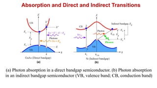
- 1. Absorption and Direct and Indirect Transitions (a) Photon absorption in a direct bandgap semiconductor. (b) Photon absorption in an indirect bandgap semiconductor (VB, valence band; CB, conduction band)
- 2. ) eV ( 24 . 1 ) μm ( g g E Absorption and the Bandgap Absorption cutoff wavelength Bandgap in eV Wavelength in microns (micrometers) Wavelengths greater than roughly g are not absorbed (by band-to band transitions)
- 3. Absorption Coefficient a I(x) = Ioexp(–ax) d = 1/a = penetration or absorption depth
- 4. Indirect Bandgap Semiconductors hkCB – hkVB = Phonon momentum = hK Photon energy absorbed hu = Eg h Phonon frequency Photon energy absorbed, hu = Eg h Phonon energy, small e.g. less than 0.1 eV
- 5. Semiconductors Semiconductor Eg (eV) g (eV) Type InP 1.35 0.91 D GaAs0.88Sb0.12 1.15 1.08 D Si 1.12 1.11 I In0.7Ga0.3As0.64P0.36 0.89 1.4 D In0.53Ga0.47As 0.75 1.65 D Ge 0.66 1.87 I InAs 0.35 3.5 D InSb 0.18 7 D Band gap energy Eg at 300 K, cut-off wavelength g and type of bandgap (D = Direct and I = Indirect) for some photodetector materials
- 6. photons incident of Number collected and generated EHP free of Number e External quantum efficiency (QE) e of the detector u h P e I o ph e / /
- 8. Responsivity R Si photodiodes of various sizes (S1336 series). (Courtesy of Hamamatsu)
- 9. EXAMPLE: Quantum efficiency and responsivity Consider the photodiode shown in Figure 5.7. What is the QE at peak responsivity? What is the QE at 450 nm (blue)? If the photosensitive device area is 1 mm2, what would be the light intensity corresponding to a photocurrent of 10 nA at the peak responsivity? Solution The peak responsibility in Figure 5.7 occurs at about 940 nm where R 0.56 A W-1. Thus, from Eq. (5.4.4), that is R =ee / hc, we have i.e. e = 0.74 or 74% We can repeat the calculation for = 450 nm, where R 0.24 AW-1, which gives e = 0.66 or 66%. From the definition of responsivity, R = Iph /Po, we have 0.56 AW-1 = (10×10-9 A)/Po, i.e. Po = 1.8×10⁻⁸ W or 18 nW. Since the area is 1 mm2 the intensity must be 18 nW mm-2. 19 9 1 34 8 -1 (1.6 10 C)(940 10 m) 0.56AW (6.63 10 J s )(3 10 m s ) e
- 10. External Quantum Efficiency and Responsivity Different contributions to the photocurrent Iph. Photogeneration profiles corresponding to short, medium and long wavelengths are also shown. Schematic photogeneration profiles
- 11. Internal Quantum Efficiency i photons absorbed of Number ated photogener EHP of Number y Efficienc Quantum Internal i Assuming lp is very thin, and assuming W >> Lh )] exp( 1 [ ) 0 ( W h P e I o i ph a u T T = Transmission coefficient of AR coating a = Absorption coefficient
- 12. pin Photodiode
- 13. The simple pn junction has two drawback. 1. Its junction or depletion layer capacitance is not sufficiently to allow photodetection at high modulation frequencies 2. Its depletion is at most a few microns – At long wavelength, the penetration depth is greater than the depletion layer width where there is no field to separate the EHPs & drift them – QE is correspondingly low at these long wavelengths • These problems are substantially reduced in the pin photodiode.
- 14. pin photodiode • pin refers to a device that has the structure p+-intrinsic-n+ as illustrated in fig. • In the idealized pin diode, the i-Si region is truly intrinsic – It is much wider than p+ & n+ regions (5-50m) • When the structure is first formed, – Holes diffuse from the p+-side and electrons from n+-side into the i-Si layer where they recombine and disappear. – This leaves a thin layer of negatively charged acceptor ions in the p+- side and positively donor ions in the n+-side. – The two charges are separated by the i-Si layer of thickness W • There is a uniform built-in field Eo in i-Si layer from the exposed positive ions to exposed negative ions
- 15. p+ i-Si n+ SiO2 Electrode – eNa net eNd (b) x (a) (a) The schematic structure of an idealized pin photodiode (b) The net space charge density across the photodiode. Electrode pin photodiode
- 16. x E(x) R Eo E h+ e– Iph hγ >E g W (c) (d) Vr Vout pin photodiode (c) The built-in field across the diode. (d) The pin photodiode in photo detection is reverse biased.
- 17. pin Photodiode (a)The schematic structure of an idealized pin photodiode (b) The net space charge density across the photodiode. (c) The built-in field across the diode. (d) The pin photodiode reverse biased for photodetection. Si pin InGaAs pin Courtesy of Hamamatsu
- 18. pin Photodiode W V W V r r o E E W A C r o dep d W t v drift
- 19. Depletion Layer Capacitance • The separation of two very thin layers of negative and positive charges by a fixed distance, width W of the i-Si, is the same as that in a parallel plate capacitor • The junction depletion or depletion layer capacitance of the pin diode is given by where A is the cross sectional area and or is the permittivity of the semiconductor (Si) • Since W is fixed by the structure, the junction capacitance does not depend on applied voltage • Cdep is typically of the order of a pF in fast pin photodiodes so that a 50 resistor, the RCdep time constantis about 50 ps. W or A Cdep
- 20. Reverse bias • When a reverse bias voltage Vr is applied across the pin device, it drops almost entirely across the width of i-Si layer. – The depletion widths in the p+ and n+ sides are negligible compared width W – The reverse bias increases the built-in voltage to Vo+Vr. – The field E in the i-Si layer is still uniform and increase to Vr Vo Vr Vr W W E E o
- 21. Response time • The pin structure is designed so that photon absorption occurs over the i-Si layer – The photogenerated EHPs are then separated by the field E and drifted towards the n+ and p+ sides respectively. • While the photogenerated carriers are drifting through the i-Si layer they give rise to an external photocurrent – which is detected as a voltage across a small resistor R • The response time of the pin diode is determined by the transit time of the carriers across the width W. – Increasing W allows more photons to be absorbed which increases the QE but it slow down the speed of response – because carrier transit time become longer
- 22. Transit time of carrier • For a charge carrier that is photogenerated at the edge on the i-Si, the transit time or drift time tdrift across the i-Si layer is • To reduce the drift time, that is increase the speed of response, – we have to increase vd and therefore increase the applied field E. d where v is its drift velocity d drift v t W ,
- 23. Drift velocity vs electric field in Si • Fig. shows the variation of the drift velocity of electrons and holes with the field in Si • The dE behavior is only observed at low field – Where d is the drift mobility • At high field, vd does not follow the expected dE behavior – both velocities tend to saturate at vsat which is of the order of 105ms–1 at field greater than 106Vm–1 • For an i-Si layer of width 10m, with carriers drifting as saturation velocities, the drift time is about 0.1ns which is longer than RCdep time constant – The speed of pin diodes are invariably limited by the transit time
- 24. Drift velocity vs. electric field for holes and electrons in Si. d W t v drift Width of i-region (Depletion region) Drift velocity Transit time (Drift time) Drift velocity vs electric field in Si
- 25. Example: Operation and speed of a pin photodiode • A Si pin photodiode has an i-Si layer of width 20m. The p+ layer on the illumination side is very thin 0.1m. The pin is reverse biased by a voltage of 100V and then illuminated with a very short optical pulse of wavelength 900nm. What is the duration of the photocurrent if absorption occurs over the whole i-Si layer?
- 26. Solution • The absorption coefficient at 900nm is ~3104m–1 so that the absorption depth is ~33m. We assume that absorption and hence photogeneration occurs over the entire width W of the i-Si layer. The field in the Si layer is E Vr/W = (100V)/(2010–6m) = 5106Vm–1 • At this field the electron drift velocity ve is very near its saturation at 105ms–1, whereas the hole drift velocity vh is about 7104ms–1. Holes are slightly slower than the electrons. The transit time th of holes across the i-Si layer is th W/vh = (2010–6m)/(7104ms–1) = 2.8610–10s • This is the response time of the pin as determined by the transit time of the slowest carriers, holes, across the i-Si layer. To improve the response time the width of the i-Si layer has to be narrowed but this decreases the quantity of absorbed photons and hence reduces the responsivity. There is therefore a trade off between speed and responsitivity.
- 27. Example: Responsivity of a pin photodiode • A Si pin photodiode has an active light receiving area of diameter 0.4mm. When radiation of wavelength 700nm (red light) and intensity 0.1mWcm–2 is incident, it generates a photocurrent of 56.6nA. What is responsivity and QE of the photodiode at 700nm?
- 28. Solution TheQE can be foundfrom The responsivityis The incident light intensity I 0.1mWcm-2 means that theincidentpower for conversionis 0.80 80% 1.61019 C700109 m 1 6.621034 Js3108 ms1 0.45AW hc R e 1 9 7 56.610 A/1.2610 W 0.45AW R I / P ph o 2 3 2 7 0.02cm 110 Wcm 1.2610 W o P AI
- 29. pin Photodiode Speed A reverse biased pin photodiode is illuminated with a short wavelength light pulse that is absorbed very near the surface. The photogenerated electron has to diffuse to the depletion region where it is swept into the i- layer and drifted across. In time t, an electron, on average, diffuses a distance l given by l = (2Det)1/2 Electron diffusion coefficient
- 30. pin Photodiode The responsivity of Si, InGaAs and Ge pin type photodiodes. The pn junction GaP detector is used for UV detection. GaP (Thorlabs, FGAP71), Si(E), IR enhanced Si (Hamamatsu S11499), Si(C), conventional Si with UV enhancement, InGaAs (Hamamatsu, G8376), and Ge (Thorlabs, FDG03). The dashed lines represent the responsivity due to QE = 100 %, 75% and 50 %.
- 31. Responsivity R depends on the device structure Two Si pin photodiodes with different device structures. A has UV response
- 32. Responsivity R depends on the temperature Responsivity of an InAs photodiode at two temperatures
- 33. EXAMPLE: Responsivity of a pin photodiode A Si pin photodiode has an active light receiving area of diameter 0.4 mm. When radiation of wavelength 700 nm (red light) and intensity 0.1 mW cm-2 is incident, it generates a photocurrent of 56.6 nA. What is the responsivity and external QE of the photodiode at 700 nm? Solution The incident light intensity I = 0.1 mW cm-2 means that the incident power for conversion is Po = AI = [(0.02 cm)2](0.110-3 W cm-2) = 1.2610-7 W or 0.126 W. The responsivity is R = Iph /Po = (56.6 10-9 A)/(1.2610-7 W ) = 0.45 A W-1 The QE can be found from % 80 80 . 0 m) 10 C)(700 10 (1.6 ) s m 10 s)(3 J 10 (6.62 ) W A 45 . 0 ( 9 19 -1 8 -34 1 - e hc R
- 34. EXAMPLE: Operation and speed of a pin photodiode A Si pin photodiode has an i-Si layer of width 20 m. The p+-layer on the illumination side is very thin (0.1 m). The pin is reverse biased by a voltage of 100 V and then illuminated with a very short optical pulse of wavelength 900 nm. What is the duration of the photocurrent if absorption occurs over the whole i-Si layer? Solution From Figure 5.5 , the absorption coefficient at 900 nm is ~ 3104 m-1 so that the absorption depth is ~33 m. We can assume that absorption and hence photogeneration occurs over the entire width W of the i-Si layer. The field in the i-Si layer is E Vr / W = (100 V)/(2010-6 m) = 5106 V m-1 Note: The absorption coefficient is between 3104 m-1 and 4104 m-1
- 35. At this field the electron drift velocity ve is very near its saturation at 105 m s-1, whereas the hole drift velocity vh, 7104 m s-1 as shown in Figure 5.10. Holes are slightly slower than the electrons. The transit time th of holes across the i-Si layer is th = W/vh = (2010-6 m)/(7104 m s-1) = 2.8610-10 s or 0.29 ns This is the response time of the pin as determined by the transit time of the slowest carriers, holes, across the i-Si layer. To improve the response time, the width of the i-Si layer has to be narrowed but this decreases the quantity of photons absorbed and hence reduces the responsivity. There is therefore a trade off between speed and responsivity. EXAMPLE: Operation and speed of a pin photodiode Solution (continued)
- 36. EXAMPLE : Photocarrier Diffusion in a pin photodiode A reverse biased pin photodiode is illuminated with a short wavelength light pulse that is absorbed very near the surface. The photogenerated electron has to diffuse to the depletion region where it is swept into the i-layer and drifted across by the field in this region. What is the speed of response of this photodiode if the i-Si layer is 20 m and the p+-layer is 1 m and the applied voltage is 60 V? The diffusion coefficient (De) of electrons in the heavily doped p+-region is approximately 310-4 m2 s-1. Solution There is no electric field in the p+-side outside the depletion region as shown in Figure 5.12 . The photogenerated electrons have to make it across to the n+-side to give rise to a photocurrent. In the p+-side, the electrons move by diffusion. In time t, an electron, on average, diffuses a distance l given by l = [2Det]1/2 The diffusion time tdiff is the time it takes for an electron to diffuse across the p+-side (of length l ) to reach the depletion layer and is given by
- 37. EXAMPLE: Photocarrier Diffusion in a pin photodiode Solution (continued) tdiff = l 2/(2De) = (110-6 m)2 / [2(310-4 m2 s-1)] = 1.6710-9 s or 1.67 ns. On the other hand, once the electron reaches the depletion region, it becomes drifted across the width W of the i-Si layer at the saturation drift velocity since the electric field here is E = Vr / W = 60 V / 20 m = 3106 V m- 1; and at this field the electron drift velocity ve saturates at 105 m s-1. The drift time across the i-Si layer is tdrift = W / ve = (2010-6 m) / (1105 m s-1) = 2.010-10 s or 0.2 ns. Thus, the response time of the pin to a pulse of short wavelength radiation that is absorbed near the surface is very roughly tdiff + tdrift or 1.87 ns. Notice that the diffusion of the electron is much slower than its drift. In a proper analysis, we have to consider the diffusion and drift of many carriers, and we have to average (tdiff + tdrift) for all the electrons.
- 38. EXAMPLE: Steady state photocurrent in the pin photodiode Consider a pin photodiode that is reverse biased and illuminated, as in Figure 5.9, and operating under steady state conditions. Assume that the photogeneration takes place inside the depletion layer of width W, and the neutral p-side is very narrow. If the incident optical power on the semiconductor is Po(0), then TPo(0) will be transmitted, where T is the transmission coefficient. At a distance x from the surface, the optical power Po(x) = TPo(0)exp(ax). In a small volume dx at x, the absorbed radiation power (by the definition of a) is aPo(x)dx, and the number of photons absorbed per second is aPo(x)dx /hu. Of these absorbed photons, only a fraction i will photogenerate EHPs, where i is the internal quantum efficiency IQE. Thus, iaPo(x)dx /hu number of EHPs will be generated per second.
- 39. EXAMPLE: Steady state photocurrent in the pin photodiode We assume these will drift through the depletion region and thereby contribute to the photocurrent. The current contribution d Iph from absorption and photogeneration at x within the SCL will thus be We can integrate this from x = 0 (assuming lp is very thin) to the end of x = W, and assuming W >> Lh to find Steady state photocurrent pin photodiode (5.5.4) where the approximate sign embeds the many assumptions we made in deriving Eq. (5.5.4). Consider a pin photodiode without an AR coating so that T = 0.68. Assume i = 1. The SCL width is 20 m. If the device is to be used at 900 nm, what would be the photocurrent if the incident radiation power is 100 nW? What is the responsivity? Find the photocurrent and the responsivity if a perfect AR coating is used. What is the primary limiting factor? What is the responsivity if W = 40 µm? x x h P e h x x P e δI o i o i ph d a u a u d a ) exp( ) 0 ( ) ( T )] exp( 1 [ ) 0 ( W h P e I o i ph a u T
- 40. EXAMPLE: Steady state photocurrent in the pin photodiode Solution (continued) From Figure 5.5, at = 900 nm, a 3 ×10⁴ m-1. Further for =0.90 m, the photon energy hu = 1.24 / 0.90 = 1.38 eV. Given Po(0) = 100 nW, we have = 22 nA and the responsivity R = 22 nA / 100 nW = 0.22 A W-1, which is on the low-side. Consider next, a perfect AR coating so that T = 1, and using Eq. (5.5.4) again, we find Iph = 32.7 nA and R = 0.33 A W-1, a significant improvement. The factor [1exp(aW)] is only 0.451, and can be significantly improved by making the SCL thicker. Setting W = 40 m, gives [1exp(aW)] = 0.70 and R = 0.51, which is close to values for commercial devices. The maximum theoretical photocurrent would be obtained by setting exp(aW) 0, T = 1, i = 1, which gives Iph = 73 nA and R = 0.73 A W-1. )] 10 20 10 3 exp( 1 [ ) 10 6 . 1 38 . 1 ( ) 10 100 )( 68 . 0 )( 1 )( 10 6 . 1 ( 6 4 19 9 19 ph I
- 42. Avalanche Photodiode (APD) • APDs are widely used in optical communications due to their high speed and internal gain. • The n+ side is thin and it is the side that is illuminated through a window. • There are three p-type layers of different doping levels next to n+ layer to suitably modify the field distribution across the diode – The first is a thin p-type layer – The second is a thick lightly p-type doped -layer – The third is a heavily doped p+ layer
- 43. p+ SiO2 Electrode net x E(x) R E hu >E g p Iph e– h+ (a) (b) (c) x Absorption region Avalanche region Electrode n+ Avalanche Photodiode (a) A schematic illustration of the structure of an avalanche photodiode (APD) biased for avalanche gain. (b) The net space charge density across the photodiode. (c) The field across the diode and the identification of absorption and multiplication regions.
- 44. Reverse bias • The diode is reverse biased to increase the fields in the depletion regions • Under zero bias, the depletion layer in the p-region does not normally extend across this layer to the - layer. • But when a sufficient reverse bias is applied, the depletion region in the p-layer widens to reach- through to the -layer – The field extends from the exposed positively charged donors in the thin depletion layer in n+ side, all the way to the exposed negatively charged acceptors in the thin depletion layer in p+- side.
- 45. Electric field • The electric field is given by the integration of the net space charge density net across the diode is shown in Fig. • The field lines start at positive ions and end at negative ions, which exist through the p, & p+ layers. –It is maximum at n+p junction, then decreases slowly through the p layer. –Through the -layer, it decreases slightly as the net space charge here is small –The field vanishes at the end of the narrow depletion layer in the p+ side.
- 46. Avalanche of impact ionization processes • The absorption of photons and photogeneration mainly occur in the long -layer. – The nearly uniform field here separates the EHPs and drifts them at velocities near saturation towards the n+ and p+ sides respectively. • When the drifting electrons reach p-layer, they experience even greater fields – therefore acquire sufficient kinetic energy (>Eg) to impact-ionize some of the Si covalent bonds and release EHPs. – These generated EHPs also be accelerated by the high fields to sufficiently large kinetic energies to further cause impact ionization and release more EHPs – It leads to an avalanche of impact ionization processes. – Thus, a single electron entering the p-layer can generate a large number of EHPs, which contribute to observed photocurrent.
- 47. (a) A pictorial view of impact ionization processes releasing EHPs and the resulting avalanche multiplication. (b) Impact of an energetic conduction electron with crystal vibrations transfers the electron's kinetic energy to a valence electron and thereby excites it to the conduction band. E š n+ p h+ e– Avalanche region (a) e– h+ Ec Ev (b) E Avalanche of impact ionization processes
- 48. Internal gain mechanism • A single photon absorption leads to a large number of EHPs generated called internal gain mechanism • The photocurrent with the presence of avalanche multiplication – can has an effective quantum efficiency in excess of unity • The reason for keeping the photogeneration within -region and reasonably separated from the avalanche p-region is that – Avalanche multiplication is a statistical process and hence leads to carrier generation fluctuation, which leads to excess noise in the avalanche multiplied photocurrent. – This is minimized if impact ionization is restricted to the carrier with the highest impact ionization efficiency which is the electron.
- 49. Avalanche multiplication factor whereIph is the APD photocurrent that has been multiplied and I pho is the primary or unmultiplied photocurrent that is measured in the absenceof multiplication (under small reversebias Vr ) The overall avalanchemultiplication factorM of an APD is defined as, Ipho Primaryunmultiplied photocurrent Multiplied photocurrent Iph M
- 50. M function • The multiplication of carriers in the avalanche region depends on the probability of impact ionization, – which depends strongly on the field in this region and hence on the reverse bias Vr • The multiplication M is a strong function of the reverse bias and also the temperature • For Si APDs, M values can be as high as 100, but for many commercial Ge APDs, M are typically around 10.
- 51. Empirical avalanche multiplication factor Where Vbr is a parameter called the avalanche breakdown voltage n is a characteristic index that provides the best fit to the experimental data Vbr and n are strongly temperature dependent Empirical expression m r V V M br 1 1
- 52. Avalanche Photodiode Gain or Multiplication M Ionization coefficient ratio αe = Aexp(-B/E) Chyoweth's law
- 53. Avalanche Photodiode Gain or Multiplication M M = exp(aew) Ionization coefficient k w k k M e ] ) 1 ( exp[ 1 a Electrons only Electrons and holes k ah / ae
- 54. Speed of the reach-through APD • The speed of the reach-through APD depends on three factors 1. The time it takes for the photogenerated electron to cross the absorption region (-layer) to the multiplication region (p-layer) 2. The time it takes for the avalanche process to build up in the p-region and generate EHPs 3. The time it takes for the last hole released in the avalanche process to transit through the -region
- 55. Speed of photodetector • The response time of an APD to an optical pulse is longer than a corresponding pin structure – But, in practice, the multiplication gain makes up for the reduction in the speed. • The overall speed of a photodetector circuit – includes limitation from the electronic pre-amplifier connected to the photodetector. • The APD requires less subsequent electronic amplication – Which translates to an overall speed that can be faster than a corresponding detector circuit using a pin photodiode
- 56. Example: InGaAs APD responsivity • An InGaAs APD has a quantum efficiency (QE) of 60% at 1.55m in the absence of multiplication (M=1). It is biased to operate with a multiplication of 12. Calculate the photocurrent if the incident optical power is 20nW. What is the responsivity when the multiplication is 12?
- 57. Solution 1 6.6261034 3108 0.75AW Theresponsivity M 12 is The photodiodecurrentIph in theAPD willbe Ipho multiplied by M, The responsivity at M 1in terms of the quantum efficiency is 12 1.5108 A1.8107 A I ph MIpho 12 0.75 1 / P MR 9.0AW R= Iph o 1 9 8 I RP 0.75AW 2010 W 1.510 A pho o If I ph is theprimary photocurrent (unmultiplied) and Pois theincident optical power then by definition R I ph/ Po so that e 1.61019 1550109 R 0.6 hc
- 58. Avalanche Photodiode Typical multiplication (gain) M vs. reverse bias characteristics for a typical commercial Si APD, and the effect of temperature. (M measured for a photocurrent generated at 650 nm of illumination)
- 59. Avalanche Photodiode (a) A Si APD structure without a guard ring. (b) A schematic illustration of the structure of a more practical Si APD. Note: SiO2 is silicon dioxide and serves as an insulating passivation layer.
- 60. Photodiode Comparison Photodiode range peak R at peak Gain Id For 1 mm2 Features nm nm A/W GaP pin 150550 450 0.1 <1 1 nm UV detectiona GaAsP pn 150750 500720 0.20.4 <1 0.0050.1 nA UV to visible, covering the human eye, low Id. GaAs pin 570870 850 0.50.5 <1 0.11 nA High speed and low Id Si pn 2001100 600900 0.50.6 <1 0.0050.1 nA Inexpensive, general purpose, low Id Si pin 3001100 8001000 0.50.6 <1 0.11 nA Faster than pn Si APD 4001100 800900 0.40.6b 10103 110 nAc High gains and fast Ge pin 7001800 15001580 0.40.7 <1 0.11 A IR detection, fast. Ge APD 7001700 15001580 0.40.8b 1020 110 Ac IR detection, fast InGaAs pin 8001700 15001600 0.71 <1 150 nA Telecom, high speed, low Id InGaAs APD 8001700 15001600 0.70.95b 1020 0.0510 Ac Telecom, high speed and gain. InAs pn 23.6 m 3.03.5 m 11.5 <1 >100 A Photovoltaic mode. Normally cooled InSb pn 45.5 m 5 m 3 <1 Large Photovoltaic mode. Normally cooled NOTE: cFGAP71 (Thorlabs); aAt M = 1; cAt operating multiplication.
- 62. Simplified schematic diagram of a separate absorption and multiplication (SAM) APD using a heterostructures based on InGaAs-InP. P and N refer to p and n -type wider-bandgap semiconductor. Heterojunction Photodiodes: SAM
- 63. Heterojunction Photodiodes: SAM (a)Energy band diagrams for a SAM detector with a step junction between InP and InGaAs. There is a valence band step ΔEv from InGaAs to InP that slows hole entry into the InP layer. (b)An interposing grading layer (InGaAsP) with an intermediate bandgap breaks ΔEv and makes it easier for the hole to pass to the InP layer for a detector with a graded junction between InP and InGaAs. This is the SAGM structure.
- 64. Heterojunction Photodiodes: SAM Simplified schematic diagram of a more practical mesa-etched SAGM layered APD
- 65. APD Characteristics Typical current and gain (M) vs. reverse bias voltage for a commercial InGaAs reach-through APD. Id and Iph are the dark current and photocurrent respectively. The input optical power is ~100 nW. The gain M is 1 when the diode has attained reach-through and then increases with the applied voltage. (The data extracted selectively from Voxtel Catalog, Voxtel, Beaverton, OR 97006)
- 66. EXAMPLE: InGaAs APD Responsivity An InGaAs APD has a quantum efficiency (QE, e) of 60 % at 1.55 m in the absence of multiplication (M = 1). It is biased to operate with a multiplication of 12. Calculate the photocurrent if the incident optical power is 20 nW. What is the responsivity when the multiplication is 12? Solution The responsivity at M = 1 in terms of the quantum efficiency is = 0.75 A W-1 If Ipho is the primary photocurrent (unmultiplied) and Po is the incident optical power then by definition, R = Ipho/Po so that Ipho = RPo = (0.75 A W-1)(2010-9 W) = 1.510-8 A or 15 nA. The photocurrent Iph in the APD will be Ipho multiplied by M, Iph = MIpho = (12)(1.510-8 A) = 1.8010-7 A or 180 nA. The responsivity at M = 12 is R = Iph /Po = MR = (12) / (0.75) = 9.0 A W-1 19 9 34 8 -1 (1.6 10 C)(1550 10 m) (0.6) (6.626 10 J s)(3 10 m s ) e e hc R
- 67. EXAMPLE: Silicon APD A Si APD has a QE of 70 % at 830 nm in the absence of multiplication, that is M = 1. The APD is biased to operate with a multiplication of 100. If the incident optical power is 10 nW what is the photocurrent? Solution The unmultiplied responsivity is given by, = 0.47 A W-1 The unmultiplied primary photocurrent from the definition of R is Ipho = RPo = (0.47 A W-1)(1010-9 W) = 4.7 nA The multiplied photocurrent is Iph = MIpho = (100)(4.67 nA ) = 470 nA or 0.47 A 19 9 34 8 -1 (1.6 10 C)(830 10 m) (0.70) (6.626 10 J s)(3 10 m s ) e e hc R
- 68. EXAMPLE: Avalanche multiplication in Si APDs The electron and hole ionization coefficients ae and ah in silicon are approximately given by Eq. (5.6.4) with A 0.740×106 cm-1, B 1.16×10⁶ V cm-1 for electrons (ae) and A 0.725×106 cm-1 and B 2.2×10⁶ V cm-1 for holes (ah). Suppose that the width w of the avalanche region is 0.5 m. Find the multiplication gain M when the applied field in this region reaches 4.00×10⁵ V cm-1, 4.30×10⁵ V cm-1 and 4.38×10⁵ V cm-1 . What is your conclusion? Solution At the field of E = 4.00×10⁵ V cm-1, from Eq. (5.6.4) ae = Aexp(B/E) = (0.74×106 cm-1)exp[1.16×10⁶ V cm-1)/(4.00×105 V cm-1)] = 4.07×104 cm-1. Similarly using Eq. (5.6.4) for holes, ah = 2.96×103 cm-1. Thus k = ah /ae = 0.073. Using this k and ae above in Eq. (5.6.6) with w = 0.5×10⁻⁴ cm, = 11.8 Note that if we had only electron avalanche without holes ionizing, then the multiplication would be Me = exp (aew) = exp[(4.07×104 cm-1)(0.5×10⁻⁴ cm)] = 7.65 073 . 0 )] cm 10 5 . 0 )( cm 10 07 . 4 )( 073 . 0 1 ( exp[ 073 . 0 1 1 - 4 4 M
- 69. EXAMPLE: Avalanche multiplication in Si APDs Solution (contiued) We can now repeat the calculations for E = 4.30×10⁵ V cm-1 and again for E = 4.38×10⁵ V cm-1. The results are summarized in Table 5.3 for both M and Me. Notice how quickly M builds up with the field and how a very small change at high fields causes an enormous change in M that eventually leads to a breakdown. (M running away to infinity as Vr increases.) Notice also that in the presence of only electron-initiated ionization, Me simply increases without a sharp run-away to breakdown. E (V cm-1) ae (cm-1) ah (cm-1) k M Me Comment 4.00×10⁵ 4.07×10⁴ 2.96×10³ 0.073 11.8 7.65 M and Me not too different at low E 4.30×10⁵ 4.98×10⁴ 4.35×10³ 0.087 57.2 12.1 7.5% increase in E, large difference between M and Me 4.38×10⁵ 5.24×10⁴ 4.77×10³ 0.091 647 13.7 1.9% increase in E
- 70. Superlattice APD Multiple Quantum Well Detectors (a) Energy band diagram of a MQW superlattice APD. (b) Energy band diagram with an applied field and impact ionization.
- 72. Schottky Junction Photodiodes GaAsP Schottky junction photodiode for 190-680 nm detection, from UV to red (Courtesy of Hamamatsu) GaP Schottky junction photodiode for 190 nm to 550 nm detection. (Courtesy of Hamamatsu) Schottky kunction type metal-semiconductor-metal (MSM) type photodetectors. (Courtesy of Hamamatsu) AlGaN Scottky junction photodiode for UV detection (Courtesy of sglux, Germany)
- 73. Schottky Junction (a) Metal and an n-type semiconductor before contact. The metal work function Fm is greater than that of the n-type semiconductor (b) A Schottky junction forms between the metal and the semiconductor. There is a depletion region in the semiconductor next to the metal and a built-in field Eo (c) Typical I vs. V characteristics of a Schottky contact device.
- 74. Reverse biased Schottky junction and the dark current due to the injection of electrons from the metal into the semiconductor over the barrier FB. Schottky Junction
- 75. LEFT: Photogeneration in the depletion region and the resulting photocurrent. RIGHT: The Schottky junction photodetector Schottky Junction
- 76. Schottky Junction Photodiodes Schottky junction range nm Rpeak (at peak) (A/W) Jdark per mm2 Features with typical values GaAsP 190680 0.18 (610 nm) 5 pA UV to red, tR = 3.5 s. (G1126 seriesa) GaP 190550 0.12 (440 nm) 5 pA UV to green, tR = 5 s. (G1961a) AlGaN 220375 0.13 (350 nm) 1 pA Measurement of UV; blind to visible light. (AG38Sb) GaAs 320900 0.2 (830 nm) ~ 1 nA Wide bandwidth > 10 GHz, tR < 30 ps. (UPD-30- VSG-Pc) InGaAs MSM 8501650 0.4 (1300 nm) 5 A Optical high speed measurements, tR = 80 ps, tF = 160 ps. (G7096a) GaAs MSM 450870 0.3 (850 nm) 0.1 nA Optical high speed measurements, tR = 30 ps, tF = 30 ps. (G4176a) Schottky junction based photodetectors and some of their features. tR and tF are the rise and fall times of the output of the photodetector for an optical pulse input. The rise and fall times represent the times required for the output to rise from 10% to 90% of its final steady state value and to fall from 90% to 10% of its value before the optical pulse is turned off. aHamamatsu (Japan); bsglux (Germany); cAlphalas
- 77. Schottky Junction Photodiodes LEFT: The metal electrodes are on the surface of the semiconductor crystal (which is grown on a suitable substrate). RIGHT: The electrodes are configured to be interdigital and on the surface of the crystal.
- 78. Schottky Junction Photodiodes LEFT: Two neighboring Schottky junctions are connected end-to-end, but in opposite directions as shown for A and B. The energy band diagram without any bias is symmetrical. The grey areas represent the SCL1 and SCL2 at A and B. RIGHT: Under a sufficiently large bias, the SCL1 from A extends and meets that from B so that the whole semiconductor between the electrodes is depleted. There is a large field in this region, and the photogenerated EHPs become separated and then drifted, which results in a photocurrent.
- 79. Phototransistor
- 80. Phototransistor IE exp(eVBE/kBT) Iph bIpho Transistor action Gain
- 81. Photoconductive Detectors PbS (lead sulfide) photoconductive detectors for the detection of IR radiation up to 2.9 m. They are typically used in such applications as radiation thermometers, flame monitors, water content and food ingredient analyzers, spectrophotometers etc.. (P9217 series) (Courtesy of Hamamatsu.)
- 82. Photoconductive (PC) Detectors Photodiode PbS (PC) 10C PbSe (PC) 10 C InSb (PC) 10C peak (m) 2.4 4.1 5.5 Id or Rd 0.11 M 0.11 M 110 k NEP W Hz-1/2 - - D* cm Hz1/2/ W 1×10⁹ 5×10⁹ 1×10⁹ Used for radiation measurement at long wavelengths PbS photoconductive detectors (Courtesy of Hamamatsu)
- 83. Photoconductive (PC) Detectors Used for radiation measurement at long wavelengths PbS photoconductive detectors (Courtesy of Hamamatsu)
- 84. Photoconductive (PC) Detectors The basic principle in photoconductive detectors is the change in the resistance of the semiconductor upon exposure to light. The photoconductor (PC) has a dark resistance Rd and is biased by VB through a load RL. A chopper (either mechanical or electronic) chops the light at a frequency fc. The resistance of the PC changes periodically at the chopper frequency. The photocurrent generates a varying voltage signal vph(t) across Rd, which can be coupled through a coupling capacitor into a lock-in amplifier LIA. This amplifier is synchronized with the chopper and only amplifies the signal if it is in phase with the chopper. Its output is a dc signal that represents the magnitude of vph that is in phase with the chopped light. The periodic change in Rd causes a period change in the current. This periodic change is the photocurrent iph(t) signal and is an ac-type signal at the frequency fc.
- 85. Photoconductive Detectors A semiconductor slab of length l, width w and depth d is illuminated with light of wavelength
- 86. Photoconductive Detectors A photoconductor with ohmic contacts (contacts not limiting carrier entry) can exhibit gain. As the slow hole drifts through the photoconductors, many fast electrons enter and drift through the photoconductor because, at any instant, the photoconductor must be neutral. Electrons drift faster which means as one leaves, another must enter.
- 87. Photoconductivity Ds and Photocurrent Density Jph Steady state illumination hcd d hv Ad A i i i I I g F ph ph Photon flux = Fph 0 ph D D t n dt n d g i = Internal quantum efficiency Ds = eeDn + ehDp = eDn(e + h) Photoconductivity hcd e h e i ) ( t s D I E s s D D l V Jph Photogeneration rate
- 88. Photoconductive Gain Photon flux = Fph hc w e wdJ e I h e i E I ) ( flow electron of Rate ph ph t hc w wd i I g g l l ph ph ) ( ) Volume ( generation electron of Rate Photoconductive gain G l E ) ( absorption light by generation electron of Rate circuit external in flow electron of Rate h e G t
- 89. Photoconductive Gain Photon flux = Fph l E ) ( absorption light by generation electron of Rate circuit external in flow electron of Rate h e G t Electron and hole transit times (time to cross the semiconductor) are te = l / (eE) th = l / (hE) e h e h e t t t G t t t 1 Electron Hole Photoconductive gain G
- 90. Basic Photodiode Circuits (a) The photodiode is reverse biased through RL and illuminated. Definitions of positive I and V are shown as if the photodiode were forward biased. (b) IV characteristics of the photodiode with positive I and V definitions in (a). The load line represents the behavior of the load R. The operating point is P where the current and voltage are I and V.
- 91. Basic Photodiode Circuits: The Load Line The current through RL is I = (V + Vr / RL This is the load line shown in the figure. P is the intersection of the load line with the photodiode I vs. V curve and is the operating point. P is the operating point V 3.5 V I 2.5 A I Iph
- 92. Basic Photodiode Circuits A simple circuit for the measurement of the photocurrent Iph by using a current-voltage converter or a transimpedance amplifier. The reverse bias Vr is a positive number. Note that biasing circuit for the op amp is not shown.
- 93. Photodiode Equivalent Circuit (a) A real photodiode has series and parallel resistances Rs and Rp and a SCL capacitance Cdep. A and C represent anode and cathode terminals. (b) The equivalent circuit of a photodiodes. For ac (or transient) signals, the battery can be shorted since ac signals will simply pass through the battery.
- 94. Reverse Biased Photodiode Equivalent Circuit Rs = Series resistance Rp = Shunt (parallel) resistance Ideal photodiode Total capacitance = ideal photodiode SCL capacitance + terminal capacitance
- 95. A Commercial Photoreceiver A photoreceiver that has an InGaAs APD and peripheral electronics (ICs) to achieve high gain and high sensitivity. There is also a thermoelectric cooler (TEC) and a temperature sensor (TSense). Courtesy of Voxtel Inc (www.voxtel-inc.com) APD Thermoelectric (TEC) cooler Op amp Output APD bias Temperature sensor (Tsense) TEC Current in direction TEC Current out direction Base/Collector Emitterr Op amp bias
- 96. Pulsed Excitation Large resistor to bias the PD Bias or shorting capacitor to short RB and the battery for the transient photocurrent. It is a short for ac/transient signals Load resistor for developing a voltage signal Very fast buffer or amplifier that does not load RL. Po(t) t Coupling capacitor that allows ac/transient signal coupling Reverse biases the PD PD Short light pulse
- 97. Pulsed Excitation Rise time Fall time Assume: The buffer is extremely fast and does not limit the response The Experiment Are these related to fc?
- 98. Rise and Fall Times, and Bandwidth Rise time Fall time Very roughly, tR tF V(t) V100exp(t/t) Measured from toff tF = 2.2t t = (Rs+ RL)Ct RLCt t = (Rs+ RL)Ct RLCt ) ns ( MHz 350 35 . 0 2 1 2 1 F F t L c C R f t t t
- 99. Pulsed Excitation Non-RLCt response Response due to the diffusion and drift of photogenerated carriers Assume Rs + RL is very small so that (Rs + RL)Ct is negligible Drift of carriers in the depletion region Diffusion of carriers in the neutral region Slow Fast Fast Slow t Photocurrent Drift of carriers in the depletion region Diffusion of carriers in the neutral region
- 101. Noise in Photodiodes Noise current = Total RMS current fluctuations Constant illumination What is the RMS of fluctuations? Consider a receiver with a photodiode and a sampling resistor RL The amplifier A is assumed noiseless Consider constant illumination Po Total current without noise = Dark current (Id) + Photocurrent (Iph) = “Constant” Observed Current = Dark current + Photocurrent and Fluctuations (Noise) What is this “Noise” ? 2 ) ( ns fluctuatio of RMS t i We can represent the “noise current” by the RMS of fluctuations i(t)
- 102. Noise in Photodiodes The dark current has shot noise or fluctuations about Id, in-dark = (2eIdB)1/2 Quantum noise is due to the photon nature of light and its effects are the same as shot noise. Photocurrent has quantum noise or shot noise B = Bandwidth in-quantum = (2eIphB)1/2 Noise current = Total RMS current fluctuations Constant illumination What is the RMS of fluctuations? i(t)
- 103. Noise in Photodiodes 2 quantum 2 dark 2 n n n i i i Total shot noise current, in in = [2e(Id + Iph)B]1/2 We can conceptually view the photodetector current as Id + Iph + in This flows through a load resistor RL and voltage across RL is amplified by A to give Vout The noise voltage (RMS) due to shot noise in PD = inRLA
- 104. Noise in Photodiodes Total current flowing into RL has three components: Id = Dark current. In principle, we can subtract this or block it with a capacitor if Iph is an ac (transient) signal. Iph = Photocurrent. This is the signal. We need this. It could be a steady or varying (ac or transient) signal. in = Total shot noise. Due to shot noise from Id and Iph. We cannot eliminate this.
- 105. Noise in Photodiodes 4 = from current noise Thermal 1/2 th L B L R TB k R i 4 = 2 TB k i R B L i2 L R i in Current The resistor RL exhibits thermal noise (Johnson noise) Power in thermal fluctuations in RL = 4kBTB
- 106. Summary of Noise in PD and RL Important Note: Total noise is always found by first summing the average powers involved in individual fluctuations e.g. power in shot noise + power in thermal noise Power in shot noise in PD = in 2RL = [2e(Id + Iph)B]RL Power in thermal fluctuations in RL = 4kBTB Noise in the amplifier A must also be included See advanced textbooks
- 107. Power Noise Power Signal SNR L B ph d ph B L n L ph R TB k B I I e I TB k R i R I 4 ) ( 2 4 SNR 2 2 2 Important Note: Total noise is always found by first summing the average powers involved in individual fluctuations e.g. power in shot noise + power in thermal noise Signal to Noise Ratio
- 108. Noise Equivalent Power: NEP 2 / 1 1 Bandwidth 1 SNR for power Input NEP B P Definition NEP is defined as the required optical input power to achieve a SNR of 1 within a bandwidth of 1 Hz 2 / 1 2 / 1 1 ) ( 2 1 NEP ph d I I e B P R Units for NEP are W Hz–1/2
- 109. Detectivity, D NEP 1 y Detectivit Definition Specific detectivity D* NEP * 2 / 1 A D Units for D* are cm Hz-1/2 W-1, or Jones
- 110. NEP and Detectivity of Photodetectors Photodiode GaP Schottky Si pin Ge pin InGaAs pin PbS (PC) 10C PbSe (PC) 10 C InSb (PC) 10C peak (m) 0.44 0.96 1.5 1.55 2.4 4.1 5.5 Id or Rd 10 pA 0.4 nA 3 A 5 nA 0.11 M 0.11 M 110 k NEP W Hz-1/2 5.4×10⁻¹⁵ 1.6×10⁻¹⁴ 1×10-12 4×10-14 - - D* cm Hz1/2/ W 1×10¹³ 1×10¹² 1×10¹¹ 5×10¹² 1×10⁹ 5×10⁹ 1×10⁹ Typical noise characteristics of a few selected commercial photodetectors. PC means a photoconductive detector, whose photoconductivity is used to detect light. For PC detectors, what is important is the dark resistance Rd, which depends on the temperature. 2 / 1 2 / 1 1 ) ( 2 1 NEP ph d I I e B P R
- 111. NEP and Dark Current The dependence of NEP (W Hz-1/2) on the photodetector dark current Id for Si and InGaAs pin, Ge pn junction, and GaP Schottky photodiodes. Dashed lines indicate observed trends. Filled circle, Si pin; open circle, InGaAs pin at 25 C, open diamond at 10 C, open square, 20 C; inverted triangle, Ge pn; triangle, GaAsP Schottky. (Data extracted from datasheets of 35 commercial photodiodes)
- 112. Noise in Avalanche Photodiode (APD) in-APD = Min = M[2e(Ido + Ipho)B]1/2 in-APD = [2e(Ido + Ipho)M2B]1/2 Ideally the shot noise is simply multiplied so that we should expect But, we observe excess noise above this shot noise Avalanche Noise in-APD = [2e(Ido + Ipho)M2FB]1/2 Excess Noise Factor
- 113. Noise in Avalanche Photodiode (APD) Excess Avalanche Noise Factor F in-APD = [2e(Ido + Ipho)M2FB]1/2 Excess Noise Factor APDs exhibit excess avalanche noise due to the randomness of the impact ionization process in the multiplication region. Some carriers travel far and some short distances within this zone before they cause impact ionization F Mx where x is an index that depends on the semiconductor, the APD structure and the type of carrier that initiates the avalanche (electron or hole) For Si APDs, x is 0.30.5 whereas for Ge and III-V (such as InGaAs) alloys it is 0.71
- 114. EXAMPLE: Noise of an ideal photodetector Consider an ideal photodiode with e = 1 (QE = 100%) and no dark current, Id = 0. Show that the minimum optical power required for a signal to noise ratio (SNR) of 1 is (5.12.9) Calculate the minimum optical power for a SNR = 1 for an ideal photodetector operating at 1300 nm with a bandwidth of 1 GHz? What is the corresponding photocurrent? Solution We need the incident optical power P1 that makes the photocurrent Iph equal to the noise current in, so that SNR = 1. The photocurrent (signal) is equal to the noise current when Iph = in =[2e(Id + Iph)B]1/2 = [2eIphB]1/2 since Id = 0. Solving the above, Iph = 2eB From Eqs. (5.4.3) and (5.4.4), the photocurrent Iph and the incident optical power P1 are related by Thus, B hc P 2 1 eB hc eP I e ph 2 1 B hc P e 2 1
- 115. For an ideal photodetector, e = 1 which leads to Eq. (5.12.9). We note that for a bandwidth of 1Hz, NEP is numerically equal to P1 or NEP = 2hc/. For an ideal photodetector operating at 1.3 m and at 1 GHz, P1 = 2hcB/e = 2(6.6310-34 J s)(3108 m s-1)(109 Hz) / (1)(1.310-6 m) = 3.110-10 W or 0.31 nW. This is the minimum signal for a SNR = 1. The noise current is due to quantum noise. The corresponding photocurrent is Iph = 2eB = 2(1.610-19 C)(109 Hz) = 3.210-10 A or 0.32 nA. Alternatively we can calculate Iph from Iph = eeP1 / hc with e = 1. EXAMPLE: Noise of an ideal photodetector Solution (continued)
- 116. Solution By definition, NEP is that optical power per square root of bandwidth which generates a photocurrent equal to the noise current in the detector. NEP = P1/B1/2 Thus, P1 = NEPB1/2 = (10-13 W Hz -1/2)(109 Hz)1/2 = 3.1610-9 W or 3.16 nW EXAMPLE: NEP of a Si pin photodiode A Si pin photodiode has a quoted NEP of 110-13 W Hz-1/2. What is the optical signal power it needs for a signal to noise ratio (SNR) of 1 if the bandwidth of operation is 1GHz?
- 117. EXAMPLE: SNR of a receiver Consider an InGaAs pin photodiode used in a receiver circuit as in Figure 5.31 with a load resistor of 10 k. The photodiode has a dark current of 2 nA. The bandwidth of the photodiode and the amplifier together is 1 MHz. Assuming that the amplifier is noiseless, calculate the SNR when the incident optical power generates a mean photocurrent of 5 nA (corresponding to an incident optical power of about 6 nW since R is about 0.80.9 nA/nW at the peak wavelength of 1550 nm). Solution The noise generated comes from the photodetector as shot noise and from RL as thermal noise. The mean thermal noise power in the load resistor RL is 4kBTB. If Iph is the photocurrent and in is the shot noise in the photodetector then The term 4kBTB/RL in the denominator represents the mean square of the thermal noise current in the resistor. We can evaluate the magnitude of each noise current by substituting, Iph = 5 nA, Id = 2 nA, B = 1 MHz, RL = 104 , T = 300 K. 2 2 2 Signal Power SNR Noise Power 4 2 ( ) 4 / ph L ph n L B d ph B L I R I i R k TB e I I B k TB R
- 118. EXAMPLE: SNR of a receiver Solution (continued) Shot noise current from the detector = [2e(Id + Iph)B]1/2 = 0.047 nA = 1.29 nA Thus, the noise contribution from RL is greater than that from the photodiode. The SNR is = 15.0 Generally SNR is quoted in decibels. We need 10log(SNR), or 10log(15.0) i.e., 11.8 dB. Clearly, the load resistance has a dramatic effect on the overall noise performance. 2 9 2 9 2 9 ) A 10 29 . 1 ( ) A 10 047 . 0 ( ) A 10 5 ( SNR
- 119. EXAMPLE: Noise in an APD Consider an InGaAs APD with x 0.7 which is biased to operate at M = 10. The unmultiplied dark current is 10 nA and bandwidth is 700 MHz. (a) What is the APD noise current per square root of bandwidth? (b) What is the APD noise current for a bandwidth of 700 MHz? (c) If the responsivity (at M = 1) is 0.8 A W-1 what is the minimum optical power for a SNR of 10? Solution (a) In the absence of any photocurrent, the noise in the APD comes from the dark current. If the unmultipled dark current is Ido then the noise current (rms) is in-dark = [2eIdoM2+xB]1/2 Thus, = 1.27 10-12 A Hz-1/2 or 1.27 pA Hz-1/2. (b) In a bandwidth B of 700 MHz, the noise current is in-dark = (700106 Hz)1/2(1.27 pA Hz-1/2) = 3.3510-8 A or 33.5 nA. 7 . 0 2 9 19 2 dark ) 10 )( A 10 10 )( C 10 6 . 1 ( 2 2 B x do n M eI i
- 120. EXAMPLE: Noise in an APD Solution (continued) (c) The SNR with a primary photocurrent Ipho in the APD is Rearranging to obtain Ipho we get, This is a quadratic equation in Ipho with defined coefficients since M, x, B, Ido and SNR are given. Solving this quadratic with a SNR = 10 for Ipho we find Ipho 1.76 10-8 A or 17.6 nA While it may seem odd that Ipho is less than the dark noise current (33.5 nA) itself, the actual photocurrent Iph however is 176 nA, since it is multiplied by M. Further the total noise current, in-APD = [2e(Ido + Ipho)M2+xB]1/2 is 55.7 nA so that one can easily check that SNR = Iph 2 / i2 n-APD is indeed 10. By the definition of responsivity, R = Ipho/Po, we find, Po = Ipho / R = (1.7610-8 A)/(0.8 A W-1) = 2.210-8 W or 22 nW 2 2 2 Signal Power SNR Noise Power 2 ( ) pho x do pho M I e I I M B 0 ] ) SNR ( 2 [ )] SNR ( 2 [ ) ( 2 2 2 2 do x pho x pho I B eM I B eM I M
- 121. CCD (Charge Coupled Device)
- 122. CCD Image Sensor The inventors of the CCD (charge coupled device) image sensor at AT&T Bell Labs: Willard Boyle (left) and George Smith (right). The CCD was invented in 1969, the first CCD solid state camera was demonstrated in 1970, and a broadcast quality TV camera by 1975. (W. S. Boyle and G. E. Smith, “Charge Coupled Semiconductor Devices", Bell Systems Technical Journal, 49, 587, 1970. (Courtesy of Alcatel-Lucent Bell Labs.) A CCD image sensor. The FTF6040C is a full-frame color CCD image sensor designed for professional digital photography, scientific and industrial applications with 24 megapixels and a wide dynamic range. Chip imaging area is 36 × 24 mm2, and pixel size is 6 m × 6 m. (Courtesy of Teledyne- DALSA)
- 123. 4 Megapixel CMOS image sensor (Courtesy of Teledyne-DALSA) CMOS Image Sensor
- 124. Image Sensors (a) The basic image sensing operation using an array of photosensitive pixels. (b) The image sensor chip that incorporates the auxiliary electronics that run the sensor array (CMOS technology)
- 125. Image Sensors Color imaging by using two different techniques. Bayer filtering uses red (R), green (G) and blue (B) filters on three pixels for capturing the R, G and B information. 3CCD uses a trichroic prism to separate the image colors into red, green and blue and uses three CCD chips for each.
- 126. Active Matrix Readout (a) An active matrix array (AMA) (b) A basic photosensitive pixel structure for detecting the photons arriving at the pixel defined by row a and column d.
- 127. (a) The pixel architecture in a CMOS image sensor. (b) A cross section of a CMOS imager with microlenses and color filters (B = blue, G = green, R = red) for color imaging CMOS Image Sensor
- 128. CCD Image Sensor (Courtesy of Teledyne-DALSA)
- 129. CCD Image Sensor One element of a CCD imaging sensor, which is a MOS (metal- oxide-semiconductor) device
- 130. CCD Image Sensor Transfer of charge from one well to another by clocking the gate voltages. The table shows the gate voltage sequences in a three phase CCD. (Schematic only)
- 131. CCD Image Sensor
- 132. CCD Image Sensor
- 133. CCD Image Sensor
- 134. CCD Image Sensor