SPICE MODEL of 2SJ380 (Professional+BDP Model) in SPICE PARK
•
0 recomendaciones•487 vistas

SPICE MODEL of 2SJ380 (Professional+BDP Model) in SPICE PARK. English Version is http://www.spicepark.net. Japanese Version is http://www.spicepark.com by Bee Technologies.

Recomendados
Recomendados
Más contenido relacionado
La actualidad más candente
La actualidad más candente (20)
Destacado
Destacado (9)
Similar a SPICE MODEL of 2SJ380 (Professional+BDP Model) in SPICE PARK
Similar a SPICE MODEL of 2SJ380 (Professional+BDP Model) in SPICE PARK (20)
Más de Tsuyoshi Horigome
Más de Tsuyoshi Horigome (20)
Último
Último (20)
SPICE MODEL of 2SJ380 (Professional+BDP Model) in SPICE PARK
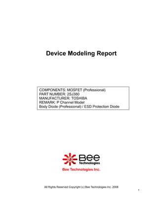
- 1. Device Modeling Report COMPONENTS: MOSFET (Professional) PART NUMBER: 2SJ380 MANUFACTURER: TOSHIBA REMARK: P Channel Model Body Diode (Professional) / ESD Protection Diode Bee Technologies Inc. All Rights Reserved Copyright (c) Bee Technologies Inc. 2008 1
- 2. Equivalent Circuit D S - - + + R3 S2 10MEG DGD R1 CGD 10M S1 + + - - S M1 G S All Rights Reserved Copyright (c) Bee Technologies Inc. 2008 2
- 3. MOSFET MODEL Pspice model Model description parameter LEVEL L Channel Length W Channel Width KP Transconductance RS Source Ohmic Resistance RD Ohmic Drain Resistance VTO Zero-bias Threshold Voltage RDS Drain-Source Shunt Resistance TOX Gate Oxide Thickness CGSO Zero-bias Gate-Source Capacitance CGDO Zero-bias Gate-Drain Capacitance CBD Zero-bias Bulk-Drain Junction Capacitance MJ Bulk Junction Grading Coefficient PB Bulk Junction Potential FC Bulk Junction Forward-bias Capacitance Coefficient RG Gate Ohmic Resistance IS Bulk Junction Saturation Current N Bulk Junction Emission Coefficient RB Bulk Series Resistance PHI Surface Inversion Potential GAMMA Body-effect Parameter DELTA Width effect on Threshold Voltage ETA Static Feedback on Threshold Voltage THETA Modility Modulation KAPPA Saturation Field Factor VMAX Maximum Drift Velocity of Carriers XJ Metallurgical Junction Depth UO Surface Mobility All Rights Reserved Copyright (c) Bee Technologies Inc. 2008 3
- 4. Transconductance Characteristic Circuit Simulation Result Comparison table gfs -Id(A) Error(%) Measurement Simulation -0.2 1.553 1.527 -1.674 -0.5 2.434 2.392 -1.726 -1 3.360 3.356 -0.119 -2 4.625 4.684 1.276 -5 7.077 7.205 1.809 -10 9.714 9.891 1.822 All Rights Reserved Copyright (c) Bee Technologies Inc. 2008 4
- 5. Vgs-Id Characteristic Circuit Simulation result -10A -1.0A -300mA 0V -1.0V -2.0V -3.0V -4.0V -5.0V -6.0V I(V3) V_V1 Evaluation circuit V3 0Vdc U1 V2 -5 2SJ380 V1 -3.5 0 All Rights Reserved Copyright (c) Bee Technologies Inc. 2008 5
- 6. Comparison Graph Circuit Simulation Result Simulation Result -VGS(V) -ID(A) Error (%) Measurement Simulation 0.05 1.654 1.712 3.507 0.1 1.734 1.768 1.961 0.2 1.830 1.846 0.874 0.5 1.992 2.002 0.502 1 2.155 2.180 1.160 2 2.375 2.435 2.526 5 2.835 2.949 4.021 10 3.415 3.546 3.836 All Rights Reserved Copyright (c) Bee Technologies Inc. 2008 6
- 7. Rds(on) Characteristic Circuit Simulation result -6.0A -4.0A -2.0A 0A 0V -0.5V -1.0V -1.5V -2.0V I(V2) V_V3 Evaluation circuit V2 0Vdc U1 V3 0Vdc 2SJ380 V1 -10 0 Simulation Result ID=-6 A, VGS=-10V Measurement Simulation Error (%) R DS (on) () 0.150 0.156 4.000 All Rights Reserved Copyright (c) Bee Technologies Inc. 2008 7
- 8. Gate Charge Characteristic Circuit Simulation result -10V -5V 0V 0 20n 40n 55n V(W1:4) Time*1mA Evaluation circuit U1 W - 2SJ380 + I2 D1 W1 Dbreak -12 IOFF = 100uA I1 TD = 0 ION = 0 TF = 10n ROFF = 1e6 PW = 200u RON = 1.0 V1 PER = 500u I1 = 0 I2 = 1m -80 TR = 10n 0 Simulation Result VDD=-80V,ID=-12A ,VGS=-10V Measurement Simulation Error (%) Qgs(nc) 7.0000 7.0606 0.866 Qgd(nc) 21.000 20.901 -0.471 Qg(nc) 55.000 55.000 0.000 All Rights Reserved Copyright (c) Bee Technologies Inc. 2008 8
- 9. Capacitance Characteristic Measurement Simulation Simulation Result Cbd(pF) VDS(V) Error(%) Measurement Simulation 0.1 950 943 -0.737 0.2 850 852 0.235 0.5 670 680 1.493 1 530 533 0.566 2 400 395 -1.250 5 260 254 -2.308 10 180 178 -1.111 20 120 123 2.500 All Rights Reserved Copyright (c) Bee Technologies Inc. 2008 9
- 10. Switching Time Characteristic Circuit Simulation result -20V -10V 0V 1.9us 2.0us 2.1us 2.2us 2.3us V(U1:G) V(U1:D)/5 Time Evaluation circuit L1 R2 50nH 8.3 U1 L2 V1 30nH V1 = 0 V2 2SJ380 V2 = -10 R4 -50 TD = 2u TR = 4n 50 TF = 4n PW = 10u PER = 30u 0 Simulation Result ID=-6A, VDD=-50V VGS=-10V Measurement Simulation Error(%) Ton(ns) 30.000 29.976 -0.080 All Rights Reserved Copyright (c) Bee Technologies Inc. 2008 10
- 11. Output Characteristic Circuit Simulation result -20A -10 V -8 V -6 V -16A -4 V -12A -3.5 V -8A -3 V -4A -2.5 V VGS=-2.0 V 0A 0V -5V -10V I(V3) V_V2 Evaluation circuit V3 0Vdc U1 V2 V1 2SJ380 -10 -2 0 All Rights Reserved Copyright (c) Bee Technologies Inc. 2008 11
- 12. BODY DIODE SPICEMODEL Forward Current Characteristic Circuit Simulation Result -10A -1.0A -300mA 0V 0.2V 0.4V 0.6V 0.8V 1.0V -I(R1) V_V1 Evaluation Circuit R1 0.01m U1 V1 0Vdc 2SJ380 0 All Rights Reserved Copyright (c) Bee Technologies Inc. 2008 12
- 13. Comparison Graph Circuit Simulation Result Simulation Result VDS(V) VDS(V) -IDR(A) %Error Measurement Simulation 0.3 0.670 0.672 0.299 0.5 0.700 0.696 -0.571 1 0.730 0.730 0.000 2 0.765 0.766 0.131 5 0.825 0.824 -0.121 10 0.885 0.885 0.000 All Rights Reserved Copyright (c) Bee Technologies Inc. 2008 13
- 14. Reverse Recovery Characteristic Circuit Simulation Result 400mA 200mA 0A -200mA -400mA 14.4us 14.8us 15.2us 15.6us 16.0us I(RL) Time Evaluation Circuit RL 50 U4 D2SJ380 V1 = -9.4 V1 V2 = 10.7 TD = 0 TR = 10n TF = 10n PW = 15u PER = 100u 0 Compare Measurement vs. Simulation Measurement Simulation Error (%) Trj(us) 152.000 152.002 0.001 Trb(us) 124.000 124.888 0.716 Trr(us) 276.000 276.890 0.322 All Rights Reserved Copyright (c) Bee Technologies Inc. 2008 14
- 15. Reverse Recovery Characteristic Reference Trj=152(ns) Trb=124(ns) Conditions:Ifwd=lrev=0.2(A),Rl=50 Example Example Relation between trj and trb Relation between trj and trb All Rights Reserved Copyright (c) Bee Technologies Inc. 2008 15
- 16. Zener Voltage Characteristic Circuit Simulation Result 10mA 5mA 0A 0V 5V 10V 15V 20V 25V 30V 35V 40V 45V 50V I(R1) V_V1 Evaluation Circuit U1 R1 R2 0.01m 1G 2SJ380 V1 0Vdc 0 All Rights Reserved Copyright (c) Bee Technologies Inc. 2008 16
- 17. Zener Voltage Characteristic Reference All Rights Reserved Copyright (c) Bee Technologies Inc. 2008 17