SlideShare una empresa de Scribd logo
1 de 11
Descargar para leer sin conexión
LR8


                                                                                                                                                                                            LR8

                                                  High Input Voltage
                                        Adjustable 3-Terminal Linear Regulator
Features                                                                                                     General Description
❏    12V to 450V input voltage range                                                                         The Supertex LR8 is a high voltage, low output current, adjustable
                                                                                                             linear regulator. It has a wide operating input voltage range of
❏    Adjustable 1.20V to 440V output regulation
                                                                                                             12V to 450V. The output voltage can be adjusted from 1.20V to
❏    5% output voltage tolerance                                                                             440V provided that the input voltage is at least 10V greater than
                                                                                                             the output voltage. The output voltage can be adjusted by means
❏    Output current limiting
                                                                                                             of two external resistors R1 and R2 as shown in the typical
❏    10µA typical ADJ current                                                                                application circuits. The LR8 regulates the voltage difference
❏    Internal junction temperature limiting                                                                  between VOUT and ADJ pins to a nominal value of 1.20V. The
                                                                                                             1.20V is amplified by the external resistor ratio R1 and R2. An
                                                                                                             internal constant bias current of typically 10µA is connected to
                                                                                                             the ADJ pin. This increases VOUT by a constant voltage of 10µA
Applications                                                                                                 times R2.

❏    Off-line SMPS startup circuits                                                                          The LR8 has current limiting and temperature limiting. The
                                                                                                             output current limit is typically 15mA and the minimum temperature
❏    Adjustable high voltage constant current source                                                         limit is 125°C. An output short circuit current will therefore be
❏    Industrial Controls                                                                                     limited to 15mA. When the junction temperature reaches its
                                                                                                             temperature limit, the output current and/or output voltage will
❏    Motor controls
                                                                                                             decrease to keep the junction temperature from exceeding its
❏    Battery chargers                                                                                        temperature limit. For SMPS start-up circuit applications, the
                                                                                                             LR8 turns off when an external voltage greater than the output
❏    Power supplies
                                                                                                             voltage of the LR8 is applied to VOUT of the LR8. To maintain
                                                                                                             stability, a bypass capacitor of 1.0µF or larger and a minimum DC
                                                                                                             output current of 500µA are required.
                                                                                                             The device is available in TO-92, TO-243AA (SOT-89), and
                                                                                                             TO-252 (D-PAK) packages.


                                         LR8 Block Diagram and Typical Application

                                                                                                    *

                                                                                                                           VOUT
                                                         VIN                          VIN       VOUT
                                                                                            ADJ
                                                                                                               R1
                                                                                 LR8
                                                                                                                                 C2
                                                               C1                                                                                  RLOAD
                                                                                                  R2


                                                     *Required for conditions where VIN is less than VOUT.


12/03/01
Supertex Inc. does not recommend the use of its products in life support applications and will not knowingly sell its products for use in such applications unless it receives an adequate "products liability
indemnification insurance agreement." Supertex does not assume responsibility for use of devices described and limits its liability to the replacement of devices determined to be defective due to
workmanship. No responsibility is assumed for possible omissions or inaccuracies. Circuitry and specifications are subject to change without notice. For the latest product specifications, refer to the
Supertex website: http://www.supertex.com. For complete liability information on all Supertex products, refer to the most current databook or to the Legal/Disclaimer page on the Supertex website.
                                                                                                     1
LR8


Ordering Information
                                Package Options                                      Product marking for TO-243AA:

             TO-92                  TO-243AA*                 TO-252                                  LR8❋

            LR8N3                      LR8N8                   LR8K4               where ❋ = 2-week alpha date code
*   Same as SOT-89. Product supplied on 2000 piece carrier tape reels.


Absolute Maximum Ratings                                                          Pin Configurations
VIN Input Voltage                                       -0.5V to +480V*
                                                                                                                                              2 (TAB)
Output Voltage Range                                     -0.5V to +470V                             TAB
                                                                                     1
                                                                                      2
Operating Ambient Temperature Range                      -40°C to +85°C                   3                                         1
                                                                                                                                         3
Operating Junction Temperature Range                   -40°C to +125°C              TO-243AA
                                                                                     (SOT-89)                      123                  TO-252
Storage Temperature Range                              -65°C to +150°C                                            TO-92                 (D-PAK)
*Voltages referenced to ADJ.
                                                                                                            VIN             VOUT             ADJ
                                                                                   TO-92                     1               2                3
                                                                                   TO-243AA                  1            2, TAB              3
                                                                                   TO-252                    1            2 (TAB)             3


Electrical Characteristics
Test conditions unless otherwise specified: -40°C < TA < 85°C.
Symbol           Parameter                                         Min    Typ     Max         Units       Test Conditions
VIN - VOUT       Input to Output Voltage Difference                12             450          V
VOUT             Overall Output Voltage Regulation                1.14    1.20    1.26         V          12V<VIN<400V, R1=2.4KΩ, R2=0
VOUT             Overall Output Voltage Regulation                 375    400     425          V          R1=2.4KΩ, R2=782KΩ
∆VOUT            Line Regulation                                          0.003   0.01        %/V         15V<VIN<400V, VOUT=5V, IOUT=0.5mA
∆VOUT            Load Regulation                                           1.4     3.0         %          VIN=15V, VOUT=5V, 0.5mA<IOUT<10mA
∆VOUT            Temperature Regulation                             -1             +1          %          VIN=15V, VOUT=5V, IOUT=10mA,
                                                                                                          -40°C<TA<85°C
IOUT             Output Current Limit                              10              20         mA          TJ < 85°C, VIN - VOUT = 10V
IOUT             Output Current Limit                                              0.5        mA          TJ > 125°C, VIN - VOUT = 450V
IOUT             Minimum Output Current                                    0.3     0.5        mA          Includes R1 and load current
IADJ             Adjust Output Current                              5      10      15          µA
C2               Minimum Output Load Capacitance                    1                          µF
DVOUT/DVIN Ripple Rejection Ratio                                  50      60                  dB         120Hz, VOUT = 5V
TLIMIT           Junction Temperature Limit                        125                         °C


                                                                             2
LR8


Thermal Characteristics
     Package              Power Dissipation                  θJC    θJA
                             @ TA=25°C                       °C/W   °C/W
       TO-92                      0.74W                      125    170
    TO-243AA                       1.6W                       15    78†
      TO-252                       2.5W                      6.25   50†
†
    Mounted on FR4 board, 25mm x 25mm x 1.57mm.
    Significant PD increase possible on ceramic substrate.


Functional Block Diagram


                                     VIN                      Pass                LR8          VOUT
                                                             Element


                                                     Overtemp &
                                                     Overcurrent           1.2V         10µA   ADJ


                                                                             3
LR8


Typical Application Circuits
                                                                     *

                                                                                      VOUT=5.0V
               VIN=15V to 450V                          V      V
                                                        IN         OUT
                                                             ADJ
                                                    LR8                      R1
                                                                             6.04KΩ
                                                                             ±1%        C2
                                       C1                                               1.0µF      RLOAD ≤16.5KΩ
                                                                   R2
                                                                   18.2KΩ
                                                                   ±1%


                                                                                  VOUT = 1.20V 1+ R2 + IADJ R2
                                                                                                  R1


              Figure 1: High Input Voltage, 5.0V Output Linear Regulator
              * Required for conditions where VIN is less than VOUT.


             VIN=15V to 450V
                                                                                                                   +
                                                            VAuxiliary
                                                                                                                   Vout1
                       LR8                                                                                          -
                  V
                      IN
                                VOUT                                                                               +
                           ADJ
                                                                                                                   Vout2
                                                  Vcc
                                                                                                                    -
                                                               FB        PWM IC


              Figure 2: SMPS Start-Up Circuit


                                                                         1µF
                                                                                                1.20V
                                              LR8                                     IOUT =
                                                                                                  R
                           +                VIN     VOUT
                                                  ADJ                    R
                 VIN = 15V
                   to 450V                                                                         Load

                            -

              Figure 3: High Voltage Adjustable Constant Current Source


                                                                    4
LR8


Typical Performance Curves
                                                                                                     Temperature Variation
                                                                                1.30


                                                                                1.25
             VIN                     VOUT=1.2V
                         LR8


                                                                 VOUT (V)
                                                                                1.20


                    ADJ
                                                                                1.15
  12V                                     2.4KΩ          1.0µF

                                                                                1.10


                                                                                1.05


                                                                                1.00
                                                                                    -50    -25        0       25    50       75       100   125

                                                                                                          T(junction) (°C)


                                                                                                      Adjustment Current
                                                                                 12


                                                                                 11
             VIN                     VOUT=1.2V
                                                                    IADJ (µA)


                                                                                 10
                         LR8
                                                                                             VIN = 400V

12V,                ADJ                                                           9                                 VIN = 12V

200V,                                         2.4KΩ      1.0µF
400V
                           I                                                      8
                           ADJ

                                                                                             VIN = 200V
                                                                                  7


                                                                                  6
                                                                                   -50     -25        0       25    50       75       100   125
                                                                                                          T(junction) (°C)


                                                                                                       Load Regulation
                                                                                 5.2


        V                  V     =5.0V        IOUT
        IN                     OUT
                   LR8
                                                                                 5.1
                                                                 VOUT (V)


              ADJ                    6.04KΩ
                                       ±1%
                                                 1.0µF                           5.0
25V
                                                         RLOAD
                     18.2KΩ
                      ±1%
                                                                                 4.9


                                                                                 4.8
                                                                                       0         2           4        6           8         10

                                                                                                            IOUT (mA)

                                                                 5
LR8


Typical Performance Curves
                                                                                                                        VOUT vs. VIN
                                                                                                         6


              VIN                VOUT=5.0V                                                               5
                          LR8
                                                                                                         4


                                                                      VOUT (V)
                     ADJ              6.04KΩ
                                        ±1%

0V to 50V                                             1.0µF   1KΩ                                        3

                            18.2KΩ
                             ±1%                                                                         2


                                                                                                         1


                                                                                                         0
                                                                                                              0   10      20      30      40   50

                                                                                                                           VIN (V)


                                                                                                                       Ripple Rejection
                                                                                                        -65
                                                                          Ripple Rejection Ratio (dB)


            VIN                 VOUT =5.0V     IOUT                                                     -64
                      LR8

                    ADJ              6.04KΩ                                                             -63
20VP-P
                                       ±1%
@ 60Hz
                                                  1.0µF
                                                              RLOAD                                     -62
  65V                      18.2KΩ
                            ±1%
                                                                                                        -61


                                                                                                        -60
                                                                                                              0   2       4          6    8    10

                                                                                                                         IOUT (mA)


                                                                      6
LR8


Typical Performance Curves
                            Load Transient Response

             VIN                     VOUT=5.0V
                        LR8                                                                      Closed
                                                                                                  SW
                   ADJ                       6.04KΩ                                       SW     Open
                                               ±1%

25V                                                           1.0µF          10KΩ
                             18.2KΩ                                                     523 Ω     Vout
                              ±1%


                                                                                                          Load Transient Response

                            Line Transient Response
400V                                                                                               400V
                      VIN                       VOUT
VIN                                LR8
0V
                              ADJ                       6.04KΩ                                     Vin
                                                          ±1%
                                                                            1.0µF       10KΩ
                                                                                          5.0V
                                        18.2KΩ                                                      0V
                                         ±1%


                                                                                                  Vout
                                                                                                   0V


                                                                                                           Line Transient Response


      400V                                                                                        400V


      Vin                                                                                        Vin


         0V                                                                                        0V

        5.0V                                                                                       5.0V
      Vout                                                                                       Vout
          0V                                                                                       0V


                             Line Power Up Transient                                                      Line Power Down Transient


                                                                                                                                         12/03/01rev.2

                                                                                                          1235 Bordeaux Drive, Sunnyvale, CA 94089
                                                                                                           TEL: (408) 744-0100 • FAX: (408) 222-4895
©2001 Supertex Inc. All rights reserved. Unauthorized use or reproduction prohibited.
                                                                                           7                                       www.supertex.com
LR8 LR8

                                                                                                                 Application Note
                                                                                                                          AN-H40

                                High Voltage Linear Regulators and
                               Constant Current Sources Using LR8
                                                by Scott Lynch, Senior Applications Engineer


Introduction                                                                      Operation
The LR8 is a high voltage 3-terminal adjustable linear regulator.                 Except for it’s higher voltage rating, the LR8 operates like any
Intended for operation directly off rectified AC mains, the LR8                   other 3-terminal adjustable linear regulator.
operates at input voltages up to 450 volts, making it compatible
                                                                                  A simple resistive divider sets the output voltage while a capacitor
with line voltages up to 240 VAC. It’s output voltage adjustability
                                                                                  at the output improves transient response and ensures regulator
assures that it can be used in most any application. The LR8 is
                                                                                  stability. When applicable, an input capacitor is required to
ideally suited for low power off-line DC power supplies and
                                                                                  provide energy storage for rectified AC.
SMPS start-up circuits.
                                                                                  Keeping in mind that the LR8 requires at least a 10V difference
Available in a leaded TO-92 package and a surface mount
                                                                                  between input and output for proper operation, the minimum
SOT-89 and D-PAK package, it is ideal for applications where
                                                                                  value for CIN is:
space is at a premium.
Relevant specifications are shown in the table below.                                                                         t
                                                                                                CIN > I LOAD
                                                                                                                VIN ( pk ) − VOUT − 10V
LR8 Specifications                                                                             where        ILOAD = Load current
 Input Voltage Range                       (VOUT +10V) to 450V                                              t       = Time between peaks of input
 Output Voltage Range                        1.2V to (VIN - 10V)                                                      waveform
                                                                                                            VIN(pk) = Peak input voltage
 Output Voltage Accuracy                                      ±5%                                           VOUT = Output voltage
 Power Dissipation               TO-92:            0.74W
                                 TO-243AA (SOT-89): 1.6W
                                 TO-252 (D-PAK):    2.5W                          Note that the LR8 requires a minimum of 0.5mA load current for
                                                                                  proper operation. The current through the resistive divider may
 Output Current                                      0.5 to 10mA
                                                                                  be included as part of the minimum load.
 Load Regulation                                                3%
 Line Regulation                                         0.01%/V
 Supply Rejection                            60dB typ @120Hz


                               LR8 Block Diagram and Typical Application
                                        Needed for protection should V OUT exceed V IN

                                                                                                                       R 
                                                                                                        VOUT = 1.2 v1 + 2  + 10µA • R2
                                                                                                                       R1 
                                VIN           Pass                 LR8                   VOUT
                Supply                       Element                                                                   Load


                                                                                                       R1
                                          Overtemp &
                                          Overcurrent       1.2V           10µA          ADJ
                         CIN                                                                                      COUT
                                                                                                                  ≥ 1µF

                                                                                                       R2


                                                                            8
LR8


Constant Current Operation
The LR8 may be configured to provide a constant current output. The current is independent of both supply voltage and load impedance.
Constant current operation finds application in driving LEDs and trickle-charging NiCad batteries, as shown below. The trickle charger is
for applications that require battery backup (i.e. no cycling), such as emergency lights.


         Constant Current LED Driver                                           NiCad Battery Trickle Charger

                                                      R                                                                          R
                         LR8                                                                        LR8

         15V
          to                                                                         15V
        450V                                                                          to
                                                                                    450V


Start-up Circuit
The schematic below depicts a simplified off-line switching power supply using the LR8 for start-up. When VBOOT rises above the LR8’s
output voltage, the LR8 goes into standby mode, consuming very little current. All current is then supplied from the bootstrap circuit rather
than from the high voltage source, increasing overall efficiency.
The output voltage of the LR8 should be set high enough above the minimum operating voltage of the PWM controller, yet low enough
to ensure the bootstrap circuit takes over after start-up.
With 240VAC input, instantaneous power dissipation can reach 3.4W (340VDC * 10mA). This level exceeds the LR8’s rating, but exists
for only as long as it takes for the supply to bootstrap. Thermal mass will prevent die temperature from rising quickly. If boot time is short,
die temperatures will not reach the overtemperature protection trip point. It is advisable to mount the LR8 on 2 oz. copper with an area
of at least 2.5 square centimeters.


                          Startup Current for Off-line Switching Power Supply

                                                                                                    bootstrap
                                                                                                     winding
                                                                            VBOOT


                                                                              D1
                                  VIN                               VOUT                 PWM
                                                  LR8
                                                                                       Controller
  AC                                                         R1
Mains

                                         CIN                                 COUT
                                                             R2


                                                                       9
LR8


Comparison with Discrete Startup Implementations
The LR8 provides several advantages when compared with discretely implemented start-up circuits.


   Zener Implementation                 Transistor Implementation                                LR8 Implementation
  VIN                          VOUT      VIN                   VOUT
                                                                                         VIN           LR8                   VOUT


    Disadvantages
    • Continues to draw current from high voltage source after
      supply has bootstrapped, resulting in inefficiencies                     Advantages
    • Bias must be set for minimum input voltage, resulting in                 • LR8 goes into standby mode after supply has
      high current drain at high input voltages                                  bootstrapped, drawing no current from high voltage
    • Poor regulation                                                            input
    • No current limit                                                         • Good regulation
    • No overtemperature protection                                            • Built-in current limiting
    • In the Zener implementation, requires large power resistor               • Overtemperature protection
      and Zener


Exceeding LR8’s Current Limit for Startup Applications
The LR8 has a built-in current limit of 10mA minimum. If the current drawn by the PWM controller exceeds this limit, the LR8 may still be
used. To do this, the LR8’s output capacitor supplies a portion of the current until the power supply can bootstrap itself and the LR8 is no
longer needed. The following figure graphically illustrates how this is accomplished.
Most PWM controllers have an undervoltage lockout (UVL) circuit or programmable start/stop voltages. When the voltage supplied to the
PWM controller reaches the turn-on threshold, the controller begins operating and consuming current. If current exceeds the current limit
for the LR8, the voltage at VOUT begins to decay. With a large enough capacitor, the supply will bootstrap before voltage decays to the turn-
off threshold.


                                                                      1    Input voltage is applied. The LR8 begins operating (in current
        VIN     1                                                          limiting mode since COUT appears as a short). VOUT begins to
                                                                           rise as COUT charges. The PWM controller draws a small
                                                                           amount of current.
                    VOUT                  4

                                                                      2    The output voltage of the LR8 reaches the PWM controller’s
                                                     VHYS                  turn-on threshold. Controller begins operating, drawing current.
                                                                           Bootstrap voltage begins climbing while VOUT decays since
                                                                           current drawn by the controller exceeds the LR8’s current limit.
         VBOOT                        tBOOT
                           2      3
                                                                      3    Bootstrap voltage reaches the level of the LR8’s output and
               IPWM                                                        takes over. LR8 current drops to zero.

                                      10mA
        ILR8
                                                                      4    Power supply reaches steady-state operation.
                                                   0mA


                                                                      10
LR8

The minimum capacitance required for given boot-up time is
given by the following equation:

                            I PWM − I LIM
            COUT > t BOOT
                                VHYS

   where    COUT    =   Capacitor at LR8 output
            tBOOT   =   Time required for supply to bootstrap
            IPWM    =   Current used by PWM controller
            ILIM    =   LR8 current limit (10mA min)
            VHYS    =   PWM controller UVL hysteresis


Remember that this equation is valid only when PWM current
exceeds the LR8’s current limit.


                                                                                                                 11/30/01rev.1

                                                                     1235 Bordeaux Drive, Sunnyvale, CA 94089
                                                                     TEL: (408) 744-0100 • FAX: (408) 222-4895
                                                                11   www.supertex.com

Más contenido relacionado

Similar a Datasheet of LR8

Relay driver basic
Relay driver basicRelay driver basic
Relay driver basicBien Morfe
 
Design and fabrication of over voltage relay
Design and fabrication of over voltage relay Design and fabrication of over voltage relay
Design and fabrication of over voltage relay Prem Kumar
 
Original High Performance Off-Line Controller IC ACT30 CT30 30 New Active-Semi
Original High Performance Off-Line Controller IC ACT30 CT30 30 New Active-SemiOriginal High Performance Off-Line Controller IC ACT30 CT30 30 New Active-Semi
Original High Performance Off-Line Controller IC ACT30 CT30 30 New Active-SemiAUTHELECTRONIC
 
Integrated circuit
Integrated circuitIntegrated circuit
Integrated circuitddsshukla
 
Digital potentiometer ds1804 010+
Digital potentiometer ds1804 010+Digital potentiometer ds1804 010+
Digital potentiometer ds1804 010+robertoestrella
 
Analog IC Application
Analog IC ApplicationAnalog IC Application
Analog IC ApplicationTamilarasan N
 
Integrated-Circuit-Regulator-1.pptx
Integrated-Circuit-Regulator-1.pptxIntegrated-Circuit-Regulator-1.pptx
Integrated-Circuit-Regulator-1.pptxElmar7
 
One Touch Electrical Appliances Control Using Microcontroller 89C51
One Touch Electrical Appliances Control Using Microcontroller 89C51One Touch Electrical Appliances Control Using Microcontroller 89C51
One Touch Electrical Appliances Control Using Microcontroller 89C51Pawan Bahuguna
 
DVD Player Multiple Output Di115 2
DVD Player Multiple Output Di115 2DVD Player Multiple Output Di115 2
DVD Player Multiple Output Di115 2gueste54184
 
LT3755 - High Side Sense LED Controller for High Current LED Applications
LT3755 - High Side Sense LED Controller for  High Current LED ApplicationsLT3755 - High Side Sense LED Controller for  High Current LED Applications
LT3755 - High Side Sense LED Controller for High Current LED ApplicationsPremier Farnell
 
LT3496 - Triple Output LED Driver
LT3496 - Triple Output LED DriverLT3496 - Triple Output LED Driver
LT3496 - Triple Output LED DriverPremier Farnell
 
Advanced motions controls 20a14
Advanced motions controls 20a14Advanced motions controls 20a14
Advanced motions controls 20a14Electromate
 
Basic Protection of transformer using microcontroller based relay
Basic Protection of transformer using microcontroller based relayBasic Protection of transformer using microcontroller based relay
Basic Protection of transformer using microcontroller based relaySatish Dharpure
 
Advanced motion controls 120a5
Advanced motion controls 120a5Advanced motion controls 120a5
Advanced motion controls 120a5Electromate
 
An Overview of the Power Over Ethernet and PWM Controller: LM5072
An Overview of the Power Over Ethernet and PWM Controller: LM5072An Overview of the Power Over Ethernet and PWM Controller: LM5072
An Overview of the Power Over Ethernet and PWM Controller: LM5072Premier Farnell
 

Similar a Datasheet of LR8 (20)

Relay driver basic
Relay driver basicRelay driver basic
Relay driver basic
 
Design and fabrication of over voltage relay
Design and fabrication of over voltage relay Design and fabrication of over voltage relay
Design and fabrication of over voltage relay
 
Pr adee (2)
Pr adee (2)Pr adee (2)
Pr adee (2)
 
Original High Performance Off-Line Controller IC ACT30 CT30 30 New Active-Semi
Original High Performance Off-Line Controller IC ACT30 CT30 30 New Active-SemiOriginal High Performance Off-Line Controller IC ACT30 CT30 30 New Active-Semi
Original High Performance Off-Line Controller IC ACT30 CT30 30 New Active-Semi
 
Integrated circuit
Integrated circuitIntegrated circuit
Integrated circuit
 
Wk105 (1)
Wk105 (1)Wk105 (1)
Wk105 (1)
 
Digital potentiometer ds1804 010+
Digital potentiometer ds1804 010+Digital potentiometer ds1804 010+
Digital potentiometer ds1804 010+
 
Analog IC Application
Analog IC ApplicationAnalog IC Application
Analog IC Application
 
Integrated-Circuit-Regulator-1.pptx
Integrated-Circuit-Regulator-1.pptxIntegrated-Circuit-Regulator-1.pptx
Integrated-Circuit-Regulator-1.pptx
 
Ad598
Ad598Ad598
Ad598
 
One Touch Electrical Appliances Control Using Microcontroller 89C51
One Touch Electrical Appliances Control Using Microcontroller 89C51One Touch Electrical Appliances Control Using Microcontroller 89C51
One Touch Electrical Appliances Control Using Microcontroller 89C51
 
DVD Player Multiple Output Di115 2
DVD Player Multiple Output Di115 2DVD Player Multiple Output Di115 2
DVD Player Multiple Output Di115 2
 
LT3755 - High Side Sense LED Controller for High Current LED Applications
LT3755 - High Side Sense LED Controller for  High Current LED ApplicationsLT3755 - High Side Sense LED Controller for  High Current LED Applications
LT3755 - High Side Sense LED Controller for High Current LED Applications
 
LT3496 - Triple Output LED Driver
LT3496 - Triple Output LED DriverLT3496 - Triple Output LED Driver
LT3496 - Triple Output LED Driver
 
Mp8126 r1.03 1384507
Mp8126 r1.03 1384507Mp8126 r1.03 1384507
Mp8126 r1.03 1384507
 
Advanced motions controls 20a14
Advanced motions controls 20a14Advanced motions controls 20a14
Advanced motions controls 20a14
 
lm3914.pdf
lm3914.pdflm3914.pdf
lm3914.pdf
 
Basic Protection of transformer using microcontroller based relay
Basic Protection of transformer using microcontroller based relayBasic Protection of transformer using microcontroller based relay
Basic Protection of transformer using microcontroller based relay
 
Advanced motion controls 120a5
Advanced motion controls 120a5Advanced motion controls 120a5
Advanced motion controls 120a5
 
An Overview of the Power Over Ethernet and PWM Controller: LM5072
An Overview of the Power Over Ethernet and PWM Controller: LM5072An Overview of the Power Over Ethernet and PWM Controller: LM5072
An Overview of the Power Over Ethernet and PWM Controller: LM5072
 

Más de Tsuyoshi Horigome

Update 46 models(Solar Cell) in SPICE PARK(MAY2024)
Update 46 models(Solar Cell) in SPICE PARK(MAY2024)Update 46 models(Solar Cell) in SPICE PARK(MAY2024)
Update 46 models(Solar Cell) in SPICE PARK(MAY2024)Tsuyoshi Horigome
 
SPICE PARK APR2024 ( 6,793 SPICE Models )
SPICE PARK APR2024 ( 6,793 SPICE Models )SPICE PARK APR2024 ( 6,793 SPICE Models )
SPICE PARK APR2024 ( 6,793 SPICE Models )Tsuyoshi Horigome
 
Update 22 models(Schottky Rectifier ) in SPICE PARK(APR2024)
Update 22 models(Schottky Rectifier ) in SPICE PARK(APR2024)Update 22 models(Schottky Rectifier ) in SPICE PARK(APR2024)
Update 22 models(Schottky Rectifier ) in SPICE PARK(APR2024)Tsuyoshi Horigome
 
SPICE PARK APR2024 ( 6,747 SPICE Models )
SPICE PARK APR2024 ( 6,747 SPICE Models )SPICE PARK APR2024 ( 6,747 SPICE Models )
SPICE PARK APR2024 ( 6,747 SPICE Models )Tsuyoshi Horigome
 
Update 31 models(Diode/General ) in SPICE PARK(MAR2024)
Update 31 models(Diode/General ) in SPICE PARK(MAR2024)Update 31 models(Diode/General ) in SPICE PARK(MAR2024)
Update 31 models(Diode/General ) in SPICE PARK(MAR2024)Tsuyoshi Horigome
 
SPICE PARK MAR2024 ( 6,725 SPICE Models )
SPICE PARK MAR2024 ( 6,725 SPICE Models )SPICE PARK MAR2024 ( 6,725 SPICE Models )
SPICE PARK MAR2024 ( 6,725 SPICE Models )Tsuyoshi Horigome
 
Update 29 models(Solar cell) in SPICE PARK(FEB2024)
Update 29 models(Solar cell) in SPICE PARK(FEB2024)Update 29 models(Solar cell) in SPICE PARK(FEB2024)
Update 29 models(Solar cell) in SPICE PARK(FEB2024)Tsuyoshi Horigome
 
SPICE PARK FEB2024 ( 6,694 SPICE Models )
SPICE PARK FEB2024 ( 6,694 SPICE Models )SPICE PARK FEB2024 ( 6,694 SPICE Models )
SPICE PARK FEB2024 ( 6,694 SPICE Models )Tsuyoshi Horigome
 
Circuit simulation using LTspice(Case study)
Circuit simulation using LTspice(Case study)Circuit simulation using LTspice(Case study)
Circuit simulation using LTspice(Case study)Tsuyoshi Horigome
 
Mindmap of Semiconductor sales business(15FEB2024)
Mindmap of Semiconductor sales business(15FEB2024)Mindmap of Semiconductor sales business(15FEB2024)
Mindmap of Semiconductor sales business(15FEB2024)Tsuyoshi Horigome
 
2-STAGE COCKCROFT-WALTON [SCHEMATIC] using LTspice
2-STAGE COCKCROFT-WALTON [SCHEMATIC] using LTspice2-STAGE COCKCROFT-WALTON [SCHEMATIC] using LTspice
2-STAGE COCKCROFT-WALTON [SCHEMATIC] using LTspiceTsuyoshi Horigome
 
PSpice simulation of power supply for TI is Error
PSpice simulation of power supply  for TI is ErrorPSpice simulation of power supply  for TI is Error
PSpice simulation of power supply for TI is ErrorTsuyoshi Horigome
 
IGBT Simulation of Results from Rgext or Rgint
IGBT Simulation of Results from Rgext or RgintIGBT Simulation of Results from Rgext or Rgint
IGBT Simulation of Results from Rgext or RgintTsuyoshi Horigome
 
Electronic component sales method centered on alternative proposals
Electronic component sales method centered on alternative proposalsElectronic component sales method centered on alternative proposals
Electronic component sales method centered on alternative proposalsTsuyoshi Horigome
 
Electronic component sales method focused on new hires
Electronic component sales method focused on new hiresElectronic component sales method focused on new hires
Electronic component sales method focused on new hiresTsuyoshi Horigome
 
Mindmap(electronics parts sales visions)
Mindmap(electronics parts sales visions)Mindmap(electronics parts sales visions)
Mindmap(electronics parts sales visions)Tsuyoshi Horigome
 
Chat GPTによる伝達関数の導出
Chat GPTによる伝達関数の導出Chat GPTによる伝達関数の導出
Chat GPTによる伝達関数の導出Tsuyoshi Horigome
 
伝達関数の理解(Chatgpt)
伝達関数の理解(Chatgpt)伝達関数の理解(Chatgpt)
伝達関数の理解(Chatgpt)Tsuyoshi Horigome
 
DXセミナー(2024年1月17日開催)のメモ
DXセミナー(2024年1月17日開催)のメモDXセミナー(2024年1月17日開催)のメモ
DXセミナー(2024年1月17日開催)のメモTsuyoshi Horigome
 
0Ω抵抗を評価ボードで採用する理由は何ですか?
0Ω抵抗を評価ボードで採用する理由は何ですか?0Ω抵抗を評価ボードで採用する理由は何ですか?
0Ω抵抗を評価ボードで採用する理由は何ですか?Tsuyoshi Horigome
 

Más de Tsuyoshi Horigome (20)

Update 46 models(Solar Cell) in SPICE PARK(MAY2024)
Update 46 models(Solar Cell) in SPICE PARK(MAY2024)Update 46 models(Solar Cell) in SPICE PARK(MAY2024)
Update 46 models(Solar Cell) in SPICE PARK(MAY2024)
 
SPICE PARK APR2024 ( 6,793 SPICE Models )
SPICE PARK APR2024 ( 6,793 SPICE Models )SPICE PARK APR2024 ( 6,793 SPICE Models )
SPICE PARK APR2024 ( 6,793 SPICE Models )
 
Update 22 models(Schottky Rectifier ) in SPICE PARK(APR2024)
Update 22 models(Schottky Rectifier ) in SPICE PARK(APR2024)Update 22 models(Schottky Rectifier ) in SPICE PARK(APR2024)
Update 22 models(Schottky Rectifier ) in SPICE PARK(APR2024)
 
SPICE PARK APR2024 ( 6,747 SPICE Models )
SPICE PARK APR2024 ( 6,747 SPICE Models )SPICE PARK APR2024 ( 6,747 SPICE Models )
SPICE PARK APR2024 ( 6,747 SPICE Models )
 
Update 31 models(Diode/General ) in SPICE PARK(MAR2024)
Update 31 models(Diode/General ) in SPICE PARK(MAR2024)Update 31 models(Diode/General ) in SPICE PARK(MAR2024)
Update 31 models(Diode/General ) in SPICE PARK(MAR2024)
 
SPICE PARK MAR2024 ( 6,725 SPICE Models )
SPICE PARK MAR2024 ( 6,725 SPICE Models )SPICE PARK MAR2024 ( 6,725 SPICE Models )
SPICE PARK MAR2024 ( 6,725 SPICE Models )
 
Update 29 models(Solar cell) in SPICE PARK(FEB2024)
Update 29 models(Solar cell) in SPICE PARK(FEB2024)Update 29 models(Solar cell) in SPICE PARK(FEB2024)
Update 29 models(Solar cell) in SPICE PARK(FEB2024)
 
SPICE PARK FEB2024 ( 6,694 SPICE Models )
SPICE PARK FEB2024 ( 6,694 SPICE Models )SPICE PARK FEB2024 ( 6,694 SPICE Models )
SPICE PARK FEB2024 ( 6,694 SPICE Models )
 
Circuit simulation using LTspice(Case study)
Circuit simulation using LTspice(Case study)Circuit simulation using LTspice(Case study)
Circuit simulation using LTspice(Case study)
 
Mindmap of Semiconductor sales business(15FEB2024)
Mindmap of Semiconductor sales business(15FEB2024)Mindmap of Semiconductor sales business(15FEB2024)
Mindmap of Semiconductor sales business(15FEB2024)
 
2-STAGE COCKCROFT-WALTON [SCHEMATIC] using LTspice
2-STAGE COCKCROFT-WALTON [SCHEMATIC] using LTspice2-STAGE COCKCROFT-WALTON [SCHEMATIC] using LTspice
2-STAGE COCKCROFT-WALTON [SCHEMATIC] using LTspice
 
PSpice simulation of power supply for TI is Error
PSpice simulation of power supply  for TI is ErrorPSpice simulation of power supply  for TI is Error
PSpice simulation of power supply for TI is Error
 
IGBT Simulation of Results from Rgext or Rgint
IGBT Simulation of Results from Rgext or RgintIGBT Simulation of Results from Rgext or Rgint
IGBT Simulation of Results from Rgext or Rgint
 
Electronic component sales method centered on alternative proposals
Electronic component sales method centered on alternative proposalsElectronic component sales method centered on alternative proposals
Electronic component sales method centered on alternative proposals
 
Electronic component sales method focused on new hires
Electronic component sales method focused on new hiresElectronic component sales method focused on new hires
Electronic component sales method focused on new hires
 
Mindmap(electronics parts sales visions)
Mindmap(electronics parts sales visions)Mindmap(electronics parts sales visions)
Mindmap(electronics parts sales visions)
 
Chat GPTによる伝達関数の導出
Chat GPTによる伝達関数の導出Chat GPTによる伝達関数の導出
Chat GPTによる伝達関数の導出
 
伝達関数の理解(Chatgpt)
伝達関数の理解(Chatgpt)伝達関数の理解(Chatgpt)
伝達関数の理解(Chatgpt)
 
DXセミナー(2024年1月17日開催)のメモ
DXセミナー(2024年1月17日開催)のメモDXセミナー(2024年1月17日開催)のメモ
DXセミナー(2024年1月17日開催)のメモ
 
0Ω抵抗を評価ボードで採用する理由は何ですか?
0Ω抵抗を評価ボードで採用する理由は何ですか?0Ω抵抗を評価ボードで採用する理由は何ですか?
0Ω抵抗を評価ボードで採用する理由は何ですか?
 

Último

🐬 The future of MySQL is Postgres 🐘
🐬  The future of MySQL is Postgres   🐘🐬  The future of MySQL is Postgres   🐘
🐬 The future of MySQL is Postgres 🐘RTylerCroy
 
Handwritten Text Recognition for manuscripts and early printed texts
Handwritten Text Recognition for manuscripts and early printed textsHandwritten Text Recognition for manuscripts and early printed texts
Handwritten Text Recognition for manuscripts and early printed textsMaria Levchenko
 
FULL ENJOY 🔝 8264348440 🔝 Call Girls in Diplomatic Enclave | Delhi
FULL ENJOY 🔝 8264348440 🔝 Call Girls in Diplomatic Enclave | DelhiFULL ENJOY 🔝 8264348440 🔝 Call Girls in Diplomatic Enclave | Delhi
FULL ENJOY 🔝 8264348440 🔝 Call Girls in Diplomatic Enclave | Delhisoniya singh
 
Finology Group – Insurtech Innovation Award 2024
Finology Group – Insurtech Innovation Award 2024Finology Group – Insurtech Innovation Award 2024
Finology Group – Insurtech Innovation Award 2024The Digital Insurer
 
#StandardsGoals for 2024: What’s new for BISAC - Tech Forum 2024
#StandardsGoals for 2024: What’s new for BISAC - Tech Forum 2024#StandardsGoals for 2024: What’s new for BISAC - Tech Forum 2024
#StandardsGoals for 2024: What’s new for BISAC - Tech Forum 2024BookNet Canada
 
SQL Database Design For Developers at php[tek] 2024
SQL Database Design For Developers at php[tek] 2024SQL Database Design For Developers at php[tek] 2024
SQL Database Design For Developers at php[tek] 2024Scott Keck-Warren
 
Salesforce Community Group Quito, Salesforce 101
Salesforce Community Group Quito, Salesforce 101Salesforce Community Group Quito, Salesforce 101
Salesforce Community Group Quito, Salesforce 101Paola De la Torre
 
The Codex of Business Writing Software for Real-World Solutions 2.pptx
The Codex of Business Writing Software for Real-World Solutions 2.pptxThe Codex of Business Writing Software for Real-World Solutions 2.pptx
The Codex of Business Writing Software for Real-World Solutions 2.pptxMalak Abu Hammad
 
Tech-Forward - Achieving Business Readiness For Copilot in Microsoft 365
Tech-Forward - Achieving Business Readiness For Copilot in Microsoft 365Tech-Forward - Achieving Business Readiness For Copilot in Microsoft 365
Tech-Forward - Achieving Business Readiness For Copilot in Microsoft 3652toLead Limited
 
How to convert PDF to text with Nanonets
How to convert PDF to text with NanonetsHow to convert PDF to text with Nanonets
How to convert PDF to text with Nanonetsnaman860154
 
From Event to Action: Accelerate Your Decision Making with Real-Time Automation
From Event to Action: Accelerate Your Decision Making with Real-Time AutomationFrom Event to Action: Accelerate Your Decision Making with Real-Time Automation
From Event to Action: Accelerate Your Decision Making with Real-Time AutomationSafe Software
 
Histor y of HAM Radio presentation slide
Histor y of HAM Radio presentation slideHistor y of HAM Radio presentation slide
Histor y of HAM Radio presentation slidevu2urc
 
Slack Application Development 101 Slides
Slack Application Development 101 SlidesSlack Application Development 101 Slides
Slack Application Development 101 Slidespraypatel2
 
IAC 2024 - IA Fast Track to Search Focused AI Solutions
IAC 2024 - IA Fast Track to Search Focused AI SolutionsIAC 2024 - IA Fast Track to Search Focused AI Solutions
IAC 2024 - IA Fast Track to Search Focused AI SolutionsEnterprise Knowledge
 
GenCyber Cyber Security Day Presentation
GenCyber Cyber Security Day PresentationGenCyber Cyber Security Day Presentation
GenCyber Cyber Security Day PresentationMichael W. Hawkins
 
08448380779 Call Girls In Civil Lines Women Seeking Men
08448380779 Call Girls In Civil Lines Women Seeking Men08448380779 Call Girls In Civil Lines Women Seeking Men
08448380779 Call Girls In Civil Lines Women Seeking MenDelhi Call girls
 
Unblocking The Main Thread Solving ANRs and Frozen Frames
Unblocking The Main Thread Solving ANRs and Frozen FramesUnblocking The Main Thread Solving ANRs and Frozen Frames
Unblocking The Main Thread Solving ANRs and Frozen FramesSinan KOZAK
 
Strategies for Unlocking Knowledge Management in Microsoft 365 in the Copilot...
Strategies for Unlocking Knowledge Management in Microsoft 365 in the Copilot...Strategies for Unlocking Knowledge Management in Microsoft 365 in the Copilot...
Strategies for Unlocking Knowledge Management in Microsoft 365 in the Copilot...Drew Madelung
 
08448380779 Call Girls In Friends Colony Women Seeking Men
08448380779 Call Girls In Friends Colony Women Seeking Men08448380779 Call Girls In Friends Colony Women Seeking Men
08448380779 Call Girls In Friends Colony Women Seeking MenDelhi Call girls
 
[2024]Digital Global Overview Report 2024 Meltwater.pdf
[2024]Digital Global Overview Report 2024 Meltwater.pdf[2024]Digital Global Overview Report 2024 Meltwater.pdf
[2024]Digital Global Overview Report 2024 Meltwater.pdfhans926745
 

Último (20)

🐬 The future of MySQL is Postgres 🐘
🐬  The future of MySQL is Postgres   🐘🐬  The future of MySQL is Postgres   🐘
🐬 The future of MySQL is Postgres 🐘
 
Handwritten Text Recognition for manuscripts and early printed texts
Handwritten Text Recognition for manuscripts and early printed textsHandwritten Text Recognition for manuscripts and early printed texts
Handwritten Text Recognition for manuscripts and early printed texts
 
FULL ENJOY 🔝 8264348440 🔝 Call Girls in Diplomatic Enclave | Delhi
FULL ENJOY 🔝 8264348440 🔝 Call Girls in Diplomatic Enclave | DelhiFULL ENJOY 🔝 8264348440 🔝 Call Girls in Diplomatic Enclave | Delhi
FULL ENJOY 🔝 8264348440 🔝 Call Girls in Diplomatic Enclave | Delhi
 
Finology Group – Insurtech Innovation Award 2024
Finology Group – Insurtech Innovation Award 2024Finology Group – Insurtech Innovation Award 2024
Finology Group – Insurtech Innovation Award 2024
 
#StandardsGoals for 2024: What’s new for BISAC - Tech Forum 2024
#StandardsGoals for 2024: What’s new for BISAC - Tech Forum 2024#StandardsGoals for 2024: What’s new for BISAC - Tech Forum 2024
#StandardsGoals for 2024: What’s new for BISAC - Tech Forum 2024
 
SQL Database Design For Developers at php[tek] 2024
SQL Database Design For Developers at php[tek] 2024SQL Database Design For Developers at php[tek] 2024
SQL Database Design For Developers at php[tek] 2024
 
Salesforce Community Group Quito, Salesforce 101
Salesforce Community Group Quito, Salesforce 101Salesforce Community Group Quito, Salesforce 101
Salesforce Community Group Quito, Salesforce 101
 
The Codex of Business Writing Software for Real-World Solutions 2.pptx
The Codex of Business Writing Software for Real-World Solutions 2.pptxThe Codex of Business Writing Software for Real-World Solutions 2.pptx
The Codex of Business Writing Software for Real-World Solutions 2.pptx
 
Tech-Forward - Achieving Business Readiness For Copilot in Microsoft 365
Tech-Forward - Achieving Business Readiness For Copilot in Microsoft 365Tech-Forward - Achieving Business Readiness For Copilot in Microsoft 365
Tech-Forward - Achieving Business Readiness For Copilot in Microsoft 365
 
How to convert PDF to text with Nanonets
How to convert PDF to text with NanonetsHow to convert PDF to text with Nanonets
How to convert PDF to text with Nanonets
 
From Event to Action: Accelerate Your Decision Making with Real-Time Automation
From Event to Action: Accelerate Your Decision Making with Real-Time AutomationFrom Event to Action: Accelerate Your Decision Making with Real-Time Automation
From Event to Action: Accelerate Your Decision Making with Real-Time Automation
 
Histor y of HAM Radio presentation slide
Histor y of HAM Radio presentation slideHistor y of HAM Radio presentation slide
Histor y of HAM Radio presentation slide
 
Slack Application Development 101 Slides
Slack Application Development 101 SlidesSlack Application Development 101 Slides
Slack Application Development 101 Slides
 
IAC 2024 - IA Fast Track to Search Focused AI Solutions
IAC 2024 - IA Fast Track to Search Focused AI SolutionsIAC 2024 - IA Fast Track to Search Focused AI Solutions
IAC 2024 - IA Fast Track to Search Focused AI Solutions
 
GenCyber Cyber Security Day Presentation
GenCyber Cyber Security Day PresentationGenCyber Cyber Security Day Presentation
GenCyber Cyber Security Day Presentation
 
08448380779 Call Girls In Civil Lines Women Seeking Men
08448380779 Call Girls In Civil Lines Women Seeking Men08448380779 Call Girls In Civil Lines Women Seeking Men
08448380779 Call Girls In Civil Lines Women Seeking Men
 
Unblocking The Main Thread Solving ANRs and Frozen Frames
Unblocking The Main Thread Solving ANRs and Frozen FramesUnblocking The Main Thread Solving ANRs and Frozen Frames
Unblocking The Main Thread Solving ANRs and Frozen Frames
 
Strategies for Unlocking Knowledge Management in Microsoft 365 in the Copilot...
Strategies for Unlocking Knowledge Management in Microsoft 365 in the Copilot...Strategies for Unlocking Knowledge Management in Microsoft 365 in the Copilot...
Strategies for Unlocking Knowledge Management in Microsoft 365 in the Copilot...
 
08448380779 Call Girls In Friends Colony Women Seeking Men
08448380779 Call Girls In Friends Colony Women Seeking Men08448380779 Call Girls In Friends Colony Women Seeking Men
08448380779 Call Girls In Friends Colony Women Seeking Men
 
[2024]Digital Global Overview Report 2024 Meltwater.pdf
[2024]Digital Global Overview Report 2024 Meltwater.pdf[2024]Digital Global Overview Report 2024 Meltwater.pdf
[2024]Digital Global Overview Report 2024 Meltwater.pdf
 

Datasheet of LR8

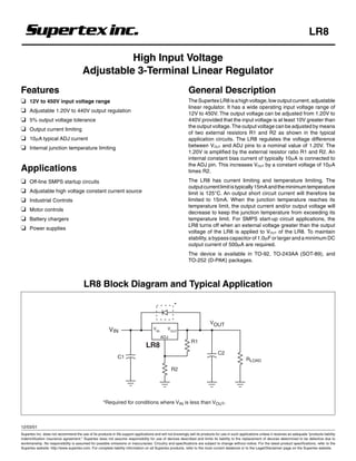
  • 1. LR8 LR8 High Input Voltage Adjustable 3-Terminal Linear Regulator Features General Description ❏ 12V to 450V input voltage range The Supertex LR8 is a high voltage, low output current, adjustable linear regulator. It has a wide operating input voltage range of ❏ Adjustable 1.20V to 440V output regulation 12V to 450V. The output voltage can be adjusted from 1.20V to ❏ 5% output voltage tolerance 440V provided that the input voltage is at least 10V greater than the output voltage. The output voltage can be adjusted by means ❏ Output current limiting of two external resistors R1 and R2 as shown in the typical ❏ 10µA typical ADJ current application circuits. The LR8 regulates the voltage difference ❏ Internal junction temperature limiting between VOUT and ADJ pins to a nominal value of 1.20V. The 1.20V is amplified by the external resistor ratio R1 and R2. An internal constant bias current of typically 10µA is connected to the ADJ pin. This increases VOUT by a constant voltage of 10µA Applications times R2. ❏ Off-line SMPS startup circuits The LR8 has current limiting and temperature limiting. The output current limit is typically 15mA and the minimum temperature ❏ Adjustable high voltage constant current source limit is 125°C. An output short circuit current will therefore be ❏ Industrial Controls limited to 15mA. When the junction temperature reaches its temperature limit, the output current and/or output voltage will ❏ Motor controls decrease to keep the junction temperature from exceeding its ❏ Battery chargers temperature limit. For SMPS start-up circuit applications, the LR8 turns off when an external voltage greater than the output ❏ Power supplies voltage of the LR8 is applied to VOUT of the LR8. To maintain stability, a bypass capacitor of 1.0µF or larger and a minimum DC output current of 500µA are required. The device is available in TO-92, TO-243AA (SOT-89), and TO-252 (D-PAK) packages. LR8 Block Diagram and Typical Application * VOUT VIN VIN VOUT ADJ R1 LR8 C2 C1 RLOAD R2 *Required for conditions where VIN is less than VOUT. 12/03/01 Supertex Inc. does not recommend the use of its products in life support applications and will not knowingly sell its products for use in such applications unless it receives an adequate "products liability indemnification insurance agreement." Supertex does not assume responsibility for use of devices described and limits its liability to the replacement of devices determined to be defective due to workmanship. No responsibility is assumed for possible omissions or inaccuracies. Circuitry and specifications are subject to change without notice. For the latest product specifications, refer to the Supertex website: http://www.supertex.com. For complete liability information on all Supertex products, refer to the most current databook or to the Legal/Disclaimer page on the Supertex website. 1
  • 2. LR8 Ordering Information Package Options Product marking for TO-243AA: TO-92 TO-243AA* TO-252 LR8❋ LR8N3 LR8N8 LR8K4 where ❋ = 2-week alpha date code * Same as SOT-89. Product supplied on 2000 piece carrier tape reels. Absolute Maximum Ratings Pin Configurations VIN Input Voltage -0.5V to +480V* 2 (TAB) Output Voltage Range -0.5V to +470V TAB 1 2 Operating Ambient Temperature Range -40°C to +85°C 3 1 3 Operating Junction Temperature Range -40°C to +125°C TO-243AA (SOT-89) 123 TO-252 Storage Temperature Range -65°C to +150°C TO-92 (D-PAK) *Voltages referenced to ADJ. VIN VOUT ADJ TO-92 1 2 3 TO-243AA 1 2, TAB 3 TO-252 1 2 (TAB) 3 Electrical Characteristics Test conditions unless otherwise specified: -40°C < TA < 85°C. Symbol Parameter Min Typ Max Units Test Conditions VIN - VOUT Input to Output Voltage Difference 12 450 V VOUT Overall Output Voltage Regulation 1.14 1.20 1.26 V 12V<VIN<400V, R1=2.4KΩ, R2=0 VOUT Overall Output Voltage Regulation 375 400 425 V R1=2.4KΩ, R2=782KΩ ∆VOUT Line Regulation 0.003 0.01 %/V 15V<VIN<400V, VOUT=5V, IOUT=0.5mA ∆VOUT Load Regulation 1.4 3.0 % VIN=15V, VOUT=5V, 0.5mA<IOUT<10mA ∆VOUT Temperature Regulation -1 +1 % VIN=15V, VOUT=5V, IOUT=10mA, -40°C<TA<85°C IOUT Output Current Limit 10 20 mA TJ < 85°C, VIN - VOUT = 10V IOUT Output Current Limit 0.5 mA TJ > 125°C, VIN - VOUT = 450V IOUT Minimum Output Current 0.3 0.5 mA Includes R1 and load current IADJ Adjust Output Current 5 10 15 µA C2 Minimum Output Load Capacitance 1 µF DVOUT/DVIN Ripple Rejection Ratio 50 60 dB 120Hz, VOUT = 5V TLIMIT Junction Temperature Limit 125 °C 2
  • 3. LR8 Thermal Characteristics Package Power Dissipation θJC θJA @ TA=25°C °C/W °C/W TO-92 0.74W 125 170 TO-243AA 1.6W 15 78† TO-252 2.5W 6.25 50† † Mounted on FR4 board, 25mm x 25mm x 1.57mm. Significant PD increase possible on ceramic substrate. Functional Block Diagram VIN Pass LR8 VOUT Element Overtemp & Overcurrent 1.2V 10µA ADJ 3
  • 4. LR8 Typical Application Circuits * VOUT=5.0V VIN=15V to 450V V V IN OUT ADJ LR8 R1 6.04KΩ ±1% C2 C1 1.0µF RLOAD ≤16.5KΩ R2 18.2KΩ ±1% VOUT = 1.20V 1+ R2 + IADJ R2 R1 Figure 1: High Input Voltage, 5.0V Output Linear Regulator * Required for conditions where VIN is less than VOUT. VIN=15V to 450V + VAuxiliary Vout1 LR8 - V IN VOUT + ADJ Vout2 Vcc - FB PWM IC Figure 2: SMPS Start-Up Circuit 1µF 1.20V LR8 IOUT = R + VIN VOUT ADJ R VIN = 15V to 450V Load - Figure 3: High Voltage Adjustable Constant Current Source 4
  • 5. LR8 Typical Performance Curves Temperature Variation 1.30 1.25 VIN VOUT=1.2V LR8 VOUT (V) 1.20 ADJ 1.15 12V 2.4KΩ 1.0µF 1.10 1.05 1.00 -50 -25 0 25 50 75 100 125 T(junction) (°C) Adjustment Current 12 11 VIN VOUT=1.2V IADJ (µA) 10 LR8 VIN = 400V 12V, ADJ 9 VIN = 12V 200V, 2.4KΩ 1.0µF 400V I 8 ADJ VIN = 200V 7 6 -50 -25 0 25 50 75 100 125 T(junction) (°C) Load Regulation 5.2 V V =5.0V IOUT IN OUT LR8 5.1 VOUT (V) ADJ 6.04KΩ ±1% 1.0µF 5.0 25V RLOAD 18.2KΩ ±1% 4.9 4.8 0 2 4 6 8 10 IOUT (mA) 5
  • 6. LR8 Typical Performance Curves VOUT vs. VIN 6 VIN VOUT=5.0V 5 LR8 4 VOUT (V) ADJ 6.04KΩ ±1% 0V to 50V 1.0µF 1KΩ 3 18.2KΩ ±1% 2 1 0 0 10 20 30 40 50 VIN (V) Ripple Rejection -65 Ripple Rejection Ratio (dB) VIN VOUT =5.0V IOUT -64 LR8 ADJ 6.04KΩ -63 20VP-P ±1% @ 60Hz 1.0µF RLOAD -62 65V 18.2KΩ ±1% -61 -60 0 2 4 6 8 10 IOUT (mA) 6
  • 7. LR8 Typical Performance Curves Load Transient Response VIN VOUT=5.0V LR8 Closed SW ADJ 6.04KΩ SW Open ±1% 25V 1.0µF 10KΩ 18.2KΩ 523 Ω Vout ±1% Load Transient Response Line Transient Response 400V 400V VIN VOUT VIN LR8 0V ADJ 6.04KΩ Vin ±1% 1.0µF 10KΩ 5.0V 18.2KΩ 0V ±1% Vout 0V Line Transient Response 400V 400V Vin Vin 0V 0V 5.0V 5.0V Vout Vout 0V 0V Line Power Up Transient Line Power Down Transient 12/03/01rev.2 1235 Bordeaux Drive, Sunnyvale, CA 94089 TEL: (408) 744-0100 • FAX: (408) 222-4895 ©2001 Supertex Inc. All rights reserved. Unauthorized use or reproduction prohibited. 7 www.supertex.com
  • 8. LR8 LR8 Application Note AN-H40 High Voltage Linear Regulators and Constant Current Sources Using LR8 by Scott Lynch, Senior Applications Engineer Introduction Operation The LR8 is a high voltage 3-terminal adjustable linear regulator. Except for it’s higher voltage rating, the LR8 operates like any Intended for operation directly off rectified AC mains, the LR8 other 3-terminal adjustable linear regulator. operates at input voltages up to 450 volts, making it compatible A simple resistive divider sets the output voltage while a capacitor with line voltages up to 240 VAC. It’s output voltage adjustability at the output improves transient response and ensures regulator assures that it can be used in most any application. The LR8 is stability. When applicable, an input capacitor is required to ideally suited for low power off-line DC power supplies and provide energy storage for rectified AC. SMPS start-up circuits. Keeping in mind that the LR8 requires at least a 10V difference Available in a leaded TO-92 package and a surface mount between input and output for proper operation, the minimum SOT-89 and D-PAK package, it is ideal for applications where value for CIN is: space is at a premium. Relevant specifications are shown in the table below. t CIN > I LOAD VIN ( pk ) − VOUT − 10V LR8 Specifications where ILOAD = Load current Input Voltage Range (VOUT +10V) to 450V t = Time between peaks of input Output Voltage Range 1.2V to (VIN - 10V) waveform VIN(pk) = Peak input voltage Output Voltage Accuracy ±5% VOUT = Output voltage Power Dissipation TO-92: 0.74W TO-243AA (SOT-89): 1.6W TO-252 (D-PAK): 2.5W Note that the LR8 requires a minimum of 0.5mA load current for proper operation. The current through the resistive divider may Output Current 0.5 to 10mA be included as part of the minimum load. Load Regulation 3% Line Regulation 0.01%/V Supply Rejection 60dB typ @120Hz LR8 Block Diagram and Typical Application Needed for protection should V OUT exceed V IN  R  VOUT = 1.2 v1 + 2  + 10µA • R2  R1  VIN Pass LR8 VOUT Supply Element Load R1 Overtemp & Overcurrent 1.2V 10µA ADJ CIN COUT ≥ 1µF R2 8
  • 9. LR8 Constant Current Operation The LR8 may be configured to provide a constant current output. The current is independent of both supply voltage and load impedance. Constant current operation finds application in driving LEDs and trickle-charging NiCad batteries, as shown below. The trickle charger is for applications that require battery backup (i.e. no cycling), such as emergency lights. Constant Current LED Driver NiCad Battery Trickle Charger R R LR8 LR8 15V to 15V 450V to 450V Start-up Circuit The schematic below depicts a simplified off-line switching power supply using the LR8 for start-up. When VBOOT rises above the LR8’s output voltage, the LR8 goes into standby mode, consuming very little current. All current is then supplied from the bootstrap circuit rather than from the high voltage source, increasing overall efficiency. The output voltage of the LR8 should be set high enough above the minimum operating voltage of the PWM controller, yet low enough to ensure the bootstrap circuit takes over after start-up. With 240VAC input, instantaneous power dissipation can reach 3.4W (340VDC * 10mA). This level exceeds the LR8’s rating, but exists for only as long as it takes for the supply to bootstrap. Thermal mass will prevent die temperature from rising quickly. If boot time is short, die temperatures will not reach the overtemperature protection trip point. It is advisable to mount the LR8 on 2 oz. copper with an area of at least 2.5 square centimeters. Startup Current for Off-line Switching Power Supply bootstrap winding VBOOT D1 VIN VOUT PWM LR8 Controller AC R1 Mains CIN COUT R2 9
  • 10. LR8 Comparison with Discrete Startup Implementations The LR8 provides several advantages when compared with discretely implemented start-up circuits. Zener Implementation Transistor Implementation LR8 Implementation VIN VOUT VIN VOUT VIN LR8 VOUT Disadvantages • Continues to draw current from high voltage source after supply has bootstrapped, resulting in inefficiencies Advantages • Bias must be set for minimum input voltage, resulting in • LR8 goes into standby mode after supply has high current drain at high input voltages bootstrapped, drawing no current from high voltage • Poor regulation input • No current limit • Good regulation • No overtemperature protection • Built-in current limiting • In the Zener implementation, requires large power resistor • Overtemperature protection and Zener Exceeding LR8’s Current Limit for Startup Applications The LR8 has a built-in current limit of 10mA minimum. If the current drawn by the PWM controller exceeds this limit, the LR8 may still be used. To do this, the LR8’s output capacitor supplies a portion of the current until the power supply can bootstrap itself and the LR8 is no longer needed. The following figure graphically illustrates how this is accomplished. Most PWM controllers have an undervoltage lockout (UVL) circuit or programmable start/stop voltages. When the voltage supplied to the PWM controller reaches the turn-on threshold, the controller begins operating and consuming current. If current exceeds the current limit for the LR8, the voltage at VOUT begins to decay. With a large enough capacitor, the supply will bootstrap before voltage decays to the turn- off threshold. 1 Input voltage is applied. The LR8 begins operating (in current VIN 1 limiting mode since COUT appears as a short). VOUT begins to rise as COUT charges. The PWM controller draws a small amount of current. VOUT 4 2 The output voltage of the LR8 reaches the PWM controller’s VHYS turn-on threshold. Controller begins operating, drawing current. Bootstrap voltage begins climbing while VOUT decays since current drawn by the controller exceeds the LR8’s current limit. VBOOT tBOOT 2 3 3 Bootstrap voltage reaches the level of the LR8’s output and IPWM takes over. LR8 current drops to zero. 10mA ILR8 4 Power supply reaches steady-state operation. 0mA 10
  • 11. LR8 The minimum capacitance required for given boot-up time is given by the following equation: I PWM − I LIM COUT > t BOOT VHYS where COUT = Capacitor at LR8 output tBOOT = Time required for supply to bootstrap IPWM = Current used by PWM controller ILIM = LR8 current limit (10mA min) VHYS = PWM controller UVL hysteresis Remember that this equation is valid only when PWM current exceeds the LR8’s current limit. 11/30/01rev.1 1235 Bordeaux Drive, Sunnyvale, CA 94089 TEL: (408) 744-0100 • FAX: (408) 222-4895 11 www.supertex.com