
Recomendados
Más contenido relacionado
La actualidad más candente
La actualidad más candente (20)
Similar a Video DIsplay Technologies
Similar a Video DIsplay Technologies (20)
Más de Varunjeet Singh Rekhi
Último
Último (20)
Video DIsplay Technologies
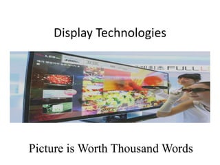
- 1. Display Technologies Picture is Worth Thousand Words
- 2. Contents • Liquid Crystal Display • Organic Light Emitting Diodes • Digital Light Processing • Plasma Display Panels • Field Emission Display • Electronic Ink Displays • Cathode Ray Tube
- 4. Liquid Crystal Display • Liquid crystals can be classified into three different groups, nematic, smectic, an cholestric depending on the level of order in their molecular structure. • Liquid crystals in the nematic group are most commonly used in LCD production. • In the nematic phase, liquid crystal molecules are oriented on average along a particular direction. By applying an electric or magnetic field, the orientation of the molecules can be manipulated in a predictable manner.
- 5. Liquid Crystal Cell • The ability to control how their molecules are naturally arranged is needed. • In their natural state, liquid crystal molecules are loosely ordered with their long axes parallel. • To change this arrangement they are placed onto a finely grooved surface. • When they come into contact with a finely grooved surface also called the alignment layer, the molecules line up parallel along the grooves.
- 6. •Light sent through the twisted liquid crystal structure curls following the molecular arrangement. By changing the orientation of the liquid crystals, light propagating through also changes to follow.
- 7. Conductive electrodes are used to apply voltage to the liquid crystal cell. When a voltage is applied the molecules straighten out aligning parallel to the applied electric field; this also allows propagating light to pass directly through.
- 8. Polarizing Lenses • Polarizer are materials that contain the electric and magnetic fields of a light wave to one plane; all components not within the plane are filtered out. • Set parallel to one another polarizing filters will allow light to pass in only one plane. • When the filters are set in opposite directions or perpendicular to one another, light passes through the first filter but is blocked by the second one.
- 9. Operation of a Simple Liquid Crystal Display • The individual components (glass casing, liquid crystal cell, alignment layer, conductive electrodes, and polarizer) are combined. • Light entering the display is guided by the orientation of the liquid crystal molecules that are twisted by ninety degrees from the top plate to the bottom. • This twist allows incoming light to pass through the second polarizer. When voltage is applied, the liquid crystal molecules straighten out and stop redirecting light.
- 10. • As a result light travels straight through and is filtered out by the second polarizer. • Consequently, no light can pass through, making this region darker compared to the rest of the screen.
- 11. Display Features LCD designs can vary depending on the desired application. • Display format • Resolution • response time • contrast are all features that can vary depending on the desired use.
- 12. Seven –Segment Display • On an LCD information is general displayed in segments or pixels. • Segments are long static regions that can be arranged into different shapes.
- 13. Pixel Grid • Pixels or picture elements are the smallest controllable element on a screen. • A grid of pixels is used to generate various characters; these characters are formed into an array in order to create words and/or sentences.
- 14. • Response time is a measure of how long it takes a pixel to turn from white to black (rise time), and then back again (fall time). • Rise and fall times are controlled by the viscosity of the liquid crystal, the amplitude of the driving voltage, and the thickness of the liquid crystal cell. • For a given liquid crystal compound the cell thickness is usually set, to increase the response time the driving voltage can be increased or the viscosity lowered. • Typical response times for today’s LCD monitors and televisions range from 4ms to 30ms. • Contrast ratio is the difference in brightness between an ‘on’ pixel divided by an ‘off’ pixel.
- 15. Transmission Modes • Three common illumination techniques: • reflective, transmissive, and transflective. • Reflective technology includes a diffuser attached to the lower polarizer; this layer reflects incoming light evenly back through the display. • This type of display relies on ambient light to operate; they will not work in dim lit areas. • Reflective technology is commonly found in calculators and digital wristwatches.
- 16. • Transmissive technologies have backlights attached to the lower polarizer. • Instead of reflecting ambient light, the backlight supplies a light source directly to the display. • Most transmissive displays operate in a negative mode, i.e. that the text will be a light colour and the background a dark colour. • LCDs using transmissive configurations have good picture quality indoors but are barely readable in natural sunlight. • This is due to the intensity of sunlight reflecting from the surface of the LCD which is much stronger than the light coming from the backlight.
- 17. • Transflective devices are a hybrid of the reflective and transmissive schemes. • The construction is similar to transmissive displays except a partially reflective layer is added between the backlight and the liquid crystal. • Since it is a hybrid, transflective screens perform in both indoor and outdoor conditions, but are not as effective as the previous two.
- 18. Liquid Crystal Display Types
- 20. Passive Matrix – a simple grid supplies the charge to a particular pixel on the display. Slow response time and imprecise voltage control. Active Matrix – every pixel has switch and capacitor. A row is switched on, and then a charge is sent down a column. Capacitor holds charge till next cycle. Faster response time, less pixel crosstalk.
- 21. Organic Light Emitting Diodes (OLEDs) • Next trends in display technology is Organic Light Emitting Diodes (OLEDs). • Polymer Light Emitting Diodes (PLEDs) • Small Molecule Light Emitting Diodes (SMOLEDS) and dendrimer technology are all variations of OLEDs. • With all variations being made by electroluminescent substances (substances that emit light when excited by an electric current). • OLED displays are brighter, offer more contrast, consume less power, and offer large viewing angles – all areas where LCDs fall short.
- 22. OLED Working • OLEDs are composed of light-emitting organic material sandwiched between two conducting plates, one of n-type material and one of p- type material. • The molecular structure in n-type material, although electrically neutral, has an extra electron that is relatively free to move around the material. • In p-type material the opposite is true. • The lack of an electron creates a hole that is free to move about. • The creation of the extra electron or the hole comes about because of the mismatch of valence electrons in the molecular structure of the p or n-type material. • Applying a voltage between the two plates causes holes to be injected from the p-type substrate and electrons to be injected from the n-type substrate.
- 23. • When an electron fills in a hole, it drops from a higher energy level to a lower one; consequently, this difference in energy is released as a photon of light (light particle). • The wavelength of the light generated is dependant on the energy gaps of the emitting material. • In order to produce visible light, these energy gaps have to be within 1.5 to 3.5 electron volts (eV). • For example, a photon of 3.1 eV has a wavelength of 400 nm which is visible as a violet light. Therefore, the colors emitted are dependant on the molecular composition of the organic emissive material chosen for the OLED.
- 25. Digital Light Processing (DLP) • DLP technology is a system that uses an optical semiconductor. • This device, known as a Digital Micro mirror Device (DMD chip), is essentially a very precise light switch that can digitally modulate light through the use of 2 million hinge-mounted microscopic mirrors arranged in a rectangular array; each of these micro mirrors are less than 10 microns (approximately one-fifth the width of a human hair). • Combined with a digital video or graphic signal, a light source, and a projection lens, the mirrors of the DMD chip can reflect an all-digital image onto any surface.
- 26. • By mounting these micro mirrors on tiny hinges, they are able to tilt either toward the light source where they are noted as being “on” or away from the light source where they are noted as being “off”. • Depending on the state of these mirrors, a light or a dark pixel is projected onto the screen. • The mirrors are instructed to switch on or off several thousand times per second by a digital signal entering the semiconductor. • A lighter shade of grey is produced when a mirror is switched on more frequently than off; whereby a darker shade of grey is produced when a mirror is switched off more frequently than on. • Using this method, DMD chips can generate up to 1024 shades of grey and consequently produce a highly detailed grey scale image.
- 27. Plasma Display Panels (PDPs) • Plasma displays are noted for their flat screen presentation and large screen sizes. • They are able to generate excellent image quality in large scales, and consequently are the leading display technology when it comes to HDTV
- 29. • Plasma screens are composed of millions of cells sandwiched between two panels of glass. • Placed between the glass plates extending across the entire screen, are long electrodes known as address electrodes and display electrodes which form a grid. • The address electrodes are printed onto the rear glass plate. • The transparent display electrodes, insulated by a dielectric material and covered by a protective magnesium oxide layer, are located above the cells along the front glass plate. • The electrodes intersecting a specific cell are charged in order to excite a xenon and neon gas mixture contained within each cell.
- 30. • When the gas mixture is excited creating a plasma, it releases ultraviolet light which then excites the phosphor electrons located on the sides of the cells. When those electrons revert back to their original lower energy state, visible light is emitted. • Each PDP pixel is composed of three cells containing red, green, and blue phosphors respectively. • Activating these color combinations at varying intensities, by the amount of current generated, results in the color generation as seen on the display.
- 31. Field Emission Displays (FED’s) • The foundation is, extraction of electrons from a material using the “tunnelling” effect. • Tunnelling describes the phenomenon of electrons being able to behave likes waves as well as like particles. • Within a conductor, free electrons are generally mobile within a certain degree. • Potential energy barrier prevents these electrons from simply escaping the bounds of conductors. • Electrons must have enough energy to surpass this potential energy barrier. • With the tunnelling, if a high electric field is applied outside the conductor, the strength of the potential energy barrier will reduce, and will get to the point where an electron wave can extend itself across the barrier.
- 32. • The emitted current, or moving electrons, depends on the electric field strength, the emitting surface, and the work function. • In order for field emission to function, the electric field has to be extremely high: up to 3 x 10⁷ V/cm. • This value is achieved by the fact that field amplification increases with a decreasing curvature radius indicating that the pointier the object, the more charge it will have at its tip, and hence the larger the electric field. • As a result, if such a material can be found, a moderate voltage will cause the tunnelling effect, and hence allow electrons to escape into free space without the heating of the cathode like the traditional Cathode Ray Tube (CRT) technology.