The document summarizes the tunnel diode (Esaki diode), a heavily doped p-n junction diode that exhibits negative resistance. It was introduced in 1958 and shows quantum tunneling effects even at low voltages due to its extremely narrow depletion width of around 100 angstroms. The tunnel diode has an I-V characteristic curve with a peak current and valley current, producing a negative resistance region that can be modeled with an equivalent circuit of a junction capacitance in parallel with a negative resistance.
1. TUNNEL DIODE (Esaki Diode)
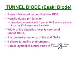
• It was introduced by Leo Esaki in 1958.
• Heavily-doped p-n junction
– Impurity concentration is 1 part in 10^3 as compared to
1 part in 10^8 in p-n junction diode
• Width of the depletion layer is very small
(about 100 A).
• It is generally made up of Ge and GaAs.
• It shows tunneling phenomenon.
• Circuit symbol of tunnel diode is :
EV
2. WHAT IS TUNNELING
• Classically, carrier must have energy at least
equal to potential-barrier height to cross the
junction .
• But according to Quantum mechanics there is
finite probability that it can penetrate through the
barrier for a thin width.
• This phenomenon is
called tunneling and
hence the Esaki Diode
is know as
Tunnel Diode.
3. - Ve Resistance Region
Vf
Vp
Ip
Vv
Forward Voltage
Reverse
voltage
Iv
Reverse
Current
Forward
Current
Ip:- Peak Current
Iv :- Valley Current
Vp:- Peak Voltage
Vv:- Valley Voltage
Vf:- Peak Forward
Voltage
CHARACTERISTIC OF TUNNEL DIODE
4. ENERGY BAND DIAGRAM
Energy-band diagram of pn junction in thermal equilibrium in which both the n
and p region are degenerately doped.
5. -Zero current on the I-V diagram;
-All energy states are filled below EF on both sides of the junction;
AT ZERO BIAS
Simplified energy-band diagram and I-V characteristics of the tunnel diode at zero bias.
6. -Electrons in the conduction band of the n region are directly opposite to
the empty states in the valence band of the p region.
-So a finite probability that some electrons tunnel directly into the empty
states resulting in forward-bias tunneling current.
AT SMALL FORWARD VOLTAGE
Simplified energy-band diagram and I-V characteristics of the tunnel diode at a slight forward bias.
7. -The maximum number of electrons in the n region are opposite to the
maximum number of empty states in the p region.
- Hence tunneling current is maximum.
AT MAXIMUM TUNNELING CURENT
Simplified energy-band diagraam and I-V characteristics of the tunnel diode at a forward bias
producing maximum tunneling current.
8. -The forward-bias voltage increases so the number of electrons on the n side,
directly opposite empty states on the p side decreases.
- Hence the tunneling current decreases.
AT DECREASING CURRENT REGION
Simplified energy-band diagram and I-V characteristics of the tunnel diode at a higher forward
bias producing less tunneling current.
9. -No electrons on the n side are directly opposite to the empty
states on the p side.
- The tunneling current is zero.
-The normal ideal diffusion current exists in the device.
AT HIGHER FORWARD VOLTAGE
Simplified energy-band diagram and I-V characteristics of the tunnel diode at a forward bias
for which the diffusion current dominates.
10. - Electrons in the valence band on the p side are directly opposite to
empty states in the conduction band on the n side.
-Electrons tunnel directly from the p region into the n region.
- The reverse-bias current increases monotonically and rapidly with
reverse-bias voltage.
AT REVERSE BIAS VOLTAGE
11. Cj -R
rs
Ls
TUNNEL DIODE EQUIVALENT CIRCUIT
•This is the equivalent
circuit of tunnel diode
when biased in negative
resistance region.
•At higher frequencies the
series R and L can be
ignored.
•Hence equivalent circuit can be reduced to parallel
combination of junction capacitance and negative
resistance.