
Recomendados
Más contenido relacionado
La actualidad más candente
La actualidad más candente (20)
Similar a Fpga lecture
Similar a Fpga lecture (20)
Último
Último (20)
Fpga lecture
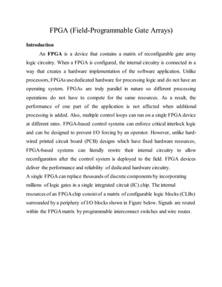
- 1. FPGA (Field-Programmable Gate Arrays) Introduction An FPGA is a device that contains a matrix of reconfigurable gate array logic circuitry. When a FPGA is configured, the internal circuitry is connected in a way that creates a hardware implementation of the software application. Unlike processors, FPGAs usededicated hardware for processing logic and do not have an operating system. FPGAs are truly parallel in nature so different processing operations do not have to compete for the same resources. As a result, the performance of one part of the application is not affected when additional processing is added. Also, multiple control loops can run on a single FPGA device at different rates. FPGA-based control systems can enforce critical interlock logic and can be designed to prevent I/O forcing by an operator. However, unlike hard- wired printed circuit board (PCB) designs which have fixed hardware resources, FPGA-based systems can literally rewire their internal circuitry to allow reconfiguration after the control system is deployed to the field. FPGA devices deliver the performance and reliability of dedicated hardware circuitry. A single FPGA can replace thousands of discrete components by incorporating millions of logic gates in a single integrated circuit (IC) chip. The internal resources of an FPGAchip consistof a matrix of configurable logic blocks (CLBs) surrounded by a periphery of I/O blocks shown in Figure below. Signals are routed within the FPGAmatrix by programmable interconnect switches and wire routes.
- 2. Figure 1: Internal structure of FPGA In an FPGA logic blocks are implemented using multiple level low fan-in gates, which gives it a more compact design compared to an implementation with two- level AND-OR logic. FPGA provides its user a way to configure: 1. The intersection between the logic blocks and 2. The function of each logic block. Logic block of an FPGA can be configured in such a way that it can provide functionality as simple as that of transistor or as complex as that of a microprocessor. It can used to implement different combinations of combinational and sequential logic functions. Logic blocks of an FPGA can be implemented by any of the following: 1. Transistor pairs 2. combinational gates like basic NAND gates or XOR gates 3. n-input Lookup tables 4. Multiplexers 5. Wide fan-in And-OR structure.
- 3. Routing in FPGAs consists of wiresegments of varying lengths which can be interconnected via electrically programmableswitches. Density of logic block used in an FPGA depends on length and number of wire segments used for routing. Number of segments used for interconnection typically is a tradeoff between density of logic blocks used and amount of area used up for routing. Simplified version of FPGA internal architecture with routing is shown in Figure 2.. Figure 2: Simplified Internal Structure of FPGA
- 4. FPGA Structural Classification Basic structure of an FPGA includes logic elements, programmable interconnects and memory. Arrangement of these blocks is specific to particular manufacturer. On the basis of internal arrangement of blocks FPGAs can be divided into three classes: Symmetrical arrays This architecture consists of logic elements (called CLBs) arranged in rows and columns of a matrix and interconnect laid out between them shown in Figure.2. This symmetrical matrix is surrounded by I/O blocks which connect it to outside world. Each CLB consists of n-input Lookup table and a pair of programmable flip flops. I/O blocks also control functions such as tri-state control, output transition speed. Interconnects provide routing path. Direct interconnects between adjacent logic elements have smaller delay compared to general purpose interconnect Row based architecture Row based architecture shown in Figure 3.consists of alternating rows of logic modules and programmable interconnect tracks. Input output blocks is located in the periphery of the rows. One row may be connected to adjacent rows via vertical interconnect. Logic modules can be implemented in various combinations. Combinatorial modules contain only combinational elements which Sequential modules contain both combinational elements along with flip flops. This sequential module can implement complex combinatorial-sequential functions. Routing tracks are divided into smaller segments connected by anti-fuse elements between them. Hierarchical PLDs This architecture is designed in hierarchical manner with top level containing only logic blocks and interconnects. Each logic block contains number of logic modules. And each logic module has combinatorial as well as sequential functional elements. Each of these functional elements is controlled by the programmed memory. Communication between logic blocks is achieved by programmable
- 5. interconnect arrays. Input output blocks surround this scheme of logic blocks and interconnects. This type of architecture is shown in Figure 4. Figure 3: Row based Architecture
- 6. Figure 4: Hierarchical PLDs FPGAClassificationonuser programmable switch technologies FPGAs are based on an array of logic modules and a supply of uncommitted wires to route signals. In gate arrays these wires are connected by a mask design during manufacture. In FPGAs, however, these wires are connected by the user and therefore must use an electronic device to connect them. Three types of devices have been commonly used to do this, pass transistors controlled by an SRAM cell, a flash or EEPROM cell to pass the signal, or a direct connect using antifuses. Each of these interconnect devices have their own advantages and disadvantages. This has a major affect on the design, architecture, and performance of the FPGA. Classification of FPGAs on user programmable switch technology is given in Figure 5. shown below.
- 7. Figure 5: FPGA Classification on user programmable technology Antifuse FPGA Devices are configured by burning a set of fuses. Once the chip is configured, it cannot be altered any more. Hence only one-time programmable. Its logic cells are made up of conventional logic gates. Used for ASIC replacement for small volumes. EEPROM/FlashFPGA The EEPROM/FLASH cell in FPGAs can be used in two ways, as a control device as in an SRAM cell or as a directly programmable switch. Devices may be re-programmed several thousand times and are non-volatile, i.e. keep their configuration after power-off. With only marginal additional effort, the chips may be updated in the field. Re-configuration takes several seconds.
- 8. Static RAM FPGA Currently the dominating technology. Unlimited re-programming. Additional circuitry is required to load the configuration into the FPGA after power on. Re-configuration is very fast, some devices allow even partial re configuration during peration. Allows new approaches & applications like , “Reconfigurable Computing”. FPGA Design Flow One of the most important advantages of FPGA based design is that users can design it using CAD tools provided by design automation companies. Generic design flow of an FPGA includes following steps: System Design At this stage designer has to decide what portion of his functionality has to be implemented on FPGA and how to integrate that functionality with rest of the system. I/O integration with rest of the system Input Output streams of the FPGAare integrated with rest of the Printed Circuit Board, which allows the design of the PCB early in design process. FPGAvendors provide extra automation software solutions for I/O design process. Design Description Designer describes design functionality either by using schematic editors or by using one of the various Hardware Description Languages (HDLs) like Verilog or VHDL. Synthesis Once design has been defined CAD tools are used to implement the design on a given FPGA. Synthesis includes generic optimization, slack optimizations, power optimizations followed by placement and routing. Implementation includes Partition, Place and route. The output of design implementation phase is bit-stream file. Design Verification Bit stream file is fed to a simulator which simulates the design functionality and reports errors in desired behavior of the design. Timing tools are used to determine
- 9. maximum clock frequency of the design. Now the design is loading onto the target FPGAdevice and testing is done in real environment. Hardware design and development The process of creating digital logic is not unlike the embedded software development process. A description of the hardware's structure and behavior is written in a high-level hardware description language (usually VHDL or Verilog) and that code is then compiled and downloaded prior to execution. Of course, schematic capture is also an option for design entry, but it has become less popular as designs have become more complex and the language-based tools have improved. The overall process of hardware development for programmable logic is shown in Figure 6,and described in the paragraphs that follow. Perhaps the most striking difference between hardware and software design is the way a developer must think about the problem. Software developers tend to think sequentially, even when they are developing a multithreaded application. The lines of source codethat they write are always executed in that order, at least within a given thread. If there is an operating system it is used to create the appearance of parallelism, but there is still just one execution engine. During design entry, hardware designers must think-and program-in parallel. All of the input signals are processed in parallel, as they travel through a set of execution engines-each one a series of macrocells and interconnections-toward their destination output signals. Therefore, the statements of a hardware description language create structures, all of which are "executed" at the very same time.
- 10. Figure 6: Programmable logic design process Typically, the design entry step is followed or interspersed with periods of functional simulation. That's where a simulator is used to execute the design and confirm that the correct outputs are produced for a given set of test inputs. Although problems with the size or timing of the hardware may still crop up later, the designer can at least be sure that his logic is functionally correct before going on to the next stage of development. Compilation only begins after a functionally correct representation of the hardware exists. This hardware compilation consists of two distinct steps. First, an intermediate representation of the hardware design is produced. This step is called synthesis and the result is a representation called a netlist. The netlist is device independent, so its contents do not depend on the particulars of the FPGA or CPLD; it is usually stored in a standard format called the Electronic Design Interchange Format (EDIF).
- 11. The second step in the translation process is called place & route. This step involves mapping the logical structures described in the netlist onto actual macrocells, interconnections, and input and output pins. This process is similar to the equivalent step in the development of a printed circuit board, and it may likewise allow for either automatic or manual layout optimizations. The result of the place & route process is a bitstream. This name is used generically, despite the fact that each CPLD or FPGA (or family) has its own, usually proprietary, bitstream format. Suffice it to say that the bitstream is the binary data that must be loaded into the FPGA or CPLD to cause that chip to execute a particular hardware design. Increasingly there are also debuggers available that at least allow for single- stepping the hardware design as it executes in the programmable logic device. But those only complement a simulation environment that is able to use some of the information generated during the place & route step to provide gate-level simulation. Obviously, this type of integration of device-specific information into a generic simulator requires a good working relationship between the chip and simulation toolvendors. Introduction to VHDL The VHSIC Hardware Description Language is an industry standard language used to describe hardware from the abstractto the concrete level. VHDL resulted from work done in the ’70s and early ’80s by the U.S. Department of Defense. Its roots are in the ADA language, as will be seen by the overall structure of VHDL as well as other VHDL statements. VHDL usage has risen rapidly since its inception and is used by literally tens of thousands of engineers around the globe to create sophisticated electronic products. This section will start the process ofeasing the reader into the complexities of VHDL. VHDL is a powerful language with numerous language constructs that are
- 12. capable of describing very complex behavior. Learning all the features of VHDL is not a simple task. Complex features will be introduced in a simple form and then more complex usage will be described. VHDL Terms Before we go any further, let’s define some of the terms that we use throughout the secion. These are the basic VHDL building blocks that are used in almost every description, along with some terms that are redefined in VHDL to mean something different to the average designer. _ Entity. All designs are expressed in terms of entities. An entity is the most basic building block in a design. The uppermost level of the design is the top-level entity. If the design is hierarchical, then the top-level description will have lower- level descriptions contained in it. These lower-level descriptions will be lower- level entities contained in the top-level entity description. _ Architecture. All entities that can be simulated have an architecture description. The architecture describes the behavior of the entity. A single entity can have multiple architectures. One architecture might be behavioral while another might be a structural description of the design. _ Configuration. A configuration statement is used to bind a component instance to an entity-architecture pair. A configuration can be considered like a parts list for a design. It describes which behavior to use for each entity, much like a parts list describes which part to use for each part in the design. _ Package. A package is a collection of commonly used data types and subprograms used in a design. Think of a package as a toolbox that contains tools used to build designs.
- 13. _ Driver. This is a sourceon a signal. If a signal is driven by two sources, then when both sources are active, the signal will have two drivers. _ Bus. The term “bus”usually brings to mind a group of signals or a particular method of communication used in the design of hardware. In VHDL, a bus is a special kind of signal that may have its drivers turned off. _ Attribute. An attribute is data that are attached to VHDL objects or predefined data about VHDL objects. Examples are the current drive capability of a buffer or the maximum operating temperature of the device. _ Generic. A generic is VHDL’s term for a parameter that passes information to an entity. Forinstance, if an entity is a gate level model with a rise and a fall delay, values for the rise and fall delays could be passed into the entity with generics. _ Process. A process is the basic unit of execution in VHDL. All operations that are performed in a simulation of a VHDL description are broken into single or multiple processes. Describing Hardware in VHDL VHDL Descriptions consistof primary design units and secondary design units. The primary design units are the Entity and the Package. The secondary design units are the Architecture and the Package Body. Secondary design units are always related to a primary design unit. Libraries are collections of primary and secondarydesign units. A typical design usually contains one or more libraries of design units. Entity A VHDL entity specifies the name of the entity, the ports of the entity, and entity- related information. All designs are created using one or more entities. Let’s take a look at a simple entity example:
- 14. The keyword ENTITYsignifies that this is the start of an entity statement. In the descriptions shown throughout the book, keywords of thelanguage and types provided with the STANDARD package are shown in ALL CAPITAL letters. For instance, in the preceding example, the keywords are ENTITY, IS, PORT, IN, INOUT, and so on. The standard type provided is BIT. Names of user-created objects suchas mux, in the example above, will be shown in lower case. The name of the entity is mux. The entity has seven ports in the PORT clause. Six ports are of mode IN and one port is of mode OUT. The four data input ports (a, b, c, d) are of type BIT. The two multiplexer select inputs, s0 and s1, are also of type BIT. The output port is of type BIT. The entity describes the interface to the outside world. It specifies the number of ports, the direction of the ports, and the type of the ports. A lot more information can be put into the entity than is shown here, but this gives us a foundation upon which we can build more complex examples. Architectures The entity describes the interface to the VHDL model. The architecture describes the underlying functionality of the entity and contains the statements that model the behavior of the entity. An architecture is always related to an entity and describes the behavior of that entity. An architecture for the counter device described earlier would look like this:
- 15. The keyword ARCHITECTURE signifies that this statement describes an architecture for an entity. The architecture name is dataflow. The entity the architecture is describing is called mux. The reason for the connection between the architecture and the entity is that an entity can have multiple architectures describing the behavior of the entity. Forinstance, one architecture could be a behavioral description, and another could be a structural description. The textual area between the keyword ARCHITECTURE and the keyword BEGIN is where local signals and components are declared for later use. In this example signal select is declared to be a local signal. The statement area of the architecture starts with the keyword BEGIN. All statements between the BEGIN and the END netlist statement are called concurrent statements, because all the statements execute concurrently.
- 16. Concurrent Signal Assignment In a typical programming language such as C or C++, each assignment statement executes one after the other and in a specified order. The order of execution is determined by the order of the statements in the source file. Inside a VHDL architecture, there is no specified ordering of the assignment statements. The order of execution is solely specified by events occurring on signals that the assignment statements are sensitive to. Examine the first assignment statement from architecture behave, as shown here: select<= 0 WHEN s0 = ‘0’ AND s1 = ‘0’ ELSE 1 WHEN s0 = ‘1’ AND s1 = ‘0’ ELSE 2 WHEN s0 = ‘0’ AND s1 = ‘1’ ELSE 3; A signal assignment is identified by the symbol <=. Signal selectwill get a numeric value assigned to it based on the values of s0 and s1. This statement is executed whenever either signal s0 or signal s1 has an event occuron it. An event on a signal is a change in the value of that signal. A signal assignment statement is said to be sensitive to changes on any signals that are to the right of the <= symbol. This signal assignment statement is sensitive to s0 and s1. The other signal assignment statement in architecture dataflow is sensitive to signal select. Let’s take a look at how these statements actually work. Supposethat we have a steady- state condition where both s0 and s1 have a value of 0, and signals a, b, c, and d currently have a value of 0. Signal x will have a 0 value because it is assigned the value of signal a whenever signals s0 and s1 are both 0. Now assume that we cause an event on signal a that changes its value to 1. When this happens, the first signal assignment statement will not execute because this statement is not sensitive to changes to signal a. This happens becausesignal a is not on the right side of the operator. The second signal assignment statement will execute because it is sensitive to events on signal a. When the second signal assignment statement executes the new value of a will be assigned to signal x. Output port x will now change to 1. Let’s now look at the case where signal s0 changes value. Assume that s0 and s1 are both 0, and ports a, b, c, and d have the values 0, 1, 0, and 1, respectively. Now let’s change the value of port s0 from 0 to 1. The first signal assignment statement is sensitive to signal s0 and will therefore execute. When concurrent statements
- 17. execute, the expression value calculation will use the current values for all signals contained in it. When the first statement executes, it computes the new value to be assigned to q from the current value of the signal expression on the right side of the <= symbol. The expression value calculation uses the current values for all signals contained in it. With the value of s0 equal to 1 and s1 equal to 0, signal selectwill receive a new value of 1. This new value of signal selectwill cause an event to occuron signal select, causing the second signal assignment statement to execute. This statement will use the new value of signal select to assign the value of port b to port x. The new assignment will cause port x to change from a 0 to a 1. For the example below, we will be creating a VHDL file that describes an And Gate. As a refresher, a simple And Gate has two inputs and one output. The output is equal to 1 only when both of the inputs are equal to 1. Below is a picture of the And Gate that we will be describing with VHDL. An And Gate Let's get to it! The fundamental unit of VHDL is called a signal. Fornow let’s assume that a signal can be either a 0 or a 1 (there are actually other possibilities, but we will get to that). Here is some basic VHDL logic: 1 2 signal and_gate : std_logic; and_gate <= input_1 and input_2; The first line of codedefines a signal of type std_logic and it is called and_gate. Std_logic is the type that is most commonly used to define signals, but there are others that you will learn about. This codewill generate an AND gate with a single output (and_gate) and 2 inputs (input_1 and input_2). The keyword “and” is reserved in VHDL. The <= operator is known as the assignment operator. When
- 18. you verbally parse the codeabove, you can say out loud, “The signal and_gate GETS input_1 and-ed with input_2.” Now you may be asking yourself where input_1 and input_2 come from. Well as their name implies they are inputs to this file, so you need to tell the tools about them. Inputs and outputs to a file are defined in an entity. An entity contains a port that defines all inputs and outputs to a file. Let’s create a simple entity: 1 2 3 4 5 6 7 entity example_and is port ( input_1 : in std_logic; input_2 : in std_logic; and_result : out std_logic ); end example_and; This is your basic entity. It defines an entity called example_and and 3 signals, 2 inputs and 1 output, all of which are of type std_logic. One other VHDL keyword is needed to make this complete and that is architecture. An architecture is used to describe the functionality of a particular entity. Think of it a thesis paper: the entity is the table of contents and the architecture is the content. Let’s create an architecture for this entity: 1 2 3 4 5 6 architecture rtl of example_and is signal and_gate : std_logic; begin and_gate <= input_1 and input_2; and_result <= and_gate; end rtl; The above codedefines an architecture called rtl of entity example_and. All signals that are used by the architecture must be defined between the “is” and the “begin” keywords. The actual architecture logic comes between the “begin” and the “end” keywords. You’re almost done with this file. One last thing you need to tell the tools is which library to use. A library defines how certain keywords behave in your file. For now, just take it for granted that you need to have these 2 lines at the top of your file: 1 2 library ieee; use ieee.std_logic_1164.all;
- 19. You have created your first VHDL file. You can see the completed file here: 1 2 3 4 5 6 7 8 9 10 11 12 13 14 15 16 17 library ieee; use ieee.std_logic_1164.all; entity example_and is port ( input_1 : in std_logic; input_2 : in std_logic; and_result : out std_logic ); end example_and; architecture rtl of example_and is signal and_gate : std_logic; begin and_gate <= input_1 and input_2; and_result <= and_gate; end rtl; Convert MATLAB code intoVHDL code: Introduction MATLAB means matrix laboratory. It is a powerful tooluse to design any mathematical model very easily and check there result. MATLAB has several specifications but by using MATLAB the analysis of hardware design is not possible it gives the software analysis and results using its calculation in matrix form. To analyze hardware, VHDL codes and VERILOG codes are used by which implementation of that codecan be made possible on target device. Now a major question rises is MATLAB codeable to convert its software design in any hardware descriptive language and the answer comes itself by using HDL coder in MATLAB. HDL coderis work as a bridge which connects two different software MATLAB and HDL software. HDL coderone can convert .m codeto .VHD code or it can change the MATLAB codeto VHDL codeso that it can implement on FPGAkit. Main advantage of HDL coderis that it gives the elapsed time to execute the program. To convert code, initially it is compulsory to convert floating
- 20. point design (MATLAB code)to fixed point design in which every variable length is fixed to a particular no of bits for MATLAB® Version 7.3 (R2006b) added supportfor 64-bit indexing. With 64-bit indexing, we can create variables with up to (2^48) - 1 elements on 64-bit platforms [1]. Floating and Fixed Point Variables Digital signal processingcan be divided into two categories fixed and floating points. This refers to format used to store and manipulate no. within devices. Fixed point DSPs are usually representing no. in bit form of different length (16 bit or more) [2]. Floating point DSP refers to the values where variable size is not fixed. MATLAB codeis a floating point design and HDL codeis a fixed point design. HDL Coder HDL coderis a coderin MATLAB which is used to covert .m codeinto .VHD codeso that the codecan run for FPGAand ASIC design. It is target independent for Xilinx and Altera FPGA’s. This codersupports only MATLAB functions it provides an advisor which can generate VHDL codes. HDL coderis open using codercommand. Thosecommands ask to open earlier project or to create new project. “Figure 1: Project creation for code conversion”
- 21. After opening earlier project or creating new project that HDL coderit is required to create MATLAB test bench and MATLAB function. After creating MATLAB function and test bench the compilation of the codeis required that is completed by MEX compiler. MEX COMPILER - A MEX compiler is a compiler which create a binary mex file of the source code.MEX-files generated using Microsoft Windows. Software Development Kit (SDK) require that Microsoft Visual Studio 2010 run-time libraries be available on the computer they are run on[1]. Before the conversion of the codeto VHDL initially a compilation has to take place on system by a command – Mex –setup The workflow of the command Mex-setup is shown in the dialog box below: >> mex –setup Welcome to mex -setup. This utility will help you set up a default compiler. Fora list of supported compilers, see http://www.mathworks.com/support/compilers/R2012a/win32.html Please chooseyour compiler for building MEX-files: Would you like mex to locate installed compilers [y]/n? y Selecta compiler: [1] Lcc-win32 C 2.4.1 in D:matlabsyslcc [0] None Compiler: 1 Please verify your choices: Compiler: Lcc-win32 C 2.4.1 Location:D:matlabsyslcc Are these correct[y]/n? y Trying to update options file: C:UsersabcAppDataRoamingMathWorksMATLABR2012amexopts.bat From template: D:matlabbinwin32mexoptslccopts.bat Done . . . After completion of mex compilation HDL coderasks to add MATLAB function and test bench.
- 22. “Figure 2: Entry points of HDL coder” After adding function and test bench a advisor is available in the HDL coderwhich is used to run MATLAB codeand generate VHDL code. If advisor does not run successfully then error has to be removed from the .m code. And if it runs successfully then 3 files are generated: 1. pkg.vhd (package file of VHDL code.) 2. cod.vhd (VHDL code.) 3. tb.vhd (test bench of code.) The advisor in HDL coderis shown below.
- 23. “Figure 3: Advisor” After these steps HDL codeconversion of MATLAB code successfully take place. After that completion one more report is generated which is an .html file. That file shows the resource utilization of generated VHDL codeor it told how many adders, subtractors, multipliers, and multiplexers are required to implement that design in hardware [3]. The generated codeis now synthesized in the software of front end designing i.e. XILINX. After all these models a synthesize report [4] is generated which tells summary of the whole design. The major reports generated in synthesizing are: 1: Synthesis Options Summary 2: HDL Parsing 3: HDL Elaboration 4: HDL Synthesis 4.1: HDL Synthesis Report 5: Advanced HDL Synthesis 5.1: Advanced HDL Synthesis Report 6: Low Level Synthesis 7: Partition Report 8: Design Summary 8.1: Primitive and Black Box Usage
- 24. 8.2: Device utilization summary 8.3: Partition ResourceSummary 8.4: Timing Report 8.4.1: Clock Information 8.4.2: Asynchronous Control Signals Information 8.4.3: Timing Summary 8.4.4: Timing Details After all the above report finally converted codesuccessfully runs in XILINX [5]. For the better understanding of hardware we can check different model of our converted code. Major models which are used to check the hardware are: 1: RTL model. 2: Technology schematic model. Above model finally gives us the hardware look of the converted MATLAB code and our problem of defining hardware from MATLAB codegot resolved. The code conversioncanbe shownin a flow graph: “Figure 4: Flow Chart of HDL Coder Workflow”