Chapter 6b
•Descargar como PPTX, PDF•
2 recomendaciones•1,719 vistas

Optoelectronics Lecture notes

Recomendados
Más contenido relacionado
La actualidad más candente
La actualidad más candente (20)
Destacado
Destacado (20)
Similar a Chapter 6b
Similar a Chapter 6b (20)
Más de Gabriel O'Brien
Más de Gabriel O'Brien (20)
Último
Último (20)
Chapter 6b
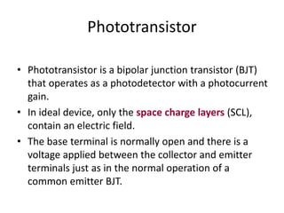
- 1. Phototransistor • Phototransistor is a bipolar junction transistor (BJT) that operates as a photodetector with a photocurrent gain. • In ideal device, only the space charge layers (SCL), contain an electric field. • The base terminal is normally open and there is a voltage applied between the collector and emitter terminals just as in the normal operation of a common emitter BJT.
- 2. n h Base Collector h+ e– Emitter pn+ E e– SCLSCL Iph VBE VBC VCC The principle of operation of the photodiode. SCL is the space charge layer or the depletion region. The primary photocurrent acts as a base current and gives rise to a large photocurrent in the emitter-collector circuit. © 1999 S.O. Kasap,Optoelectronics(Prentice Hall) Fig.6: Phototransistor
- 3. Principle of Phototransistor • An incident photon is absorbed in the SCL between the base and collector to generate an EHP. – The field E in the SCL separates the EHP and drifts them in opposite direction – This is the primary photocurrent and constitutes a base current even the base terminal is open circuit • When the drifting electron reaches the collector, it becomes collected by the battery. • When the hole enters the neutral base region, it can be neutralized by injecting a large number of electrons into the base. – It effectively “forces” a large number of electrons to be injected from the emitter.
- 4. Principle of Phototransistor, cont • Typically, the electron recombination time in the base is very long compared with the time it takes for electrons to diffuse across the base – This means that only a small fraction of electrons injected from the emitter can recombine with holes in the base • Thus, the emitter has to inject a large number of electrons to neutralize this extra hole in the base • These electrons (except one) diffuse across the base and reach the collector and thereby constitute an amplified photocurrent
- 5. Emitter current • Alternatively, the photogeneration of EHPs in the collector SCL decreases the resistance of this region – which decreases the voltage VBC across the base collector junction • Consequently, the base-emitter voltage VBE must increase because of VBE+VBC = VCC • This increase in VBE acts as if it were a forward bias across the base-emitter junction and injects electrons into the base due to the transistor action, – That is the emitter current IE exp (eVBE/kT).
- 6. Current gain • Since the photon generated primary photocurrent Ipho is amplified as if it were a base current (IB), the photocurrent flowing in the external circuit is Iph b Ipho where b is the current gain (or hFE) of the transistor • The phototransistor construction is such that incident radiation is absorbed in the base-collector junction SCL.
- 7. Photoconductive detectors • The photoconductive detectors have the simple structure – Two electrodes are attached to a semiconductor that has the desired absorption coefficient and quantum efficiency over the wavelength of interest. • Incident photons become absorbed in the semiconductor and photogenerate EHPs. – The result is an increase in the conductivity of the semiconductor and hence an increase in the external current which constitutes the photocurrent Iph.
- 8. Photoconductive Gain • The actual response of the detector – depends whether the contacts to the semiconductor are ohmic or blocking (For example Schottky junctions that do not inject carriers) – depends on the nature of carrier recombination kinetics • We will consider a photoconductor with ohmic contacts – The contacts do not limit the current flow • With ohmic contacts, the photoconductor exhibits photoconductive gain – The external photocurrent is due to more than one electron flow per absorbed photon.
- 9. Light w d V Iphoto Asemiconductor slab of length , width w and depth d is illuminated with light of wavelength . n = no + n p = po + p © 1999 S.O. Kasap,Optoelectronics(Prentice Hall) Fig.7: Photoconductive detectors
- 10. Principle of photoconductive detectors • The absorbed photon photogenerates an EHP, which drift in opposite directions. – The electrons drifts much faster than the hole and therefore leaves the sample quickly • The sample must be neutral, which means another electron must enter the sample from the negative electrode – This new electron also drifts across quickly to leave the sample while the hole is still drifting slowly in the sample • Thus another electron must enter the sample to maintain neutrality, and so on, until either the hole reaches the negative electrode or recombines with one of these electrons entering the sample.
- 11. Iph Photoconductor e– h+ Iph Iph Iph Iph A photoconductor with ohmic contacts (contacts not limiting carrier entry) can exhibit gain. As the slow hole drifts through the photoconductors, many fast electrons enter and drift through the photoconductor because, at any instant, the photoconductor must be neutral. Electrons drift faster which means as one leaves, another must enter. (a) (b) (c) (d) (e) © 1999 S.O. Kasap, Optoelectronics(Prentice Hall) Fig.8: Principle of photoconductive detectors
- 12. Gain • The external photocurrent therefore corresponds to the flow of many electrons per absorbed photon, which represents a gain. • The gain depends on the drift time of the carriers and their recombination lifetime
- 13. Noise in Photodetector • The lowest signal that a photodetector can detect is determined by – the extent of random fluctuation in the current through the detector – and the voltage across it as a result of various statistical processes in the device. • When a pn-junction is reverse biased, there is still a dark current Id present – which is mainly due to thermal generation of EHPs in the depletion layer and within diffusion lengths to the depletion layer.
- 14. Dark Current • The dark current exhibits shot noise or fluctuation about Id. • This shot noise is due to the fact that electrical conduction is by discrete charges, – which means that there is a statistical distribution in transit time of the carriers across the photodiode. • Carriers are collected as discrete amounts of charge (e) – that arrive at random times and not continuously.
- 15. Shot noise current: Dark current • The root mean square (rms) value of the fluctuations in the dark current represents the shot noise current: in-dark=[2eId B] ½ (1) where B is the frequency bandwidth of the photodetector. • The photocurrent signal must be greater than this shot noise in the dark current
- 16. Quantum Noise • The photodetection process involves – the interaction of discrete photons with valence electrons. • The discrete nature of photons – means that there is an unavoidable random fluctuation in the rate of arrival of photons • The quantum nature of the photon gives rise to a statistical randomness in the EHP photo-generation process • This type of fluctuation is called quantum noise (photon noise) – It is equivalent to shot noise
- 17. Shot Noise Current: Quantum Noise • The photocurrent will always – exhibit fluctuations about its mean value due to quantum noise. • If Iph is the mean photocurrent, the fluctuations about this mean has an rms value that is called shot noise current due to quantum noise, in-quantum=[2 e Iph B] ½ (2)
- 18. Vout Current Time Id Vr In pn junction and pin devices the main source of noise is shot noise due to the dark current and photocurrent. pn Po Dark IlluminatedId + Iph Id + Iph + in R A © 1999 S.O. Kasap,Optoelectronics(Prentice Hall) Fig.9: Noise in Photodetector
- 19. RMS total shot noise current • Generally, the dark current shot noise and quantum noise are the main sources of noise in pn-junction and pin type photodiodes. • The total shot noise generated by the photodetector is not a simple sum of eqns (1) & (2) because the two processes are due to independent random fluctuations • We need to add the mean squares of the shot noise current i2 n= i2 n-dark + i2 n-quantum i2 n= [2 e (Id + Iph ) B]
- 20. RMS total shot noise current • In Fig.9, the photodetector current, Id flows through a load resistor R – which acts as a sampling resistor for measuring the current. • The voltage across R is amplified • In considering the noise of the receiver, we also include – the thermal noise in the resistor and – noise in the input stage of the amplifier • Thermal noise: random voltage fluctuations across any conductor due to random motions of conduction electrons
- 21. Signal to Noise Ratio • In receiver design, we are often interested in the signal to noise ratio, SNR or S/N, • For the photodetector alone, SNR = I2 ph/ i2 n • For the receiver, SNR must include the noise power generated in the sampling resistor R (thermal noise) and in the input elements of the amplifier. PowerNoise PowerSignal SNR
- 22. Noise Equivalent Power • The noise equivalent power (NEP) is an important property of a photodetector that is frequently quoted. – It is the optical signal power required to generate a photocurrent signal (Iph) that is equal to the total noise current (in) in the photodetector at a given wavelength and within bandwidth of 1 Hz. – It represents the required optical power to achieve a SNR of 1 within a bandwidth of 1Hz • The detectivity, D = 1/NEP
- 23. Quantitative definition of NEP • If R is the responsivity and Po is the monochromatic incident optical power then the generated photocurrent is, Iph = RPo • Suppose Iph = in when Po = P1, Then RP1 = [2 e (Id + Iph ) B] ½ • From this, we find optical power per square root of frequency bandwidth as P1/ B½ = (1/R)[2 e (Id + Iph ) ] ½ • Quantitative definition of NEP = P1/ B½ [W Hz –½] • If we put B = 1 Hz, NEP = P1
- 24. Example: Noise of an ideal photodetector • Consider an ideal photodiode with h =1 (QE=100%) and no dark current Id = 0. Shows that the minimum optical power required for a signal to noise ration (SNR) of 1 is P1 = (2hc/) B Calculate the minimum optical power for an SNR=1 for an ideal photodetector operating at 1300nm with a bandwidth of 1 GHz. What is the corresponding photocurrent?
- 25. Solution B hc P B hc P eB hc Pe I eBII BeIBIIeI iIP ph phd phphdph h h h 2 1,tor,photodetecidealanFor 2 2 ty,responsiviofdefinitiontheFrom 2Thus,0since 22 en,current whnoisethetoequalis(signal)ntphotocurreThe1.SNRthatso ,ntphotocurrethemakesthatpoweropticalincidenttheneedWe 1 1 1 nph1 2 1 2 1
- 26. Solution, 2 .1with/fromcalculatecanweeAlternativ nA0.32orA102.310106.122 is,ntphotocurreingcorrespondThe noise.quantumtodueiscurrentnoiseThe 1,SNRaforsignalminimumtheisThis 0.31nWorW101.3 103.11/1010310626.62/2 GHz,1atandm1.3atoperatingtorphotodetecidealanFor 1 10919 10 1 69834 1 hh h hcPeII eBI P hcBP phph ph