SlideShare una empresa de Scribd logo
1 de 183
Descargar para leer sin conexión
Global Open Source
The GMS Gas Management System designed by Twin Brothers Stanley A Meyer and Stephen Meyer.
Their work was saved preserved re learnt and replicated through 20 + years of discussions on forums.
As far as we know there was no main board made in the original GMS system it was all jumper wires and
looms. Daniel Donatelli designed this “Matrix” main board to make the uptake of the educational work
of relearning, testing and advancing the technologies faster. By achieving this he has removed a lot of
the mystery from the GMS Unit and its operation and card interconnections.
The Design closely follows the original engineering concept to allow easy advancement or swap out of
newer or more advanced board as they are made like SMD or Various versions of safety card or gas feed
back card etc.
By creating this board, we managed to rediscover several of the unknown or unclear areas in the
Original GMS unit that was in the Dune Buggy Stanley A Meyer Built.
The 2020 Remade version and Matrix Main board does not have the Injector cards, exhaust gate EGR
and intake air gate solenoid % cards and distributor cards on the board they were left out intentionally.
This Matric Assembly was designed to allow the modern Drift Race Hot Rod or Engine Tuner to see how
to join or integrate into their ECU/EMS experience and systems.
The Reason is we have more advanced systems now Like Speeduino ECU/EMS or Mega Squirt ECU/Ems
which can be adjusted to handle the job. With a simple TPS linkage to this GMS Matrix card array.
The purpose of this document is to describe what is on the pins of the connectors on the VIC Matrix
card. For some of the cards that plug into VIC Matrix front panel interfaces will also be listed.
Global Open Source
Index (Editing in Process)
• Safety Jump Card Plugs into K1 Page 2
• K2 Connectors on VIC Matrix Card Page 5
• K3 Gated Pulse Frequency Generator Page 8
• K8 Connectors on VIC Matrix Card Page 11
• K11 Connectors on VIC Matrix Card Page 13
• K16 Connectors on VIC Matrix Card Page 16
• KGF1 Gas Feedback Control Page 19
• KA1 - Auto-Start Page 22
• Main Board Matrix Pin out Connectors Page 24
• Main Board Matrix Pin in Connectors Page 26
Here we Show the Basic Concept of how we separated the Gas on demand controls and the ECU /EMS
portion which is now easier with modern Ems ECU systems. This allows a simple linking by the RPS
signal and basic in/out sensor leads.
Global Open Source
The purpose of this document is to describe what is on the pins of the connectors on the VIC Matrix
card. For some of the cards that plug into VIC Matrix front panel interfaces will also be listed.
Note: The numbering on the 37 sub-d in table below start with pin 19 at top of VIC Matrix board
K1 Connectors on VIC Matrix Card
The K1 connectors on the VIC Matrix Card are for the Safety Cards. Card can be either the local
Safety Jump Card or the Operational Safety Card which support other functions and remote
control of the safety function. Pins in use on the 37 pin sub-d connector vary depending on the
card inserted in the connector.
K1 pins in 37 pin sub-d connector listed in table below are directly connected to board
connections points on left of the K1 37 pin connector (see picture below)
VIC Matrix K1 board section
Global Open Source
Pin # K1
Name
Connectors
to Left
Description
19 12V GND Input from 12V Power Regulators
18 5V 5V Input from 5V Power Regulators
17 10V 10V Input from 10V Power Regulators
16 GND 12V Input from Power Regulator GND
15 NC
14 PRESSURE
13 NC
12 TEMP
11 NC
10 RPM
9 NC
8 JAR
7 NC
6 OIL
5 NC
4 12V GND Output on and off board devices
when jumped by Safety Card
3 5V 5V Output on and off board devices
when jumped by Safety Card
2 10V 10V Output on and off board devices
when jumped by Safety Card
1 GND 12V Output on and off board devices
when jumped by Safety Card
20-37 NC
Note: Pins not listed are not connected (NC)
Global Open Source
Ki Safety Control Card Plugs into K1
The Safety Card has switches and sensor triggers which close the power connections on the VIC
MATRIX STANLEY A MEYER backplane card. Such as over speed RPM trigger, over heat oil
trigger, over heat trigger, roll over mercury switch, or a switch that connects to remote grenade
ring pull kill switch. When this card is removed there is no system power to the rest of the
boards plug in the VIC Matrix board. Alternatively can can be replaced with Safety Jump Card.
The board provides jumpers between input and output pins of the 37 pin sub-d connector.
The following pins are in use:
Pin # Board
Name
Description
19 GND Input from Power Regulators
18 5V Input from Power Regulators
17 10V Input from Power Regulators
16 12V Input from Power Regulators
NC
4 GND Output on and off board devices when jumped by
Safety Card
3 5V Output on and off board devices when jumped by
Safety Card
2 10V Output on and off board devices when jumped by
Safety Card
1 12V Output on and off board devices when jumped by
Safety Card
20-37 NC
Note: Pins not listed have no connections (NC)
Global Open Source
Safety Card Sensors and Switch Examples Plugs into Ki Safety Control Card
Safety Jump Card Plugs into K1
The Safety Jump Card closes the power connections on the VIC MATRIX STANLEY A MEYER
backplane card. When this card is removed there is no system power to the rest of the boards
plug in the VIC Matrix board.
In operational use this board can be replace with a board that connects to remote kill switch
The board provides jumpers between input and output pins of the 37 pin sub-d connector.
The following pins are in use:
Pin # Board
Name
Description
19 GND Input from Power Regulators
18 5V Input from Power Regulators
17 10V Input from Power Regulators
16 12V Input from Power Regulators
NC
4 GND Output on and off board devices when jumped by
Safety Card
3 5V Output on and off board devices when jumped by
Safety Card
2 10V Output on and off board devices when jumped by
Safety Card
1 12V Output on and off board devices when jumped by
Safety Card
20-37 NC
Note: Pins not listed have no connections (NC)
Global Open Source
Bare Card Front
Card Back
Finished Card with male pins in connector
Note: Pin type in connector is a builder option though pin on VIC Matrix need to be opposite
sex.
Global Open Source
K2 Connectors on VIC Matrix Card
The K2 connector on the VIC Matrix Card is for the Variable Pulse Frequency Generator Card K2.
On the VIC Matrix Card, the pins on the 37 pin sub-d connector are not labeled, however, the
labels do appear on the K2 card for these pins (show here for reference).
VIC Matrix K2 board section
Pin # K2 Name Connectors
to Left
Description
19 GND GND Input from 12V Power Regulators
18 5V 5V Input from 5V Power Regulators
5 NC NC
4 C to k3 C to k3 Output Frequency generated on K2 card
3 B to K3 B to K3 Output Frequency generated on K2 card
2 Q to K10 Q to K10 Output Frequency generated on K2 card
Also connects to K2 Q to K10 connector on
far right of VIC Matrix Card
1 G to K11 G to K11 Output Frequency generated on K2 card
20-37 NC
Note 1: Pins not listed have no connections (NC)
The is not enough space to left of the K2 37 pin connector to handle all the interface signals
going to the K2 front panel so the follow signals from K2 card go directly to front panel. For
more details see description of K2. This table also provide information on labels for front panel
K2
Name
Description
Aux X Input to switch10x less than 2x
Aux 2X Input to switch 10x less than 3x
Aux 3X Input to switch10x 10x less that 4x
Aux 4X Input to switch10x Highest Freq
Aux COM Output from switch to COM which routes to C
Accel X Input to switch10x less than 2x
Global Open Source
Accel 2X Input to switch 10x less than 3x
Accel 3X Input to switch10x 10x less that 4x
Accel 4X Input to switch10x Highest Freq
Accel COM Output from switch to COM which routes to B
Resonant Run X Input to switch10x less than 2x
Resonant Run 2X Input to switch 10x less than 3x
Resonant Run 3X Input to switch10x 10x less that 4x
Resonant Run 4X Input to switch10x Highest Freq
Resonant Run COM Output from switch to COM which routes to Q
Resonant Dist. X Input to switch10x less than 2x
Resonant Dist. X Input to switch 10x less than 3x
Resonant Dist. X Input to switch10x 10x less that 4x
Resonant Dist. X Input to switch10x Highest Freq
Resonant Dist. COM Output from switch to COM which routes to G
GAS Switch to select Gas setting
WFC Switch to select WFC setting for Freq.
POTB NC
POTA 100k pot Freq Adjustment side1
LED - Negative lead to LED
LED + Positive Lead to LED
POTB 100k pot Freq Adjustment Gas side of switch
POTA 100k pot Freq Adjustment WFC side of switch
GAS Switch position for GAS
WFC Switch Position for WFC
COM Connects GAS or WFC resistor bank to 555 Pin 7
Note 1: Wires on 100K Pot need to connected so frequency is changed in correct direction H-CW
and L-CCW.
Note 2: Need to verify Switch Name Com goes to correct board output name for all 4 switches.
Need to do this so correct switch name is place on switches on front panel for each output.
Note 3: This is case where name are not very helpful in telling you what they do. I expect these
were original functional names and were never updated.
Global Open Source
K2 Variable Pulse Frequency Generator Card
K2 Variable Pulse Frequency Generator Card – Populated without front panel interfaces
Global Open Source
K3 Gated Pulse Frequency Generator
The K3 connector on the VIC Matrix Card is for the Variable Pulse Frequency Generator Card K3.
On the VIC Matrix Card, the pins on the 37 pin sub-d connector are not labeled, however, the
labels do appear on the K3 card for these pins (show here for reference).
VIC Matrix K8 board section
Pin # K3 Name Connectors
to Left
Description
19 - -
18 - -
17 A A Gated pulse out
To K3 A on far right of board
16 - -
15 - -
14 - -
13 10V IN 10V
12 - -
11 - -
10 K To KGT K Left Connector
9
8
7
6
5 B/AUTO B/AUTO K2 Pin 17 (Manual Interface)
4 +5V +5V++++++
3 GND GND
2 M/MANUAL M/MANUAL To M1 Connector to left of KGF1
From M Connector to M1 left of K8
From K11 Pin 19 (Auto Interface)
1 - -
20-37 NC
Note: Connection not shown have No Connection NC
Note: Connections with “-“ are directly connected signal ?
Note: B/Manual and M/Auto labels are switched. Manual signal comes from K3 and Auto
signal from K11. Problem can be fixed by wiring of front panel switch. Wiring on VIC Matrix is
correct.
Global Open Source
K3 Off Board connections to front panel
K3 Name Description
LED Led +
Led -
ACCEL Input M1 from K11
MAN Input Manual in B from K33
SWITCH Selection returned to board
SIGNAL Voltage level into chip to set gate frequency
H/L Center Position of Pot
100K POT VDD into Pot
CELL ON Switch Open (single pole switch)
CELL OFF GND Switch closed
SWITCH NC
TEST Single A put from Gate Generator
GHD
Note: The 100K pot needs to hooked up so CW raises frequency and CCW lowers it
NOTE: There are signals going on the 37 sub-d connector that go chips on the board as they
are not labeled sure what they are.
K3 Gated Pulse – Freq Gen bare board
Global Open Source
K8 Connectors on VIC Matrix Card
The K8 connector on the VIC Matrix Card is for the Analog Voltage Generator Card K8. On the
VIC Matrix Card, the pins on the 37 pin sub-d connector are not labeled, however, the labels do
appear on the K2 card for these pins (show here for reference).
VIC Matrix K8 board section
Pin # K8 Name Connectors
to Left
Description
19 M M Gated Digital Signal in
To test jack on front panel through
Analog/Digital Switch
18 5V 5V
17 50K POT 50K POT Manual Speed Cal - Other side is
GND on front panel
16 12V 12V On left as it goes to one side of 25K
Pot
15 NC
14 RUN ACCE RUN ACCE On leg of switch
13 NC
12 GND GND
11 GND
10 GND
9 NC
8 NC
7 SWITCH SWITCH Manual Speed Cal leg of Switch
6 NC
5 100K POT 100K POT
4 J J Analog signal out in sync with gate
To K8 J on left end of board and
to DB9 pin 3 next to it not labeled
To test jack on front panel through
Analog/Digital Switch
3 NC
2 100K POT 100K POT Gain Limit – Other side is J on front
panel
1 25K POT 25K POT RPM IDLING – Other side is GND on
front panel
Global Open Source
20-37 NC
Note 1: Pins not listed have no connections (NC)
Note 2: Pots on front panel need to be checked so there are wired to have the desired results
increase CW decrease CCW
Note 3: The front panel also has Analog/Digital switch the controls the M and J signals going to
test jack on front panel.
K8 Analog Voltage Generator – bare board
Global Open Source
K11 Connectors on VIC Matrix Card
The K11 connector on the VIC Matrix Card is for the Digital Control Means Card K11. On the VIC
Matrix Card, the pins on the 37 pin sub-d connector are not labeled, however, the labels do
appear on the K11 card for these pins (show here for reference).
VIC Matrix K11 board section
Pin # K11 Name Connectors
to Left
Description
19 M1,M2 M1,M2 Pin 37
18 - -
17 (below M4) To Man/Cal 50K Pot on top of card
16 (below M2)
13 GND Pin 12 & 11 System GND
12 GND Pin 13 & 11 System GND
11 GND Pin 29 System GND
9 J Pin 9 J
37 M1,M2 Pin 19
36 M4 M4
35 M2 M2
34 M3 M3
33 J J
32
31
30 GND To System GND
29
28 5V 5V To System 5V
27 J TPS - TPS Connectors on right in of board
26 J TPS ~ TPS Connectors on right in of board
25 J TPS+ TPS Connectors on right in of board
24 J
23
22 12V 12V To System 12V
21
20 G G Input from G to K9 on Connect to
Left of K2 (Timing signal in from K2)
Global Open Source
+
~
-
Note 1: Pins not listed have no connections (NC)
K11 Off Board connections to front panel
Note: As the output of these show NC it appears these are not being used. These functions all
are on K8 Analog Voltage Generator Card.
K11 Name PIN Description
ACCEL MAX 100K 1 J from P32
2 J from P32
J To Pin 1 A side of A to D Switch
3 Back into board
IDLING 25K POT 1 Pin 7 GND
2 J
3 Pin 14 NC
MAN/RUN SWITCH 1 From Pin 4 NC
To MAN/CAL 50K POT pin 3
2 Pin 10 NC
3 To MAN/CAL 50K POT pin 2
MAN/CAL 50K POT 1 From Pin 4 NC
Pin 3 NC
2 From MAN/RUN SWITCH pin 3
3 From MAN/RUN SWITCH pin 1
To BNC Pin 2 +
DIGL/ANL 1 J from ACELL MAX 100K pin 2
2 BNC pin 1
3 IC1 pin8
BNC 1 - (GND)
From DIGL/ANG switch pin 2
2 + Signal selected by DIGL/ANL switch
From MAN/CAL 50K POT Pin 3
Global Open Source
K11 Digital Control Means - bare board
New Daughter Board Replaces the k7 Laser Accelerator card to allow modern industry standard
TPS sensor input to the GMS and K11 Circuit Assemblies. Designed to be simple use and to allow
industry 3 pin plugs male and female TPS wiring loom plugs and join to the wiring loom
of all cars easily.
Global Open Source
K16 Connectors on VIC Matrix Card
The K16 connector on the VIC Matrix Card is for the Regulated Power Supply K16. On the VIC
Matrix Card, the pins on the 37 pin sub-d connector are not labeled, however, the labels do
appear on the K11 card for these pins (show here for reference).
VIC Matrix K16 board section
Pin # K11
Name
Connectors
to Left
Description
19 - Shunt 1 on board
18 12V 12V
17 10V 10V
16 NC NC
15 5V 5V
14 NC NC
13 GND GND
12 NC
11 - Shunt on board
10 NC
9 12V 12V
8 NC
7 10V 10V
6 NC
5 5V 5V
4 NC
3 GND GND
2 NC
1 NC
20-37 NC
Note: Pins not listed are not connected (NC)
K16 Off Board connections to front panel
K16 Name PIN Description
ROTRAY SWITCH 1 To BNC + test point
Global Open Source
2 Left 10V Blocking Diode
3 Left 5V Blocking Diode
4 Right 10V Blocking Diode
5 Right 5V Blocking Diode
BNC TEST POINT 1 BNC -
2 BBC +
10V LED GREEN 1 - Top half 10V Status light
2 +
ON/OFF SWITCH 1 Normally off – turned on if fuse fails
2
5V LED GREEN 1 - Top half 5V Status light
2 +
10V LED GREEN 1 - Bottom half 10V Status light
2 +
FUSE 1 Fuse for bottom half
2
5V LED GREEN 1 - Bottom half 10V Status light
2 +
Note: If power Regulators are off board then there would be 3 additional connections to each
one.
Global Open Source
K16 Regulated Power Supply Bare Board
Global Open Source
KGF1 Gas Feedback Control
The KGF1 connector on the VIC Matrix Card is for the Gas Feedback Control Card. On the VIC
Matrix Card, the pins on the 37 pin sub-d connector are not labeled, however, the labels do
appear on the Gas Feedback Control card for these pins (show here for reference).
VIC Matrix KGF1 board section
Pin # KGF1 Name Connectors to
Left
Description
19 VEE VEE 10V
18 M1 M1 Input Frequency from K2
17 GND GND System GND
16 10V INPUT 10V INPUT
15 11/12 OUTPUT 11/12 OUTPUT
14 K – GATE
PULSE CARD
K Out to K3 cell on/off control
13 NC
12 12V + 12V + VCC + 12V Input
11 12V - 12V - VCC – 12V Input (GND)
10 VEE VEE 10V
To Trans Signal Input VEE lower right
9 SIGNAL SIGNAL Sensor
To Trans Signal Input Signal lower right
8 GND GND System GND
To Trans Signal Input GND lower right
7 OUT 6 OUT 6 Out to K3 input 6
6 NC
5 NC
4 NC
3 NC
2 NC To J on left side of K8
Global Open Source
1 NC
20-37 NC
Note: Pins not listed are not connected (NC)
KGF1 Off Board connections
This board was designed to support off board connections directly from the board these
connection points are shown here. Most of these points are also in the 37 sub-d connector and
on the connectors to left.
KGF1 Name PIN Description
VEE Cell pressure gage
M1 Cell pressure gage
GND Cell pressure gage
10V INPUT
11/12 OUTPUT
K
Limit Selector 1
2
3
12V + VCC 12V Input
12V- VCC 12V Input
VEE Transducer Signal Input
SIGNAL Transducer Signal Input
GND Transducer Signal Input
6 VIC OUT 6
Note: Limit Selector is the only item that does not have an interface point on VIC Matrix board.
Global Open Source
KGF1 Gas Feedback Control bare board
This is the Original Gas Feed back card from Schematic
KGF2 Gas Feedback Control board was card found in the GMS not completed to db37 yet 90%
done
Global Open Source
GF3 Gas Feedback Control bare board
This is the Les Banki Alternate Gas Feed back card to show and allow choice using linear scale
gas controls. Can control Throttle position.
Global Open Source
KA1 - Auto-Start
The KA1 connector on the VIC Matrix Card is for the Auto-Start card. On the VIC Matrix Card, the
pins on the 37 pin sub-d connector are not labeled, however, the labels do appear on the Gas
Feedback Control card for these pins (show here for reference).
VIC Matrix Auto Start board section
Pin # KA1 Name Connectors to
Left
Description
19 NC NC
18 12V DC 12V 12V Input +
17
16
15 GND GND 12V Input -
14
13
12
11
10 Press Sensor Press Sensor 2 line pressure sensor input
To AUTOSTART GAS SWITCH on lower
right in of board
9 Press Sensor Press Sensor 2 line pressure sensor input
To AUTOSTART GAS SWITCH on lower
right in of board
8
7
6 NC
5 NC
4 RC ON/OFF RC ON/OFF Remote on/off
To Out TO ECU 9 pin connector pin 8
3 RC ON/OFF RC ON/OFF Remote on/off
To Out TO ECU 9 pin connector pin 7
2 NC
1 NC
20-37 NC
Note: Pins not listed are not connected (NC)
Global Open Source
Auto Start bare board
The Auto Start board will start cell and once cell or fuel rail reaches the correct pressure the
engine starter will receive signal to start engine.
Also incorporated into this Les Banki inspired Board is now a water auto refill and tank levelling
circuit, example could be boats plane winds, or different shaped tanks or cell array pairs, can
also be used to adjust the optimum capacitance levels of water.
We can use water proof ultra sonic distance sensors as the water and cell and tanks are a high
voltage environment preventing resistance sensors being use with out risk of shorting or
ground electron back to cell or water/gas fuels.
Global Open Source
PIN OUT Connectors
Connectors on right end of VIC Matrix Board
The right end of the VIC Matrix has some additional connectors for off board interfaces.
VIC Matrix bare board section for right in of board
The TRANSDUCER SIGNAL INPUT is part of KFB1 section, and its pin out is shown in KFB1 section.
The AUTOSTART GAS SWITCH is part of KA1 section, and its pin out is shown in KA1 section.
TPS signals all come from K11 through TPS Block the four signals all go to the 9 sub-d connector
next to it labeled OUT TO ECU and also has the labeled signals.
1 Db9 goes to the Vic Trigger card and through to VIC array of 10 VICs. Power rails are provided
on db9.
2nd
Db9 goes to the ECU/Ems
Note the TPS also goes out to Hydruino ECU/EMS ( Speeduino) or the ECU /EMS controlling
ignition and timing on engine which has not advanced a lot since Stanley A Meyer’s time.
Pin #
1 Q from K2
2 J
3 J
4 J
5 NC
6 12V
7 AUTOSTART RC ON/OFF
8 AUTOSTART RC ON/OFF
9 GND
Global Open Source
NOTE: Are there 3 J signals in this connector? The 3 source pins are all tied together on the K11
card I have seen jumpers between small row of connectors on back of K11. I verified this with a
ohm meter. I also verified that the TPS pins do go the 33,32,31 of the 39 pin connector
The OUT TO VIC 9 sub-d has the labeled signals and is also directly connected to connectors
next to it.
Pin #
1 A from K3
2 VEE
3 J from K8
4 GND
5
6 12V
7 10V
8 5V
9 GND
The WATER LEVEL has no connections
Global Open Source
PIN in Connectors
Connectors on left end of VIC Matrix Board
The left end of the VIC Matrix has the input power connectors.
VIC Matrix bare board section for left in of board we have allowed for 3 full sets of power rails
and jump points.
NOTE: Large pads should be labeled. Noted they are +/- from the PDM safety pull ring
This section has landing pads for the 2 switches and 2 fuses and large landing pads for the 12V
FROM PDM input. The relay for 12V, 10V and 5V regulars to right of large capacitors feed the
off board connects on bottom of board (right in picture above). The regulators for the rest of
the board are on the K16 power card to right additional off board connectors are available from
that card and are shown in the bottom of the picture above. See section on K16 for more
details.
Global Open Source
Vic Transformer Array Trigger Boards
The Vic Trigger Board will connect from the DB9 and split to 10 DB9 on the Vic Daughter Boards.
It contains a TPS trigger sequence in Parallel for turning on and off the power rail to the 10 Vic
transformers.
Global Open Source
GMS Matrix Main Board Circuit Cards
In depth Review
Global Open Source
K2 Main Frequency Generator Board in depth review
Description of the K2 Main Frequency Generator Board used in Stanley Meyer’s Water Fuel Cell
Simple explanation of the function of this card it provides 4 separate frequency to other components.
A base frequency and 3 others that are direct divisions of the basic frequency which is generated on
the card using a 555 Timer. As configured the center frequency output from the timer is 1.2k with a
90+ % duty cycle and a period of about 830ms. Selection of which frequency to use is done manually
using switches on front panel of this card.
The output labels on circuit diagram below show up as inputs on other Stanley modules.
The card is (PCB K2) or and labeled Module K2 in Stanley Meyer’s functional diagrams.
Note: the test points on card to allow a scope probe to used (wire loops)
Global Open Source
The circuit for the card (Note: I used this drawing as it is cleaner than others one difference is the
10M ohm resister that was added on the version to clean up output signal from 555)
Card Inputs:
1. There is only one electrical input to the card: 5 VDC. (Note: This is shown on
Stanley’s drawings as VDD)
2. There are 5 manual inputs
a. 100K Pot that controls the frequency output and duty cycle of the 555 Timer
b. There are four switches that controls the frequency (1 of 4) to be sent to selected
destination.
i. Accel Control
ii. Water Injector
iii. Gated Pulse Freq Generator
iv. K3
Card Outputs: There are 5 electrical outputs from the card. The fours frequency outputs can take on 4
states
1. Signal to turn on the LED on front panel (Red light Pulse Indicator)
2. Frequency selected by front panel switches (each switch setting is independent)
a. G to K11 Accel Control
b. Q to K10 Water Injector
c. B to K3 Gated Pulse Freq Generator
d. C to K3
Global Open Source
Circuit Functional Description
Left to right.
The resisters and capacitor control the output of 555 timer. The 555 timer is used to generate the base
frequency as it wired to operate in the “astable” mode (see data sheet for explanation). The frequency
output is control by the resisters and capacitor (.01u standard value) to the left of the 555 (normal
labeled R1 and R2). In this case R2 is 1K and R1 is a pot that controls the range and period of output. As
Using 4.7K resisters plus a 100k pot with allow a frequency range 1.295KHz to 12.658KHz with center at
2.350KHz. The calculator at the following link can be used to determine 555 output values for the
different settings of the 100k pot.
I left screen shots calculator here as it shows the Periods of the pulses as well.
NOTE: First version of this document had R1 and R2 switched. I check for error when I was rereading
Stanley’s WO 92/07861 which said out put should be over 10KHZ.
Global Open Source
Global Open Source
https://circuitdigest.com/calculators/555-timer-astable-circuit-calculator
The 10M resistor on the 555 output is used to clean up noise on the output signal (note this is not in
the original circuit drawings).
The voltage of the 555 is negative pulse at the level of the VCC input.
The Three 7490 Decade Counters are used to divide its input by (10). This allows 4 separate
frequencies to be available on the 4 selector switches.
1. 4X is output straight from the 555 Timer 10KHz
2. 3X divides 555 Timer output by 10 1KHz
3. 2X divides output of first 7490 by 10 50Hz
4. 1X divides output of second 7490 10 5Hz
Note: The 7490 divisor is hard wired to divide by 10
Global Open Source
“It can be used as a divide by 10 counter by connecting QA with (clock) input2, grounding
all the reset pins, and giving pulse at (clock) input1. This enables the cascade
connection of the inbuilt counters.” This came from the data sheet when I first looked at
data sheets, I missed the comment about cascade counters and did not understand that
the output of the timer is a clock pulse and not a 50 percent duty cycle pulse. Note: I
have now built and tested the circuit and can verify this is the it works. I have added
screen shots below to show output of each of the 4 stages before and after the final
inverter step.
While the 555-timer output is a pulse the output of the 7490 is a 50% square wave.
This means the frequency input to each 7490 is divided by 10. Note: Now the labels on switches make
sense as the output of the last 7490 is the lowest frequency and output of 555 is the highest.
The 7404 IC is used to invert the signal going to all 5 outputs so output pulse from card is
positive pulse.
The 270-ohm resister reduces voltage going to LED. Note: Circuit is wrong, when I hooked it as shown
the LED was always on. Thought about it then decided it should go to ground and not to VCC. This
worked and makes sense as the output of the inverter is a positive +5 V pulse.
Led shows circuit is functioning.
For Reference
Screen shoots of the four stages.
Global Open Source
For all screen shots I have set the base frequency of the 555 Timer to 10KH with the control pot. Note:
the voltage is high as the 5-volt regulator has not arrive yet. I did some testing and verified voltage level
for the timer and the invert follows VCC input level. Output of 7490 does not
Hooked up both channels of my oscilloscope to card so I can show the out right of the stage and also the
output after in comes out of the invert which is what is output from the card. In all cases Channel 2 blue
on bottom is initial signal out from device and Channel 1 Yellow on top is the inverted board output.
Yellow pulse is always positive.
Blue pulse is always negative. Reason for inverter as last step.
This is 555 Timer Output (Position 4x on switch) Note: Frequency is 10Khz
Output of First 7490 (Position 3X on switch) Note: Frequency is now 1KHz
Global Open Source Project
Output of Second 7490 (Position 2X on switch) Note: Frequency is now 102Hz
Output of Third 7490 (Position 1X on switch) Note: Frequency is now 10.1Hz
Global Open Source Project
K3 Gated Pulse Frequency Generator Board in depth review
Gated Pulse Frequency Generator Functional Description
This document is a functional analysis of the Gated Pulse Frequency Generator. The purpose was to better
understand its role in the Stanley Meyer’s water cell system and what function does it perform.
Simple answers:
3. Switch on front panel turns on/off frequency signal going to cell by stopping output of IC
SN7408N – Tested works
4. Switch on front panel select either:
a. Manual mode - signal comes from Main Frequency Generator card or
b. Accel - signal comes from Accelerator Module or another external source
5. Signal Pot sets width of frequency pulses in following range 3.102msec to 36.102msec. Note: this
setting applies to both frequency sources. From Testing actual range a little different see pictures at
end of document.
6. Provides an interface to let other modules turn off the cell Input (K) – Tested works
7. Creates the Gate wave train with its own frequency
8. It does NOT pass the input wave train. This is based on building and testing the board.
9. Signal out does not change much with input frequency.
More test results and pictures of wave train at end of document.
Picture and circuit are from Stanley Meyer’s estate above and circuit diagram below. Note the first 2
IC are in a 7402 IC.
Global Open Source Project
Document update 5/22/2019
Inputs to card:
3. 5 VDC to drive the electronic (VDD) on circuit diagram
4. 10 VDC (VEE) to provide power to Green LED on front panel
5. Switch on front panel to turn Cell On/OFF
6. Pot 100 K ohms on front panel to adjust pulse width labeled L H. It’s the 100 K ohms pot
(Labeled VIC GATING ADJ on circuit)
7. Switch on front panel to select Man Input (B) or Accel Input (M1) from other cards
8. Input (K) from Gas Feedback Control Module (Allows external module to shut off cell)
9. Fuse on ground to protect IC A26 (SN 74122N) value unknown.
Outputs from card:
1. Gated signal (A) to VIC module (Does NOT include input wave train signal)
2. Gated signal to light the Green LED on panel No light no gate.
3. Test point on panel to allow viewing output signal
Functional Description of Circuit
The resisters and IC on the card are used to bias the ICs and will not be discussed with the exception of
the 100K Pot. Other items will be covered left to right as input signal enters on left and leave on right
with exception of input K which comes in as a bias from the top in top of the diagram
Input (B) is from the Main Frequency Generator Board and is one of the 4 frequencies that
are generated on that card.
Global Open Source Project
Document update 5/22/2019
Input (M1) is from the Digital Control Means Module. For this analysis it is assumed input will be in the
same range as can be provided from the Main Frequency Generator Board.
The first two ICs on left are in a 7402 chip which contain 4 NOR logic gates only 2 are used. They are
used in this circuit as and S-R Latch (Flip-Flop). See https://www.youtube.com/watch?v=mo4Lq0DvJ68
for good explanation of what they do as most data sheets do not explain why they are used. Simple
explanation is they perform 2 functions 1) clean up the leading and training edges of the pulse to
remove any noise in signal and 2) maintain the signal input at correct level for the SN74122N. NOTE as
explained in the video NOR ICs can latch both the 0 and 1 states of the signal.
Testing shows this only works correct when rest of circuit is functioning. Output locks up in low
state if the pot sets the pulse width and frequency too low. There is a known lock up mode in a
Flip-Flop used in this mode but when the rest of the circuit is working correctly this problem
does not occur. I saw this problem in testing see test notes.
IC SN74122N sets the size of pulse which is determined by the 100K Pot. This allows the size of the pulse
width to be controlled from front panel 100K pot.
From data sheet:
Retriggerable Monostable Multivibrator Pin Function:
An external timing capacitor may be connected between Cext and Rext/Cext. For
accurate repeatable pulse widths connect an external resistor between Rext/Cext and
Vcc leaving Rint open [unconnected]. To obtain variable pulse widths connect a
variable resistance between Rint or Rext/Cext and Vcc. (This mode being used in
circuit)
The other resisters and capacitors around the chip set the bias conditions needed to support this
function. Values shown in the circuit are selected to allow device to operate in this standard mode. The
1uF capacitor sets the formula that is required for this to be used do the calculation. I have included
parts of the data sheet at end of this documents for reference. The equation we want is: Note: Be
careful of units as equation expects input to have set exponents.
Tw = 0.33 x Rt Cext
Cext is 1uF or 1000000pF
Rt = 4.7 + Pot + 4.7 So range is Low = 9.4 Center = 59.4 High =109.4
Tw low = 3,102,000ns or 3.102msec
Tw center =19,802,000ns or 19.802msec
Tw high = 36,102,000ns or 36.102msec
Global Open Source Project
Document update 5/22/2019
Cell off switch on front panel when in off position sets the state of the final AND IC in SN7408N to LOW.
When the output signal is LOW there are no pulses generated.
The (K) Input is assumed to act like another switch input to turn cell off based on external events. As I
have not reviewed function of that module, I have not verified that this is in fact the case, but testing
shows if (K) goes low it does turn off output. Other drawings of this circuit do not show the (K) input so
it appears it was added to support additional functions. I believe it may be used to turn cell off when
pressure gets too high.
Q11 2N3904 amplifies the output signal and feeds it to the following:
1. The Test Point on front panel
2. Lights the Green LED which also gets 10 VDC from an external source. I found that using 5 VDC
lights the LED which pulses with signal. Pulse rate changes as the frequencies of the gate wave changes
when pot is rotated.
3. Gate Signal (A) to the VIC
Note: There are chips on the card that do not appear to be used by this circuit. Do not know why, it is
possible that they supported a function no longer needed and card has not been updated. Just like the
(K) input looks like it was added later.
Global Open Source Project
Document update 5/22/2019
Details of SN72122N from data sheet
Global Open Source Project
Document update 5/22/2019
Global Open Source Project
Document update 5/22/2019
Global Open Source Project
Document update 5/22/2019
Results of initial testing: 5/21/2019
Test setup:
1. Variable Frequency Generator (K2) board I built from Stanley’s circuit. This is now a bread board
version where all the contacts are soldered. It is complete except for Frequency selector switches (I
ordered wrong ones). For the testing I used jumper cables to select the frequencies from each of the 4
stages. Board had been tested earlier to verify it is functioning correctly.
2. Gated Pulse Frequency Generator (K3) board also built from a Stanley’s circuit diagram. The
was in bread board plug in type.
3. 5 VDC output switching power supply which provide power to both boards. I also
checked system with a 9 VDC battery which was only putting out 7 volts and got same results.
4. Rigol DS1052 Digital Oscilloscope 2 channel 50MHz
5. Various connector cables and jumpers.
Initial tests and Results
1. Rechecked the Variable Frequency Generator Board (K2) to be sure it was working.
a. Set Pot on board to generate 5KHz signal out of the 555 Timer
b. Hooked up output signal to be 500Hz
c. Verified the frequencies of the all 4 stages were: 5Khz, 500Hz, 50Hz and 5Hz.
d. Did note change I had made to LED to connect it to ground instead of +5-volt seems to
introduce some noise on signal. I will do more testing on this issue later, but it was small enough that
it did not affect tests.
e. Tested jumper connections to make sure I could select each of the frequency on
output. Verified with O-scope.
2. Connected K3 board with jumper cable and the plugged-in power using jumpers from K2. Board
K3 powered up and Green LED turned on and started pulsing. Checked with scope that I had a pulse
wave train but did not pay much attention to it yet.
3. Decided to check the cell off switch function first used a jumper cable to pull pin to ground as I
had not yet hooked up a switch. This worked and signal out went to flat line as expected.
4. I next check the (K) input. As I did not have (K) source I hooked input up +5V through 10K
resister as that is how other inputs to AND were configured, that worked as signal was getting
through. To test to see it does turn off the cell (output of the circuit), I disconnect the resister and
that worked as expected and signal out went to flat line. However, when I plugged it back in signal did
not come back.
5. Trouble shooting why no signal turns of I bumped the POT and it was loose in the circuit as it is
on a plug-in board and pin where just plugged in. Plugged back in and still no output. I thought I may
have blown something when I unplugged it as I did not have a signal in more coming out of the Flip-
Flop when I check it. I spent several hours trying to get the Flip-Flop final output to generate a pulse. I
disconnected everything and tested path through all the gates on chip and they all worked. Hooked
things up using different combinations of the NORs same results. Checked the capacitor and it was OK.
Try hooking it up without capacitor did not work. Neither did swearing or yelling at it. Tried a different
jumper cable to see if I had a bad plug-in connection and when I did that, I bumped the pot and green
light blinked so I knew rest of
Global Open Source Project
Document update 5/22/2019
circuit was OK though. Input using this connect was this flaky. Then I turned POT all the way to
lowest setting and green light was pulsing again. I returned everything back to original
configuration as light stayed pulsing and continued testing.
a. What I have figured out. The down stream SN74122N must be working and when it is it
provides feed back to the Flip-Flop (output of second stage also input to first stage) which then cause it
to create a pulse on the output pin. This solves the know lockup problem with the Flip-Flop. While this
is documented I did not expect the feedback.
b. Also remembered that I had set the POT to zero when I started testing. When I reset
the lose pot on the bread board, I had centered it and it turns on this was the real cause of the
problem. Further testing show that the POT has a very narrow range of operation. Zero on POT to less
than a quarter turn (more on signal later). When you go beyond that signal flat lines and the light goes
out. I had done all the trouble shooting with pot in the center. This explains why there is a green light
on board if it goes out there is no gate being generated.
6. Tests on signal output.
a. At zero setting of POT (POT reads 0 when tested with ohm meter) you get the highest
frequency pulse and the longest period. As you increase POT resistance in the POT the frequency goes
down. Highest value was around 40Hz and it went to around 5Hz then signal flat lined and LED went
off. Only took about a quarter turn on POT for this to happen. As the signal went down the LED pulsed
slower.
b. The Output signal was not what I expected. I had expected a 50 % pulse and that the
board would change the width of the pulse. This is not the case. In fact, it appears this to a totally
different wave train and it looks like this board generates the gate for the system. Adjusting the pot
adjusts the size of the gate. See O-scope screen shots pictures below.
c. Then tested effect of changing input frequency. As I was using the K2 board as my
input source, I tested each of the 4 frequencies to see what would happen. Results surprised me the
output changed very little. I included screen shots of this as well.
7. LED shows pulses when there is a pulse train available and is off when there is none. Note: I
used the 5 VDC supply not 10 Volts show on circuit diagram. I assumed that new LEDs do not need the
higher voltage and LED did work. What I do not know is the 10 volts on signal is need downstream. As
this is a change to original circuit, I wanted to note this.
8. Conclusions so far:
a. Board appears of function as designed and does what its names implies. It generates
the gate wave train and that is only thing it does.
b. The board output does not appear to be affected much by frequency of input.
c. Gate frequency and period are adjusted by the POT
d. As the frequencies generated by K2 do not pass through K3 I am not sure yet how it gets
to VIC. There is a Q to K10 out of K2 labeled Water Injector in that circuit diagram, but I have not seen Q
input on any of the circuit drawings I have. I have not seen an original drawing for the VIC.
e. I also notice that changing the POT on K2 is not a something you can do quickly
because of the very small range and after each change you need to several seconds for signal to
Global Open Source Project
Document update 5/22/2019
settle. It’s change pot setting, wait, look at scope and change it again. Very difficult to
get a desire value.
f. Did one last test, tried 50K ohm pot in place of the 100K could not get it to pulse at all.
9. At this point, I am satisfied enough with the initial test that I will move parts to a hardwired board
and continue testing.
O-Scope Pictures:
This is near lowest frequency before signal disappears and lowest frequency for K2 at 5Hz.
Notice Period and Freq values are at bottom on picture.
Note: Pulse width and Frequency changes slightly at all settings so some of the
difference you see in pictures is due to that but there is about 4ms change between
lowest and high frequency on K2
2
Same setting on Gate board 50Hz on K2
Same Setting of Gate Board 500Hz on K2
Global Open Source Project
Document update 5/22/2019
Same setting of Gate board 5KHz pulse on K2
Next set of pictures I have changed K2 to 500Hz and adjusted the POT on Gate board to show
what changes
Gate at 23Hz sorry for difference in screen size had to adjust scope to get signal on screen again.
Watch how period changes with frequency as frequency goes up period goes down.
Global Open Source Project
Document update 5/22/2019
This is the lowest setting on the K2 POT and the lowest period
I only did a couple of these as adjustment is very touchy and you must wait after doing each
one, as it take several seconds for signal to stabilize after moving POT. Big change initially, as
you can see capacitors in circuit change state.
Global Open Source Project
K8 Analog Voltage Generator Board in depth review
Analysis of Analog Voltage Generator with WFC with Test Results
Analog Voltage Generator Description
Simple explanation of what it does.
The best way to look at this circuit is to view it as having three separate functions.
10. An amplifier front end stage and receives a digital pulse wave signal and forms a
reduce peak-to-peak signal, approximately 1-volt peat- to-peak (PTP) at a higher base voltage
which is passes to last stage
11. The last stage receive input from first stage then sets an upper and lower limit on voltage levels of signal
using input from Pots on front panel (Accelerator and Idle Pots). In doing this it also set the offsets needed
by the 741 to keep the signal being clipped.
12. The third function is used for calibration and is switched in/out by switch on front panel. When in use
Cal Pot can be used to set levels of pots in last stage or it can be used to set levels of settings down
stream of this card. Its’ output is a flat line voltage which can be increased or decrease by Cal Pot.
This picture below shows front panel and both the Digital Control Means Card and Voltage
Generator Card (daughter board) and the circuit diagram for the Voltage Generator.
Inputs
10. Pulse train (frequency set elsewhere) in this case starts in Variable Frequency Generator
11. 50K Pot for Manual Speed Cal
12. 100K Locking Pot that sets RPM Idling Level
13. 100K Locking Pot that sets Max Accel Level
14. VDD (+5 VDC) input to first 2 amplifiers Q1 and Q2
15. VCC (+12 VDC) input to second amplifier Q3 and A21 (741 Opamp)
16. Ground
Note: The lower switch labeled Digital/Analog and the Test BDC Jack show up in the Digital
Control Means circuit. The two cards share the front panel.
Output
1. Output Signal J which goes to Analog Voltage Control Card
Global Open Source Project
Circuit Analysis
The resisters through the circuit set the bias levels for the different amplifiers and are selected to
provide a very specific result.
The system is setup to operate on the trailing edge of the input pulse as indicated by the dot on
the trailing edge of the input signal shown on the circuit diagram.
Q1 and Q2 operate as a pair to form a balanced first stage amplifier (standard function for this
arrangement) using the 5-volt and 12- volt supply to set the output level. They step up the input put
signal and Q3 increase the amount of load the system can support.
Q1 is a PNP transistor that amplifies the input signal – output is the wave train at 5 VDC at
the voltage of the power supplied to Q1
Q2 is a NPN transistor that amplifies input signal from Q1 – output is the wave train at 12VDC at the
voltage of power supplied to Q2.
Note: To test this I supplied a lower level 10V to Q2 and that was the signal level of output.
Q3 is a MPSA20 which is a NPN transistor is a second stage amplifier and has 12 voltage as it supply.
The output of the Q3 along with resistors and capacitors is a signal with a 5-volt range 0-5VDC with
a PTP range of approximately 1V offset from zero approximately 3V. (This is shown in screen shots
in testing section below)
The output is connected to a switch on the front panel that selects either:
Manual Speed Cal: This allows operator to manually adjust the voltage level of the output
signal. This pot provides 2 functions:
4. Allows operator to manual change flat line voltage level to rest of system
5. Provides a controlled input to the 741 Op Amp below so the minimum and
maximum voltage levels can be set during the calibration of the system.
Run Accelerator: Select input signal modified by first stage to be selected.
A21 in circuit is a 741 Op Amp Wired as a Voltage Follower (see figure below). This means that the
voltage out follows the voltage in and is normal provides isolation between states. However, with the
resister network on both inputs it does more. (Note: good video showing effect of these resistors
https://www.youtube.com/watch?v=MtccB9K09ck ). These networks provide a DC offset to both the
high and low voltages. Ronnie Walker in one of his posts talked this and noted that both the pots have
locking nuts on them to fix values once set.
Low Setting: Provide a minimum voltage for the accelerator function (see Idling RPM). Note:
The operating range of 741 is set 0 to 12 VDC (0 to VCC) then pot sets level above the level to
keep signal being clipped and raise it to set idle speed.
Global Open Source Project
High Setting: Sets level below 12V to keep signal from being clipped and lowers that to
protection against providing to much voltage to be sent to system.
NOTE: There maybe another VCC supply connect to A21 that is not shown in circuit. I have noticed
several cases the IC chip operating supply voltages are not shown in most of the circuit diagrams and
chips will not work without them. For 741 note in data sheet said these are usually not show as they
are always needed.
Global Open Source Project
Test procedure and test results
Plan is to test card left to right as that is the way signal flows through the circuit. While the normal input
M comes from the Digital Means Card, I do not have that card so instead I will be using the Variable
Frequency Generator card that I built as my signal source. This will allow me to look at the signal levels
seen at different frequencies.
Test step Configuration:
5VDC (VDD in circuit) will be provided from a 9-volt battery driving a 7805 5-volt regulator
12VDC (VCC in circuit) will be provided from a 12-volt switching power supply as I had a couple from
old computer equipment.
RIGOL DS1052E – Duel Channel Digital Oscilloscope will be used to capture the wave train. Screen shots
of signals at various locations through the circuit will included in test results. Scope’s computer
interface will be used to capture screen shots as will the clip-it function in window to get information
into this document.
Variable Frequency Generator (Board K2) hard wired – Testing will be conducted using jumpers in place
of the Switch to select frequency from the 4 stages. Done as I still waiting for correct switches. As the
switch just select the frequency using jumpers should have not impact on test results. (Initial test were
repeated with switches)
Analog Voltage Generator will be a plug-in bread board version.
NOTE: For this testing I will be using a 20K Pot to set the idle limit as I currently do not have a 25K
POT if testing shows that level is too low of setting for this function I will add more resistance in
necessary. It was and I added 5K to side of POT where it affected changes the least.
There will be no connection to board output during this testing though I will look at signal at this point.
Tests with Results:
This first set of tests will be with K2 set up to use 50Hz output from card. Timer output on card was set
to 5KHz so stages are:
Stage 1 – 5KHz
Stage 2 – 500 Hz
Stage 3 – 50 Hz
Stage 4 – 5 Hz
Verify input from Variable Frequency Generator (K2). Jumper on K2 is set to output of state 3 which is
50Hz
Channel 1 Yellow – Input to board
Channel 2 Blue – Input to board
Math Vmax (2) Blue – Max voltage level of Channel 2
Global Open Source Project
Check input to Q1 on base after 1K resistor
Channel 1 Yellow – Input to board
Channel 2 Blue – Input to Q1 Base
Note: Signal PTP level reduce but top near 5 V
Check output of Q1
Channel 1 Yellow – Input to board
Channel 2 Blue – Input to Q2 Base
Note: Signal Inverted
Global Open Source Project
Check Input to Base of Q2 after 1K resistor
Channel 1 Yellow – Input to board
Channel 2 Blue – Input to Q2 Base
Check output of Q2 before 1 K resistor input to base of
Q3 Channel 1 Yellow – Input to board
Channel 2 Blue – Input to Q3 Base
Vpp(2) Blue - Shows peak to peak voltage of channel 2
Note: Signal inverted again
Global Open Source Project
Check output of Q2 before 1 K resistor input to base of
Q3 Channel 1 Yellow – Input to board
Channel 2 Blue – Input to Q3 Base
Vpp(2) Blue - Shows peak to peak voltage of channel 2
Check output of Q3
Channel 1 Yellow – Input to board
Channel 2 Blue – Output of Q3
Vpp(2) Blue - Shows peak to peak voltage of channel 2
Global Open Source Project
Check output of Q3 after 47K resistor at input to switch (This is operational flow to rest of circuit)
Note: Test done with switch set to manual mode so loading of rest of circuit not on output.
Channel 1 Yellow – Input to board
Channel 2 Blue – Output of Q3
Vpp(2) Blue - Shows peak to peak voltage of channel 2
Probe is between the 47K resister out Q3 and before 100k and cap from ground. Voltage step
on scope was adjusted to 500mV just to see change in signal.
Check output from card
Scale was set back to 5 volts
Note: Peak to peak level is 1 volt and level is above 10 volts so signal is getting through
Global Open Source Project
Check the effective Max Accel and Idle Pots (Goal was to set limits on pots before checking output
of card. (This shows using operational signals to set limits on clipping will show Cal signal later)
The screen shot below shows idle pot to have a base voltage around 4 volts. This can be
change from above 10 volts to low about 2 volts. Not sure of operational range should be. The
2-volt level is a close as you can get to zero as that is the lower rail is a 0-volts and with 741 you
can only get to within approximately 2V of the rail. If you get closer signal starts to get clipped.
Notice Vpp(2) is around 1.2V
Global Open Source Project
Show signal being clipped at low setting of idle value
Here is signal above where clipping starts shown at 1-volt division
And signal is getting clip as you go lower
Notice Vpp(2) values
Global Open Source Project
Signal Flat lines if you go to0 low
Check effect of Accel Pot
This one was little harder to show. Needed to set idle setting very high and change volts per
division again to keep it on screen. If you go to high it starts clipping signal. I also moved
channel 1 so we could see channel 2 better.
Global Open Source Project
This shows signal moved down by accel Pot
This shows you can move it higher with idle pot, but signal is now getting clipped
Global Open Source Project
Calibration Path
There is a direct line from the 12VDC input to Q3 but it also supplies 12 Volts DC to the100K Manual
Speed Cal Pot. This is the reason these is no pulse on this line.
Blue line in this case shows voltage of 12VDC source
Blue line now shows voltage after the 100k resistor before the pot with pot set
to counterclockwise setting L on switch
I have added 2 cursors to help show what is happing the Yellow curser shows
approximate location of 12-volt input source. The white cursor show the low setting of
Pot
In first screen shot below low setting the blue line is at the white line in second
screen shot the blue line is slightly less than 5-volts above line.
Blue line now shows output of pot set with switch turn max clockwise H on front panel.
Global Open Source Project
The last set of screen shots show that this pot provides an approximately 0 to 5 VDC source that can
be used to input as a controlled DC level that can be used to calibrate down stream settings. It can be
switched in and out as needed by switch on front panel. Note: The 5-volt DC output range of the Pot is
consistent this the range of the output from Q3 that is input to the same switch.
I did find using a voltmeter on output when using calibration setting was easier for me as I could see the
values changing easier. When I did this, I had not yet seen the output wave train as I testing to see if I
had the pots wired correctly (values increase clockwise and decrease counterclockwise). Given that
there was a five-volt range I was trying set upper and lower limit close to 5 and 0. It did not work, if I set
lower limit down close to zero it pulled down upper limit and it I set upper limit close to 5-volts lower
limit had to be up. I also noticed that when I did upper limit close to 5 that there was only a little over 1-
volt range between them. Made me wonder if I had resister values wrong. It was only after I worked on
the actual signal that this made sense. The screen shot blow shows the operational output signal in blue
and the input to board in yellow. I added the cursor lines to show CurA white line is 80 mV and CurB
yellow is 3.92 V. So, you can see the output signal would be in that range I was seeing in the calibrate
testing.
After playing with using the Calibration Pot to set High and Low values I found that changing one effects
the other and you must use idle pot to raise the level high before accel pot has an effect also Cal Pot also
Global Open Source Project
influences both. So, like a lot of other things it is a balancing act. Easier to see using a live signal with
pulses as you can also see clipping. I took one more screen shot see below after I use live screen to set
lower level and upper level so neither was clipped. I then switched to calibration mode and took
screen shot below and saw lower limit and it was just above 2 volts which I expected (see blue line).
One final series of screen shoots to show what output signal looks like when you change the input
frequency. As I am using the Variable Frequency Board (K2) as a source of the signal, I do not have way
to change the voltage level of the input signal. Scope will be reset to show frequency changes but only
in horizonal scale.
Note: I did do one quick test by doubling and halving 1K resister in front of Q1 neither seem to have
an effect on Q1 output.
Input set to 5 HZ (stage 4 and 1x on switch)
Input changed to 50 HZ (stage 3 and 2x on switch)
Global Open Source Project
Input changed to 500 Hz (stage 2 and 3x on switch)
Input changed to 5KHz pulse out timer (stage 1 and 4x on switch)
Note: Output signal is at 12 volts. I expect circuit is not designed to handle this high of
frequency and would not normally be selected as an analog input, but I wanted to
show output for all four switch selections on Variable Frequency Generator board.
Global Open Source Project
Update from Hardwired version of circuit. Changed the way I went from plug jumper version to hard
wired version in same format. First two boards I build I made the hardware jumpers as I built the circuits
so when I went to hard wired version all I did was transfer jumpers and solder them in. This time I did
not do that and had several errors I had to correct include one missing ground to one of the pots that
took me a couple of days to find and things did not work right without it.
After hard wired version was built, I took another set of screen shots of the output and got a little
different results.
Test at 50 Hz
Yellow trace channel 1 – connected to input 5V/Division
Blue trace channel 2 – connected to output 2V/Division
Notice at 50 Hz we close to a sine wave at very low voltage but with a offset that can be
move by idle pot.
Test at 5 Hz
Yellow trace channel 1 – connected to input 5V/Division
Global Open Source Project
Blue trace channel 2 – connected to output 2V/Division
Scope adjusted to keep more of wave on screen
Test at 500 Hz
Yellow trace channel 1 – connected to input 5V/Division
Blue trace channel 2 – connected to output 500mV/Division
Scope adjusted again
Test at 5K not done as output was already extremely low at 500Hz
Not total sure why the slight drop in level in hardwired version but I found that to be very low as well.
Being to thing it may be by design of the resistor and capacitor on the output of Q3. As it checked and
the rest of the circuit handles a higher voltage pulse with no problem.
Testing Information Notes:
Most of the early screen shots where taken with the scope set to sync on leading edge. Later shots with
it set to sync on trailing edge as I noticed dot on trailing edge on circuit diagram and I wanted to show
Global Open Source Project
the final results with it synced on trailing edge. As the signals stayed in phase through out this is not a
factor in analysis of this circuit as a standalone board.
I did find that Q1 and Q2 do not work correctly unless the downstream components are in place and
Q2 output did not work until I hooked up the 12 supply. I did it this way as I was doing initial testing
and I did not yet have all the parts was missing Q3 and the A21 and I was also double-checking wiring
as I went through circuit. Also did not want to damage parts if I had it hooked up wrong already did
that on one of the other boards.
Test summary and Conclusions
General conclusion is board I built and tested works and performs functions implied by labels on circuit
diagram and from panel controls. It also matches with the general description of the function of this
board in Stanley Meyers documentation WO 92/07861.
It also matches with simple description at start of this document. Though to honest I updated that to
reflect testing. Modified to change assumptions based on analysis to reflect actual results of testing
mainly defined better the functions of bias resistors and capacitors.
As whole purpose of the document and the testing was to determine what it does to input wave train,
testing was a big success. It also verified functions of Calibration tool and operational limit settings work;
4. Modifies as standard 0-5 VDC PTP input pulse train and creates an approximately 1VDC PTP
wave train of the same frequency and period with approximately 3VDC offset. This was the most
important finding of this testing as the what the output of the circuit looked like was unknown.
5. Provides a means in last stage of circuit to change level of offset and to set limit on upper
range. Testing verified this does work. This is an operational control to be able to provide limits for a
specific use without changing downstream baseline settings.
6. Provides a means of calibration limits of last stage. More useful when you have some idea of
what those limits need to be, but it does work.
7. One thing limited tested also showed is that it is unlikely that voltage level is used to do
acceleration function as the Q1 output is set to 5 bolt pulse.
8. Finally, the screen shots show the effect of each element in the circuit as well at the finally
output.
Update to Results from hardwired version.
Circuit still operates the same but the was a drop in the PTP voltage of the output. See added screen
shots of output for the hard-wired version. I am beginning to expect that this may be by design and
done on purpose. Stan appears to be very careful in select bias values and I wondered why the extra
cap and resister on Q3 output that are connected to ground.
The output still has the same offset and 2 volts plus. I also added 1K resistor across output and
there was no change is signal.
Global Open Source Project
Note at 50 Hz the signal looks like a sign wave. At 5 Hz it a saw tooth wave and at 500 Hz it almost
disappears as wave PTP gets smaller with increase in frequency. I find that interesting as this is
called the Analog Voltage Generator Circuit and output is close to a sine wave.
One caution: The circuit was tested with no output load. It is possible based on testing of this circuit
that finally output levels may look different with a load as this happen with other elements in this
circuit. This will be retested, and results updated when I build the Voltage Control circuit. That project
has already been started. ( I did add 1K resistor across output after finish board shown below and it
did not affect output signal.
Pictures of circuit as built
Couple pictures of finished circuit after I moved components from plug in bread board version to
hardwired version of same circuits. I am using these boards as it keeps the same lay out and they are
cheap 3 for around $14. Also, means I did not have to deal with PC card design and fabrication.
Power jumpers to make it easier to hook up power and less like to hook it up backward. Yep done that
even when I was trying to be careful. Same reason for blocks for signals on ends of board as I am not
building back plan for card connections.
One construction note: Solid core wire for connections to POTS and switches was a bad idea. Removed
them and used strained wire. As shown mission round to top side of pot on left.
Global Open Source Project
VIC Transformer Card
& Daughter Board In Depth
Global Open Source Project
Sections of Main Vic Card
Analysis and Test Results of Phase Lock Circuit K21
The main purpose of the Phase Lock Circuit is to find the resonant frequency of the cell and lock on
it. The method it uses allows the system to adapted to changing conditions in the cell, temperature,
containments in water, different water sources etc., which all change the exact resonant frequency.
The Phase lock circuit has a lot of things happening in it. This circuit has more interfaces than any of the
other circuits and those interfaces directly affect its functions. If you look at the VIC controller card it
contains not only K21 but almost of the circuits, it interfaces with as well. I chose to build those circuits
as separate cards, so it was easier to understand and test them. In this case, I could not do that as K21
will not function properly without some of the inputs from other cards. While I had not planned it that
way I had built and tested all those except the Pulse indicator circuit K14. As I had the circuit cards I
used them to support testing of K21 with the exception of K14 as it requires a coil for its input which I
do not have yet.
You can look at K21 as having 4 separate pieces
13. The input and output section the receive signal (A) the gate pulse and gated pulse. This is a series of
NOR gates. First conditions the gated pulse (A) the second combines it with (G) and they make up the
inhibit signal to the CD40046B with creates the gate in the output when the both signals are high.
14. The CD4046B which is the heart of the circuit. It has three main parts see discussion below. It
interfaces with all the inputs and outputs which it generates.
15. The Lock section is a series of NOR gates that condition the Lock signal before sending it to K22 and
drives the LOCK LED.
16. The series of 3 frequency dividers each step the frequency down by 10 and also drives the OSC ON LED.
The 4-position selector switch on front panel is also part of the group. While the has been some
speculation that this is part of the Phase Lock Loop (PLL) function I am not sure it is as my testing show
the PLL functions works with using the dividers and they are not configured they way they would be in
part of the PLL. My guess it they may be used to condition the cell by providing different frequency.
In the input and output sections I cover all the interface including those required to run the chips. In the
analysis in testing section I will cover all the inputs and outputs and have include screen shots showing
what the all look like as this was one my basic goals of building the circuits.
To completely understand this process, you also need to be aware of what is happening on the
other boards that generate input signals. In this document, I will limit the depth of the analysis of
those circuits as I will cover them in more details when I analyze those boards.
I have not included an in-depth analysis of the CD4046B as it is a very complex chip, however, I have
included a few references I used that were a great help to me. I do discuss it a very high level so I can
talk about the interfaces it used.
Note: In building and testing the circuit I found that several values, mostly capacitors, are missing others
in the forum had found that information and published in this forum. I have included reference to it
below. It was a huge help as I could not get CD4046B to work without the values.
Global Open Source Project
Note: I also found that I had a lot of trouble getting the PLL function to work. It turns out this function
uses phase information of the signal to find resonant lock. This CD4046B turns this information into
voltage levels and uses voltage levels to create the frequencies. The bias resistors and capacitors are
used to determine the operating and scanning ranges. Reason I mention it here is the putting the LED’s
on the same voltage sources causes problems in getting PLL to work reliably. I moved both LEDs to a
separate 10-volts regulator and I was able to get the system to lock. In some of the other circuits, the
LED are shown on 10 volts source which was the reason I tried it here.
Inputs
17. Gated Pulse Frequency (A) from K3
18. Gated Signal (G) from K21 (output fed back into CD4046B on pin 3)
19. Resonant Feedback Signal (H) from K14
20. Frequency Adjust control on Front Panel
21. Voltage level (F) from Resonant Scanning K22
a. Not locked – Double ramped voltage pulse
b. Locked – Voltage level need to generate signal at resonance from input (E)
22. VCC +12VDC (From -12VDC switching power supply in my case)
23. Ground 0 VDC
24. +10 VDC for LEDs – Shown as 12 volts on circuit diagram but that cause noise problems as it puts spike is
source voltage
Outputs
6. Gated Signal (G) to Cell Driver K4
7. Voltage Level (E) CD4046B is voltage VCO is using to create the current output frequency. This voltage
level sent to Resonant Scanning K22.
8. Lock Signal (L) to Resonant Scanning K22
Low - no lock
High - Locked
9. Signal to Front Panel Lock IN Red LED
10. Signal to Front Panel OSC ON Green LED
Global Open Source Project
Circuit with values from estate information
Circuit Analysis
Almost everything feeds into or comes out of A27, a CD4046B chip. I found this application reference to
be very useful in describing what the chip does. It gives a couple of uses for the chip besides the normal
data sheet spec information. http://www.ti.com/lit/an/scha002a/scha002a.pdf . There is a lot going on
in this chip and the description in the beginning of the reference document does a very good job of
describing what it does, and I not going to try and repeat here. However, I will highlight a few things and
try to point out what type of signal to expect on each of the inputs and outputs as that is what I will be
looking at in my testing.
First a general comment about why this chip. It performs Phase-locked loops (PPLs) testing to keep
signal a specific frequency within some selectable range and uses low power as stated in this quote from
Section 1 of reference “The PLL described in this application report is the CD4046B, which
consumes only 600 μW of power at 10 kHz, a reduction in power consumption of 160 times when
compared to the 100 mW required by similar monolithic bipolar PLLs.” This contributes to the low
input power needed to drive the cell which appears to be one of Stan’s prime goals.
The block diagram below from the same reference show the direction of the signals on each of the
pins. Note: There is an error in diagram Pin 4 is out not in.
Global Open Source Project
Pins in CD4046 and use in Phase Lock Circuit
1. Phase Pulses Out Scanner K22 Lock signal (L)
2. Phase Comparator 1 Out Scanner K22 Lock signal (L)
Comparator In In This Frequency is output from pin 4, range selected by switch
3. VCO Input In Frequency from pin 4 or dividers (x10 each stage)
4. VCO Generated Freq Out Combined Gate Pulse (A) and (G) signals
5. Inhibit In Normally Low – High with (A) and (G) are both low
6. Voltage from C1 Input to setting center range of VCO
7. Voltage form C1 Input to setting center range of VCO
8. VSS In Ground
9. VCO In In Input (F) from Scanner K22 (Required for VCO to work)
10. Not used
11. VCO Resistor to GND Out From 50K POT to set center frequency and scan range
12. VCO Resistor to GND Out Resistor to GND another input for operating range
13. Phase Comparator 2 Out Across Resistors to (E) then Cap to GND (this is a voltage level)
14. Signal In In Current Operation Frequency (H) in from K14
Global Open Source Project
15. Not used
16. VDD In +12 VDD (can be +5 to 15 VDC)
The 4001 on top accepts signal (A) gate pulse frequency generated in the Gated Pulse Frequency
Generator (K3) using the operational frequency used in the Digital Control Means circuit (K11) or K3.
The first stage NOR gate conditions the (A) signal and passes it to the second stage with merges it with
the (G) signal, carrier frequency, generated in this circuit. The combined signal is passed to the
CD4046B pin 5 (inhibit). The result is normally low which allows the VCO to generate a frequency.
When low both (G) and (A) are low VCO output is stopped and gate created in signal.
As the (G) signal changes it is fed back into the 4001 and process repeats keeping the
carrier frequency in sync with the gate pulses.
The 4001 on bottom of the circuit receives phase information from the output of the 2 Phase
Comparators in the CD4046B and combines them. When signals are in phase a lock signal is passed
by the NOR to the second NOR. The diode and resistor between the two NORs pulls the signal down
so only a solid Lock signal gets through to the second NOR. The second NOR drives the Lock LED
and sends the Lock Signal (L) to Resonant Scanning K22 to switch its output.
The 50K pot on pin 11 and the .1uf capacitor on pins 6 and 7 set the center frequency of the Voltage
Controlled Oscillator (VCO). This center frequencies is sent out pin 4 to the three 4017 chips which
each divide its input by 10. They do the same functions as the chips in Variable Frequency
Generator (K2). The output of the 4 stages goes to the front panel switch. The switch selects which
of the frequency ranges is provide as the output signal (G) and fed back in pin 3 of the CD4046B as
the current operation frequency. The output signal also drives the Green LED on front panel to
indicated that the system is on. The big difference from K2 circuit is there the frequencies are set
directly from the POT on front panel. Here the POT sets the initial center frequency, same process,
but here the operational frequency is scanning to fine resonance. Scanning voltage control pulse (F)
is used by VCO to generate frequency, exception is if Manual Mode is selected on K22 then POT on
K22’s front panel is used to select frequency to be output by VCO.
The comparators in the CD4046B compare the current signal against prior state and then generates a
new voltage that tells the VCO which way to adjust the output voltage. The VCO make the change and
the cycle repeats. In there is no input signal the VCO defaults back to the preset center frequency.
There is a fair-sized true table that is followed during this process. For more detail see the referenced
document which does a good job of explaining how it works. Note: The import thing here is the phase
of the input signal (H) not the signal level as is it searches for pulse edges.
Test Plan
At this point I have all the circuits built but the Digital Means circuit which I currently do not plan on
building. However, I have not yet tested the Pulse Indicator circuit, so I do not have the input from that
device to support testing of this circuit. As the input to the CD4046B is the frequency of the signal on
the core I plan on using a second CD4046B to manually generate a frequency to be used to test the
Phase Lock Loop (PLL) functions. PLL with try to lock to this frequency. What I do not have testing this
way is a input (H) that is also varying while (G) is changing.
Global Open Source Project
I will be testing the circuit first with no other inputs but power. Goal with be verify the function of the
control POT and the frequency generation and dividers. I believe this should work standalone, (it didn’t
work as VCO need input on pin 9) I should also have a (G) signal I can look take an initial look at. Then I
will add the (A) gate signal from K3 which means I will also need K2 hooked up to drive it. This should
give me a look at the final form of the (G) signal as it will have but carrier and gate information. I will be
using another CD4064B in VCO mode to simulate frequency of the resonant back signal (H) if that works,
I should be able to verify the (F) and (L) signals.
A reminder, my primary goal is to see what signals look like as the move through the circuit and to
see how the signals are changed based on the input device receives.
Test step Configuration:
Bread board version of the Phase Lock Circuit K21.
12VDC (VCC in circuit) will be provided from a 12-volt switching power supply as I had a couple from
old computer equipment.
Testing showed I also need 10VDC used LM317 to provide it directly to LEDs
RIGOL DS1052E – Duel Channel Digital Oscilloscope will be used to capture the wave train. Screen shots
of signals at various locations through the circuit will included in test results. Scope’s computer
interface will be used to capture screen shots as will the clip-it function in window to get information
into this document.
Variable Frequency Generator (Board K2) hard wired and tested version. Will generated frequency
needed to drive (K3). May use the output of a separate switch to select frequency to use for resonant
testing as I do not have a signal generator. I will note this test where it occurs. Alternate will be to use a
second 4046 in VCO only mode as I built a standalone circuit to verify 4046 was working. I have several
chips so can use this circuit to generate another frequency to do lock testing. One of he referenced
videos was doing this. Turns out second V046 was easier to use for this test as I wanted a 4KHz signal
and needed K2 at lower frequency to drive K3.
Gated Pulse Frequency Generator (Board K3) hardwired and tested version. Will generate the gate pulse
signal (A).
Bread board version of the Phase Lock Circuit K21.
Resonant Scanning Circuit (K22) Build and tested. Will use it in testing to verify interfaces on both
boards. Will verify interfaces (F), (L), and (E). The (F) voltage signal will be extensively used in verifying
PLL functions. Note: Also found that PLL works better when (F) can contain the (E) signal. So it also
needed to be hooked up and working.
Tests with Results:
Test setup changes to add signal (A)
The initial tests of the A signal will be with K2 set up to use 50Hz output from card. Timer output on
card was set to 5KHz so stages are:
Stage 1 – 5KHz
Global Open Source Project
Stage 2 – 500 Hz
Stage 3 – 50 Hz
Stage 4 – 5 Hz
Verify input from Variable Frequency Generator (K2). Switch on K2 is set to output of state 3 which is
50Hz
Channel 2 Blue – Output from board
Verify that K3 is output pulse (A). in the desire range. Check that LED is pulsing and use scope to set
frequency in the desire range.
Capture (A) before Zener Diode
CH2 – blue input to board (A)
CH1 – yellow input before Zener diode
Capture (A) after Zener Diode, Inputs 12 and 13 of first stage of 4001
Global Open Source Project
Capture output 11 of 4001
Ran into a problem was not able to get pulse through the 4001. If you look at the scope traces you can
see the reason. Pulse is offset from zeros so 4001 never sees the zero state. I did try one of the
frequencies directly from the K2 board and that worked so I knew 4001 was OK. There was a note by
the Zener diode that it was added because of the LED on K3 which also added a pull up resistor. Next
question was what size Zener? Researched articles on Zener diodes, ones that talked about using Zener
diodes to reduce voltage had the answer. I had purchased a box of Zener diodes as it was only a few
dollars more than buying a few, the smallest one was 3V which is what I used as I did not want to
reduce voltage too far. That solved this issue, but I was not getting any output from the next stage of
the 4001. But I had only the one input as I was not getting the (G) signal out of circuit.
NOTE: The desired output of the second stage is the low state. That is because the signal goes to the
inhibit pin 5 of the CD4046B. The low state allows the VCO function to operate and high state stops its
output. The only time that happen is when both inputs to the 4001 NOR are low. Turns out the
problem was not that signal voltage was too low issue was it was not high enough to trip the gate, so
it did not let the pulse through. Signal of first stage never goes high so no pulse. It’s a NOR so output is
always High (more detail below in testing section).
So, I switched trouble shooting to why no output on pin 4 of the CD4006B. Decided to take it out of the
circuit and test it standalone so I could use known inputs. Along the way I found a couple of good videos
about using the 4046. This one does is very good and easy to understand overview with scope shots
showing what the 4046 is doing to lock on resonance.
https://www.youtube.com/watch?v=SS7z8WsXPMk
One of thing I like is it talked about each of the three functions of the 4046 it pointed me to look at the
VCO is the initial step in my search for why no signal. One of the other videos even showed using a
second 4046 as another signal source to test the phasing. I will do this in my testing as this circuit to test
lock functions and outputs. While this video shows impact of changing components to the VCO
operation it did not really show you the configuration being used to make it work. As I was just trying to
get a signal on pin 4 I wanted to know how to do that. I kept either getting nothing or a 12-volt flat line
signal. More research found several items on just using the VCO to generate a signal.
This one helped a lot
https://hackaday.com/2015/08/07/logic-noise-4046-voltage-controlled-oscillator-part-one/
But I wound up using the circuit from this one though there is an error in diagram pin 4 and pin 11
functions are reversed.
https://www.eleccircuit.com/the-100-hz-to-10-khz-square-wave-generator-by-phase-lock-loop-ic/
Reason I liked this one is it showed I had another issue I needed to address, and it also provides clear
guidance on choosing values for bias resistor and capacitors. Turns out you need the (H) input for the
VCO to function, which I did not have hooked up. NOTE: Also helps if you hook up VDD and VSS
correctly. I had reversed them and took a long time to find this as I drew breadboard circuit wrong.
Built it according to my drawing wasn’t until I compare it to test 4046 that I caught it. Cause by pin 8 be
labeled VSS instead of ground.
Global Open Source Project
The circuit also showed an easy method to provide voltage by using a POT which is what I did to test the
chip and experiment with values for the resistors and capacitors. In doing all this I found I either had
gotten a bad chip or had damaged it not sure which (like damaged as I has ground and +12V backwards).
But I had purchase 2 so I am continuing testing with the good one.
I am finding getting the center range set is a real pain. Either I get real low ranges below 1Khz or I can
easily get real high ranges 20-50KHz but trying to get ones about 4-12Khz is proving to be difficult. Main
issue is the capacitor values as it is real sensitive to this value. It has been stated in other threads that
the CD4046B has a narrow sweep range and I am seeing that. Also, adjustments are very touchy a slight
change in VIC Gating Adjust POT makes a big change.
After quitting for the night, I got thinking given that circuit has the divide by 10 chips following it so the
output of the second stage would be 5KHz, so as signal seems to be more stable in the range that may
be where we want to set the center range. So today I add the POT back to input 11 and replaced the
resisters I was using for testing with the ones from K21 as I wanted to see what the range is with those
values. Answer is it depends on level of the voltage on pin 9. By setting both at max value I can get
250KHz at min voltage I get 30 KHz. If I set the voltage so I get 100Kz without changing the resistance
POT, then I can go as low as 32.5Khz using resistance POT. It was easy to then set it at 50KHz and it gives
a fairly stable frequency and dial is not as touchy.
I spent a lot of time changing resistor and capacitor to try getting into correct range. Even trying using
50KHZ as center planning on using stage 2 of signal dividers. Problem with this was there is a big
mismatch in timing with control scanning voltage (F) form K22 and 50KHZ signal. There was about a 4
second gap between scans so system was not likely to ever lock on resonance. One advantage of using
Stan’s circuits and values is it showed 50KHZ was wrong frequency. But also, big problem in this circuit
as values for several of the capacitors are not shown on diagram. Fortunately, others in the forum have
solved that issue and found missing values see document at this link. Using correct values solved a
couple of different issues and I was able to get system to lock using my test setup. Will cover that
below.
Re: Understanding SM Driver Circuit, Building A Test Driver Voltage control Board
9.Reply #143, on December 20th, 2016, 09:24 AM »Last edited on December 20th, 2016, 09:31 AM
Quote from haxar on December 19th, 2016, 12:39 AM
New revised manual adjusting VIC schematic:
http://open-source-energy.org/?msg=41523
I have not done any testing on the circuit that generates the (H) so I am not sure what normal voltage
level for that signal is yet. I expect 12+ volts as that is the output level of VCO. Output has stayed steady
at the level through all the testing even at zero volts. I just took at quick look at the Pulser Indicator
Circuit K14, to see what voltage level out would be and I am still not sure as it comes out of the 918m, I
know a 741 would be no higher that 10-volts but have now worked with this chip yet though I do have
one coming from eBay. I do have the bread board of that circuit built just missing the 918m but do not
know yet how I am going to test it without a core and coil.
Global Open Source Project
This may be more detail than people are looking for, but it is things I wanted to know as it tells we
why these values and what happens when you make a change to the controls.
NOTE: Turns out H is frequency signal and voltage level does not matter as long as it is high enough
to do a phase check. I used both a 12v and a 10v signal and it did not change PLL test at all.
Testing of Output of CD4046B Pin 4
This is to test the function of the CD4017 dividers to see it they are function properly. For this phase of
testing I have disconnected most of the outputs from the CD4046B and I am using an external voltage
source to provide voltage on pin 9 so I get a signal out of the VCO. I have set the center frequency using
the resistance to 50KHz.
Capture the output of 4046 pin 11 before entering first 4017, switch setting 4
CH1 Yellow 5V/Div connected to output of 4046 pin 4 A27
CH2 Below 5V/Div – Input to 4017 A28 pin 14 (probe at output of switch)
No change in signal as expected but verifies wiring all the way through switch
I could not get any to the 4017 to work thought I had done something to them. Setup to test them
standalone. Found a quick and easy circuit that would allow me check if bad or not. I had a few extras so
was going to start testing with them. When I got package out, I read label to see it was correct one. It
was the one I was looking for, but I found I had ordered wrong ones they were 40174s a different chip.
Ordered correct one will be here in a few days $6 for 15 on Amazon.
I might be able to do some other testing with of the 4046 as they way I built the circuits I had to use
two breadboards as I put all the 4017s on a separate board for space reasons. I think I can check the
resonant functions without them. At least the lockup part as I now have Resonant Scanning board
tested so I can use that.
Global Open Source Project
Reporting mistakes as well as what worked. Keep trying to figure out why I could not get 4046 to work in
circuit. I put in test circuit I built, and it worked. Put it back in circuit and I could not get pin 9 to work.
Finally, after several hours found I had hooked up ground and +12v backwards. Surprising this did not
damage chip. Diagram I was using to layout breadboard had pin 8 labeled Vss instead of GND. As both
pin 8 and pin 16 were colored red I missed this. In my mind if 8 was power then 16 had to be ground.
Funny thing is I wonder why this chip was different than others. Lucky these chips are cheap.
I am using a 1nF capacitor to get a center range of 50Khz. I set this using Manual mode of K22 and Freq
Adjust POT on front panel of K21.
As long as I had K22 hooked up I switched to Auto mode to see the sweeping action. The double ramp
pulse out of K22 is turned into a sweeping pulse that varies from 33.8KHz to 78.5KHz on about an 8 sec
cycle with 6 seconds of that being a pause. It ramps up very slight pause at top then ramps back down
then pauses.
If you look at input to pin 9 without changing scope all you see is the voltage going up and down, you
do not see the double ramped pulse unless you slow the scope way down.
Capture pulse at bottom during pause
Done at the output of Switch on front panel. Switch set to 4x the output right out of pin4 of
CD4046B
Capture pulse near top of sweep
Blurry screen is due to slow update rate to computer display of scope
Global Open Source Project
Capture Pin 9 double ramped pulse
I slowed the scope way down to show input (F) on pin 6 from K22 that is creating the scan this is the
double ramped voltage pulse. Show here slowed down to show what is driving the scan.
Note: The lock LED comes on during the 4 sec pause then goes off when scan starts. I did check and the
Lock signal is being sent to board but does not have much an effect on pulse as it is in sync with pulse.
NOTE: I have left this 50KHz testing in here as it shows large range of CD4046B and also to shows 50KHZ
to be wrong signal and why. I have already done some quick checks with new capacitor values from
reference above and system is working much better. I will repeat VCO tests with new values below.
Tried to Resume Testing after Changing Capacitor and Resistor Values those in Reference above
At this point I have hooked up my Resonant Scanning Card K22, so I have (L), (E) and (F) all connected. I
also have a CD4046B operating in VCO only mode. This gives me a frequency source I can used for the
(H) signal. This will be the signal I will be using to test PLL function.
At least that was my plan and worked to a point. All the interfaces worked, and I will show that below
but while I could get the system to lock it was very touch and would not stay long and took a long time
to resync when it dropped out. I spent a couple hours resetting ranges of sweep and voltages using the
Global Open Source Project
POTS on the front panel of both K21 and K22. That helped some but it would still not stay and lock and
strangely it lock seem to change when I move in my chair.
Finally found cause!! Power source for LED makes a huge difference on ability to CD4046B to lock on
signal. After I got ready to test, I could not get system to stay locked in lock. Both external frequency
source and VOC output were jumping around about 100Hz. I was using same 12 VDC switching power
supply as source. After checking that everything was hooked up, I decided to power external 4046 with
10-volts from LM317 I was using on K22. With this change the frequency out of external 4046, which I
was using for (H), became much more stable. But VCO pin 4 output was still moving around. I could get
it into lock by touching my desktop, but it would not stay long and if I move it would drop out and take a
while to resync. Finally, I notice one of the test leads I had on lock signal was touching the desktop.
Moving it helped at little, also making the Lock connect more secure helped but did not solve the issue.
As both helped, I thought about this connection some more. Per circuit diagram I had hooked both LEDs
up to 12-volt source but had seen it in other places hooked up to VEE so I decided to try hooking it up to
the 10-volt output of the LM317. As soon as I did this the system locked up and now stays in lock even
when I change the frequency of external source. I can now make huge changes in frequency and they
are tracked instantly.
Here why I think this makes a difference the VCO is a voltage-controlled device. The LED switching on
and off makes enough difference in the voltage source on the control POT to slight shift the voltage
which causes the frequency out of the VCO to also move. The LM317 isolates the LED from this change
and makes the system a lot more stable.
Back to Screen Shots
As I am setup to look at PLL function I will continue here
Capture Output of VCO Pin 4
CH1 Yellow – (H) from external CD4046B (using 10-volt supply so output at 10VDC) 10v/Div
CH2 Blue – VCO pin 4 output frequency
Math function Purple - (A-B) CH1-CH2 Peaks show when out of phase
Global Open Source Project
Capture frequencies at high setting
Turned up frequency – I did change frequency range with Freq Adjust pot as I had set it tighter when I
was having problems
Same scope settings only change was to pot setting to change range and to adjust Pot on
external 4046 to change frequency
Note the purple spikes are constantly changing as there are slight changes in frequencies
Change frequency to low setting
This is the lowest I could go but had to change the Control POT on front panel to lowest setting. But
this also pulls down the high range so not a useful setting
Capture 5KHz again after setting top range about 8KHz
There is a limit on the range available it gets large as you increase Freg Adjust POT on front panel, but
it also pulls up bottom range. System will not lock if you get outside range. 8-9KHz
Global Open Source Project
seems to give you a middle about 5KHz. You see this by setting Freg Adjust POT then changing
6. goes out of lock when you hit limits of range. You can also do this using Manual Mode and
Manual Freg Adjust POT on K22.
Capture E while in lock
CH 2 Blue – 10v/Div
Note: E is the voltage level required to generate a signal at locked frequency in the case
5.102kHz.
Capture F while Locked
CH2 Blue – Voltage level
Looks a lot like E because it is E in locked mode
Global Open Source Project
Capturing F in unlocked mode would require completely changing scope settings but I will copy
trace here from earlier testing for reference as you need to have scope set at very slow setting
Capture L while in lock
CH2 Blue – Voltage level High
We are in locked state when signal is High
Global Open Source Project
Capture L while not locked
CH2 Blue – Voltage level Low
We are in unlocked state when signal is Low
Received CD4017 today so added them to circuit after above testing. I am not sure what they do
besides add voltage and noise to off delay and affect pulse width slightly. The next set of scope shot will
show what I mean.
Capture G stage 4x on switch
CH1 Yellow – H input pin 14
CH2 Blue - G output of pin 4
Math Purple (CH1-CH2) to show phase
What’s hard to show is the noise on top Yellow and Blue pulses and moving spikes on purple. Also, the
pulse width are moving slightly can see this if you look at pulse in readings. I woke up the next morning
thing about this and I think I know may know where the small spike on top of
Global Open Source Project
signal are coming from. I think it is the chips counting. They can be used to directly drive an LED with a
pull up resistor which means they need to draw the current to do that putting a load on the voltage
source. I only noticed this as I did earlier testing without them in the circuit and did not have these small
spikes.
Capture G stage 3x on switch
CH1 Yellow – H input pin 14
CH2 Blue - G output of pin 4
Math Purple (CH1-CH2) to show phase
With Scope set to trigger on Channel 1
With Scope set to trigger on Channel 2
As I expected this changes output frequency and we will be out of lock as my source did not change
frequency which would not be the case in real system
Global Open Source Project
Set output frequency to 1Khz and change input frequency to 1KHz
By adjusting frequency on source and center with Freq Adjust I got it lock but it has a very narrow
search range.
Capture 2x on scope
CH2 Blue shows frequency stepped down by 10
I can not set my input any lower so this G2 at this setting normally H would follow.
Global Open Source Project
Capture 1x setting on switch
CH2 Blue- G Output without gate
Just to see what would happen I routed G/3 to input H pin 14 and got this
I though it should lock up and it did. Will need to do more testing of this switch with the input from
feedback circuit.
Global Open Source Project
Set system back to 5KHz to test impact of signal (A) input
At this point I have finished test all the interfaces but (H), (A) and (G). I am mostly satisfied that the (H)
interface is working but will do more testing much later when I have a valid input source for it.
As everything else appears to be working though system does do a resync every 8 seconds.
This is screen when in lock
CH1 Yellow – My (H) input
CH2 Blue – (G) on its output (no gate input)
Math Purple – Shows the phasing difference between (H) and (G) and the spikes up and down are the
voltage adjustments to keep signals locked. The addition negative voltage is because I am using 10
volts on 4046 providing the (H) signal. This shows a very solid lock. Before I removed the LED the
spikes where large and both pulses and constantly moving.
Global Open Source Project
This is screen when searching
CH1 Yellow – My (H) input
CH2 Blue – (G) on its output (no gate input present)
Math Purple- Here you can see the phasing difference
Not sure if the scan every 8 second is a problem or not. I have seen a couple of references that this can
be problem for some PLL devices if the edges are aligned to sharply. I need to do more research on
this. It may be that my source signal is too stable not sure, but I wanted to report what I am seeing.
Back to when I was trying to test input (A) so I could see affect on (G). Turns out I could not get it to
work. Signal (A) is there but I could not get it through the first stage of 4001. I know the 4001 works as I
used signal from 4046 test source to test it and it lets pulse through. When I got thinking about device
and looking what I was seeing I realized signal not being zero was not the problem as output of 4001
was high. This is normal when inputs are both low and, in this case, both inputs are (A). This meant the
sign was never going high enough to cause the 4001 to go low so no pulse. This caused me to look at
the level of the input signal. When wired per diagram with 2.2k resister to ground Vmin 200mV, Vmax
2.8V and Vpp 2.6V before Zener and Vmin 0V, Vmax 800mV and Vpp 800mV after. I tried moving
resistor to +12 to try and pull signal up instead of down and got Vmin 1v, Vmax 4V and Vpp 3.2V before
Zener and Vmin 1.6V, Vmax 4.8V and Vpp 3V.
From these numbers you can see wiring it the way that is shown on the diagram the Zener did what I
thought it was supposed to do drop signal level to zero. But that leaves a signal that will never get
through the 4001 even with the resister configured as a pullup, the level is just not high enough. I did
get signal through using 10 ohm and even a 39 ohm pull up but not a good thing. They got extremely
hot and in a little while fried value paint markings. Also, I am not happy with load they are putting on
circuit voltage source. By the way voltage need to trigger was near 7V. Did not try to find exact range as
I did not want to damage something else already did enough of that during this testing.
So, I need different way to fix the interface mismatch. The mismatch really puzzles me as K21 is the only
place (A) is used. I know this can be solved as this is done in Analog Voltage Generator Circuit K8.
vic matrix stanley a meyer version 2.3  connections

Más contenido relacionado

La actualidad más candente

Percentage Impedance of Transformer
Percentage Impedance of TransformerPercentage Impedance of Transformer
Percentage Impedance of TransformerAshish Ganguli
 
Chapter 14
Chapter 14Chapter 14
Chapter 14Tha Mike
 
PROJECT TOPIC ON INSTALLATION OF INVERTER IN A LABORATORY
PROJECT TOPIC ON INSTALLATION OF INVERTER IN A LABORATORYPROJECT TOPIC ON INSTALLATION OF INVERTER IN A LABORATORY
PROJECT TOPIC ON INSTALLATION OF INVERTER IN A LABORATORYSAMUEL BARNABAS IFITUMI
 
An introduction to power system harmonics
An introduction to power system harmonicsAn introduction to power system harmonics
An introduction to power system harmonicsKrunal A. Shah
 
TESTING AND COMMISSIONING OF VSC HVDC SYSTEMS
TESTING AND COMMISSIONING OF VSC HVDC SYSTEMSTESTING AND COMMISSIONING OF VSC HVDC SYSTEMS
TESTING AND COMMISSIONING OF VSC HVDC SYSTEMSPower System Operation
 
Testing of c.b.(hk & hr) nihal
Testing of c.b.(hk & hr) nihalTesting of c.b.(hk & hr) nihal
Testing of c.b.(hk & hr) nihalNihal Shiroya
 
Linear Dc generator
Linear Dc generatorLinear Dc generator
Linear Dc generatorHome
 
Igbt gate driver power supply flyback converter
Igbt gate driver power supply flyback converterIgbt gate driver power supply flyback converter
Igbt gate driver power supply flyback converterKunwar Aditya
 
Fabrication Of Low Power Audio Amplifier Using IC LM386
Fabrication Of Low Power Audio Amplifier Using IC LM386Fabrication Of Low Power Audio Amplifier Using IC LM386
Fabrication Of Low Power Audio Amplifier Using IC LM386Kapil Tapsi
 
Protection against over voltage under voltage using oamp
Protection against over voltage under voltage using oampProtection against over voltage under voltage using oamp
Protection against over voltage under voltage using oampAnkan Biswas
 
Panel LV Type Test Blokset Schneider
Panel LV Type Test Blokset SchneiderPanel LV Type Test Blokset Schneider
Panel LV Type Test Blokset SchneiderHenry Yosua Sidabutar
 
F:\Ac Generator Ppt
F:\Ac Generator PptF:\Ac Generator Ppt
F:\Ac Generator PptJunrellC
 
DC Motor Drive System (Cascade Control Strategy)
DC Motor Drive System (Cascade Control Strategy)DC Motor Drive System (Cascade Control Strategy)
DC Motor Drive System (Cascade Control Strategy)Rishikesh Bagwe
 

La actualidad más candente (20)

Percentage Impedance of Transformer
Percentage Impedance of TransformerPercentage Impedance of Transformer
Percentage Impedance of Transformer
 
Chapter 14
Chapter 14Chapter 14
Chapter 14
 
Transformer Thermal Modelling
Transformer Thermal ModellingTransformer Thermal Modelling
Transformer Thermal Modelling
 
PROJECT TOPIC ON INSTALLATION OF INVERTER IN A LABORATORY
PROJECT TOPIC ON INSTALLATION OF INVERTER IN A LABORATORYPROJECT TOPIC ON INSTALLATION OF INVERTER IN A LABORATORY
PROJECT TOPIC ON INSTALLATION OF INVERTER IN A LABORATORY
 
An introduction to power system harmonics
An introduction to power system harmonicsAn introduction to power system harmonics
An introduction to power system harmonics
 
TESTING AND COMMISSIONING OF VSC HVDC SYSTEMS
TESTING AND COMMISSIONING OF VSC HVDC SYSTEMSTESTING AND COMMISSIONING OF VSC HVDC SYSTEMS
TESTING AND COMMISSIONING OF VSC HVDC SYSTEMS
 
Introduction to mv switchgear
Introduction to mv switchgearIntroduction to mv switchgear
Introduction to mv switchgear
 
Testing of c.b.(hk & hr) nihal
Testing of c.b.(hk & hr) nihalTesting of c.b.(hk & hr) nihal
Testing of c.b.(hk & hr) nihal
 
Linear Dc generator
Linear Dc generatorLinear Dc generator
Linear Dc generator
 
Siemens Contactors LP
Siemens Contactors LPSiemens Contactors LP
Siemens Contactors LP
 
16888242.ppt
16888242.ppt16888242.ppt
16888242.ppt
 
Ac generator
Ac generatorAc generator
Ac generator
 
Igbt gate driver power supply flyback converter
Igbt gate driver power supply flyback converterIgbt gate driver power supply flyback converter
Igbt gate driver power supply flyback converter
 
Fabrication Of Low Power Audio Amplifier Using IC LM386
Fabrication Of Low Power Audio Amplifier Using IC LM386Fabrication Of Low Power Audio Amplifier Using IC LM386
Fabrication Of Low Power Audio Amplifier Using IC LM386
 
Protection against over voltage under voltage using oamp
Protection against over voltage under voltage using oampProtection against over voltage under voltage using oamp
Protection against over voltage under voltage using oamp
 
Cable Fault Location
Cable Fault LocationCable Fault Location
Cable Fault Location
 
Panel LV Type Test Blokset Schneider
Panel LV Type Test Blokset SchneiderPanel LV Type Test Blokset Schneider
Panel LV Type Test Blokset Schneider
 
Single phase induction motor
Single phase induction motor Single phase induction motor
Single phase induction motor
 
F:\Ac Generator Ppt
F:\Ac Generator PptF:\Ac Generator Ppt
F:\Ac Generator Ppt
 
DC Motor Drive System (Cascade Control Strategy)
DC Motor Drive System (Cascade Control Strategy)DC Motor Drive System (Cascade Control Strategy)
DC Motor Drive System (Cascade Control Strategy)
 

Similar a vic matrix stanley a meyer version 2.3 connections

Advanced motion controls mc1xdzc02 qd
Advanced motion controls mc1xdzc02 qdAdvanced motion controls mc1xdzc02 qd
Advanced motion controls mc1xdzc02 qdElectromate
 
Advanced motion controls mc1xdzc02 hp1
Advanced motion controls mc1xdzc02 hp1Advanced motion controls mc1xdzc02 hp1
Advanced motion controls mc1xdzc02 hp1Electromate
 
Advanced motion controls mc1xdzc02
Advanced motion controls mc1xdzc02Advanced motion controls mc1xdzc02
Advanced motion controls mc1xdzc02Electromate
 
Advanced motion controls mc1xdzr02 qd
Advanced motion controls mc1xdzr02 qdAdvanced motion controls mc1xdzr02 qd
Advanced motion controls mc1xdzr02 qdElectromate
 
Advanced motion controls mc1xdzr02 hp1
Advanced motion controls mc1xdzr02 hp1Advanced motion controls mc1xdzr02 hp1
Advanced motion controls mc1xdzr02 hp1Electromate
 
Advanced motion controls mc1xzdcr
Advanced motion controls mc1xzdcrAdvanced motion controls mc1xzdcr
Advanced motion controls mc1xzdcrElectromate
 
Advanced motion controls zdr150ee12a8ldc
Advanced motion controls zdr150ee12a8ldcAdvanced motion controls zdr150ee12a8ldc
Advanced motion controls zdr150ee12a8ldcElectromate
 
Advanced motion controls mc1xdzr02
Advanced motion controls mc1xdzr02Advanced motion controls mc1xdzr02
Advanced motion controls mc1xdzr02Electromate
 
Advanced motion controls dc201r30a40ldc
Advanced motion controls dc201r30a40ldcAdvanced motion controls dc201r30a40ldc
Advanced motion controls dc201r30a40ldcElectromate
 
Advanced motion controls dc201r30a40nac
Advanced motion controls dc201r30a40nacAdvanced motion controls dc201r30a40nac
Advanced motion controls dc201r30a40nacElectromate
 
Advanced motion controls mc1xzdr
Advanced motion controls mc1xzdrAdvanced motion controls mc1xzdr
Advanced motion controls mc1xzdrElectromate
 
TE Connectivity: Card Edge Interconnects
TE Connectivity: Card Edge InterconnectsTE Connectivity: Card Edge Interconnects
TE Connectivity: Card Edge InterconnectsMemory Fabric Forum
 
Advanced motion controls dx60co8
Advanced motion controls dx60co8Advanced motion controls dx60co8
Advanced motion controls dx60co8Electromate
 
Advanced motion controls mc1xdz
Advanced motion controls mc1xdzAdvanced motion controls mc1xdz
Advanced motion controls mc1xdzElectromate
 
Advanced motion controls dq111se40a8bdc
Advanced motion controls dq111se40a8bdcAdvanced motion controls dq111se40a8bdc
Advanced motion controls dq111se40a8bdcElectromate
 
An Overview of theCS42L55 stereo CODEC w/Class H Headphone Amp
An Overview of theCS42L55 stereo CODEC w/Class H Headphone AmpAn Overview of theCS42L55 stereo CODEC w/Class H Headphone Amp
An Overview of theCS42L55 stereo CODEC w/Class H Headphone AmpPremier Farnell
 
Advanced motion controls dx15co8 src
Advanced motion controls dx15co8 srcAdvanced motion controls dx15co8 src
Advanced motion controls dx15co8 srcElectromate
 
Advanced motion controls dx15co8
Advanced motion controls dx15co8Advanced motion controls dx15co8
Advanced motion controls dx15co8Electromate
 

Similar a vic matrix stanley a meyer version 2.3 connections (20)

Advanced motion controls mc1xdzc02 qd
Advanced motion controls mc1xdzc02 qdAdvanced motion controls mc1xdzc02 qd
Advanced motion controls mc1xdzc02 qd
 
Advanced motion controls mc1xdzc02 hp1
Advanced motion controls mc1xdzc02 hp1Advanced motion controls mc1xdzc02 hp1
Advanced motion controls mc1xdzc02 hp1
 
Advanced motion controls mc1xdzc02
Advanced motion controls mc1xdzc02Advanced motion controls mc1xdzc02
Advanced motion controls mc1xdzc02
 
Advanced motion controls mc1xdzr02 qd
Advanced motion controls mc1xdzr02 qdAdvanced motion controls mc1xdzr02 qd
Advanced motion controls mc1xdzr02 qd
 
UENR84970001.pdf
UENR84970001.pdfUENR84970001.pdf
UENR84970001.pdf
 
Advanced motion controls mc1xdzr02 hp1
Advanced motion controls mc1xdzr02 hp1Advanced motion controls mc1xdzr02 hp1
Advanced motion controls mc1xdzr02 hp1
 
Advanced motion controls mc1xzdcr
Advanced motion controls mc1xzdcrAdvanced motion controls mc1xzdcr
Advanced motion controls mc1xzdcr
 
Advanced motion controls zdr150ee12a8ldc
Advanced motion controls zdr150ee12a8ldcAdvanced motion controls zdr150ee12a8ldc
Advanced motion controls zdr150ee12a8ldc
 
Advanced motion controls mc1xdzr02
Advanced motion controls mc1xdzr02Advanced motion controls mc1xdzr02
Advanced motion controls mc1xdzr02
 
Advanced motion controls dc201r30a40ldc
Advanced motion controls dc201r30a40ldcAdvanced motion controls dc201r30a40ldc
Advanced motion controls dc201r30a40ldc
 
Advanced motion controls dc201r30a40nac
Advanced motion controls dc201r30a40nacAdvanced motion controls dc201r30a40nac
Advanced motion controls dc201r30a40nac
 
Advanced motion controls mc1xzdr
Advanced motion controls mc1xzdrAdvanced motion controls mc1xzdr
Advanced motion controls mc1xzdr
 
TE Connectivity: Card Edge Interconnects
TE Connectivity: Card Edge InterconnectsTE Connectivity: Card Edge Interconnects
TE Connectivity: Card Edge Interconnects
 
Advanced motion controls dx60co8
Advanced motion controls dx60co8Advanced motion controls dx60co8
Advanced motion controls dx60co8
 
Advanced motion controls mc1xdz
Advanced motion controls mc1xdzAdvanced motion controls mc1xdz
Advanced motion controls mc1xdz
 
Advanced motion controls dq111se40a8bdc
Advanced motion controls dq111se40a8bdcAdvanced motion controls dq111se40a8bdc
Advanced motion controls dq111se40a8bdc
 
An Overview of theCS42L55 stereo CODEC w/Class H Headphone Amp
An Overview of theCS42L55 stereo CODEC w/Class H Headphone AmpAn Overview of theCS42L55 stereo CODEC w/Class H Headphone Amp
An Overview of theCS42L55 stereo CODEC w/Class H Headphone Amp
 
Diagrama Calisto T1
Diagrama Calisto T1Diagrama Calisto T1
Diagrama Calisto T1
 
Advanced motion controls dx15co8 src
Advanced motion controls dx15co8 srcAdvanced motion controls dx15co8 src
Advanced motion controls dx15co8 src
 
Advanced motion controls dx15co8
Advanced motion controls dx15co8Advanced motion controls dx15co8
Advanced motion controls dx15co8
 

Más de Daniel Donatelli

arduino-esp32-projects.pdf
arduino-esp32-projects.pdfarduino-esp32-projects.pdf
arduino-esp32-projects.pdfDaniel Donatelli
 
ca1213671a1-electrical-particle-generator.pdf
ca1213671a1-electrical-particle-generator.pdfca1213671a1-electrical-particle-generator.pdf
ca1213671a1-electrical-particle-generator.pdfDaniel Donatelli
 
ca1231872a1-hydrogen-injection-system.pdf
ca1231872a1-hydrogen-injection-system.pdfca1231872a1-hydrogen-injection-system.pdf
ca1231872a1-hydrogen-injection-system.pdfDaniel Donatelli
 
ca1227094a1-hydrogen-air-non-combustible-gas-mixing-combustion-system.pdf
ca1227094a1-hydrogen-air-non-combustible-gas-mixing-combustion-system.pdfca1227094a1-hydrogen-air-non-combustible-gas-mixing-combustion-system.pdf
ca1227094a1-hydrogen-air-non-combustible-gas-mixing-combustion-system.pdfDaniel Donatelli
 
ca1234774a1-hydrogen-generator-system.pdf
ca1234774a1-hydrogen-generator-system.pdfca1234774a1-hydrogen-generator-system.pdf
ca1234774a1-hydrogen-generator-system.pdfDaniel Donatelli
 
ca1234773a1-resonant-cavity-hydrogen-generator-that-operates-with-a-pulsed-vo...
ca1234773a1-resonant-cavity-hydrogen-generator-that-operates-with-a-pulsed-vo...ca1234773a1-resonant-cavity-hydrogen-generator-that-operates-with-a-pulsed-vo...
ca1234773a1-resonant-cavity-hydrogen-generator-that-operates-with-a-pulsed-vo...Daniel Donatelli
 
ca-1228833a1-gas-electrical-hydrogen-generator.pdf
ca-1228833a1-gas-electrical-hydrogen-generator.pdfca-1228833a1-gas-electrical-hydrogen-generator.pdf
ca-1228833a1-gas-electrical-hydrogen-generator.pdfDaniel Donatelli
 
ca1233379a1-hydrogen-gas-injection-for-internal-combustion-engine.pdf
ca1233379a1-hydrogen-gas-injection-for-internal-combustion-engine.pdfca1233379a1-hydrogen-gas-injection-for-internal-combustion-engine.pdf
ca1233379a1-hydrogen-gas-injection-for-internal-combustion-engine.pdfDaniel Donatelli
 
12ax7-dual-triode-operating-in-heptode-mode.pdf
12ax7-dual-triode-operating-in-heptode-mode.pdf12ax7-dual-triode-operating-in-heptode-mode.pdf
12ax7-dual-triode-operating-in-heptode-mode.pdfDaniel Donatelli
 
ca2067735a1-water-fuel-injection-system.pdf
ca2067735a1-water-fuel-injection-system.pdfca2067735a1-water-fuel-injection-system.pdf
ca2067735a1-water-fuel-injection-system.pdfDaniel Donatelli
 
10-channel-lm317-driver-using-cd4017.pdf
10-channel-lm317-driver-using-cd4017.pdf10-channel-lm317-driver-using-cd4017.pdf
10-channel-lm317-driver-using-cd4017.pdfDaniel Donatelli
 
1-10-channel-analog-amplitude-modulator.pdf
1-10-channel-analog-amplitude-modulator.pdf1-10-channel-analog-amplitude-modulator.pdf
1-10-channel-analog-amplitude-modulator.pdfDaniel Donatelli
 
hysteresis-in-magnetic-cores.pdf
hysteresis-in-magnetic-cores.pdfhysteresis-in-magnetic-cores.pdf
hysteresis-in-magnetic-cores.pdfDaniel Donatelli
 
hysterysis-core-saturation.pdf
hysterysis-core-saturation.pdfhysterysis-core-saturation.pdf
hysterysis-core-saturation.pdfDaniel Donatelli
 
flemings-left-hand-rule.pdf
flemings-left-hand-rule.pdfflemings-left-hand-rule.pdf
flemings-left-hand-rule.pdfDaniel Donatelli
 
hydroxyl-filling-station.pdf
hydroxyl-filling-station.pdfhydroxyl-filling-station.pdf
hydroxyl-filling-station.pdfDaniel Donatelli
 
hydrogen-gas-burner-4421474.pdf
hydrogen-gas-burner-4421474.pdfhydrogen-gas-burner-4421474.pdf
hydrogen-gas-burner-4421474.pdfDaniel Donatelli
 
hydrogen-gas-utilization.pdf
hydrogen-gas-utilization.pdfhydrogen-gas-utilization.pdf
hydrogen-gas-utilization.pdfDaniel Donatelli
 
h11d1-opto-coupler-opto-isolator.pdf
h11d1-opto-coupler-opto-isolator.pdfh11d1-opto-coupler-opto-isolator.pdf
h11d1-opto-coupler-opto-isolator.pdfDaniel Donatelli
 

Más de Daniel Donatelli (20)

arduino-esp32-projects.pdf
arduino-esp32-projects.pdfarduino-esp32-projects.pdf
arduino-esp32-projects.pdf
 
ca1213671a1-electrical-particle-generator.pdf
ca1213671a1-electrical-particle-generator.pdfca1213671a1-electrical-particle-generator.pdf
ca1213671a1-electrical-particle-generator.pdf
 
ca1231872a1-hydrogen-injection-system.pdf
ca1231872a1-hydrogen-injection-system.pdfca1231872a1-hydrogen-injection-system.pdf
ca1231872a1-hydrogen-injection-system.pdf
 
ca1227094a1-hydrogen-air-non-combustible-gas-mixing-combustion-system.pdf
ca1227094a1-hydrogen-air-non-combustible-gas-mixing-combustion-system.pdfca1227094a1-hydrogen-air-non-combustible-gas-mixing-combustion-system.pdf
ca1227094a1-hydrogen-air-non-combustible-gas-mixing-combustion-system.pdf
 
ca1234774a1-hydrogen-generator-system.pdf
ca1234774a1-hydrogen-generator-system.pdfca1234774a1-hydrogen-generator-system.pdf
ca1234774a1-hydrogen-generator-system.pdf
 
ca1234773a1-resonant-cavity-hydrogen-generator-that-operates-with-a-pulsed-vo...
ca1234773a1-resonant-cavity-hydrogen-generator-that-operates-with-a-pulsed-vo...ca1234773a1-resonant-cavity-hydrogen-generator-that-operates-with-a-pulsed-vo...
ca1234773a1-resonant-cavity-hydrogen-generator-that-operates-with-a-pulsed-vo...
 
ca-1228833a1-gas-electrical-hydrogen-generator.pdf
ca-1228833a1-gas-electrical-hydrogen-generator.pdfca-1228833a1-gas-electrical-hydrogen-generator.pdf
ca-1228833a1-gas-electrical-hydrogen-generator.pdf
 
ca1233379a1-hydrogen-gas-injection-for-internal-combustion-engine.pdf
ca1233379a1-hydrogen-gas-injection-for-internal-combustion-engine.pdfca1233379a1-hydrogen-gas-injection-for-internal-combustion-engine.pdf
ca1233379a1-hydrogen-gas-injection-for-internal-combustion-engine.pdf
 
12ax7-dual-triode-operating-in-heptode-mode.pdf
12ax7-dual-triode-operating-in-heptode-mode.pdf12ax7-dual-triode-operating-in-heptode-mode.pdf
12ax7-dual-triode-operating-in-heptode-mode.pdf
 
ca2067735a1-water-fuel-injection-system.pdf
ca2067735a1-water-fuel-injection-system.pdfca2067735a1-water-fuel-injection-system.pdf
ca2067735a1-water-fuel-injection-system.pdf
 
10-channel-lm317-driver-using-cd4017.pdf
10-channel-lm317-driver-using-cd4017.pdf10-channel-lm317-driver-using-cd4017.pdf
10-channel-lm317-driver-using-cd4017.pdf
 
1-10-channel-analog-amplitude-modulator.pdf
1-10-channel-analog-amplitude-modulator.pdf1-10-channel-analog-amplitude-modulator.pdf
1-10-channel-analog-amplitude-modulator.pdf
 
flyback-mode (1).pdf
flyback-mode (1).pdfflyback-mode (1).pdf
flyback-mode (1).pdf
 
hysteresis-in-magnetic-cores.pdf
hysteresis-in-magnetic-cores.pdfhysteresis-in-magnetic-cores.pdf
hysteresis-in-magnetic-cores.pdf
 
hysterysis-core-saturation.pdf
hysterysis-core-saturation.pdfhysterysis-core-saturation.pdf
hysterysis-core-saturation.pdf
 
flemings-left-hand-rule.pdf
flemings-left-hand-rule.pdfflemings-left-hand-rule.pdf
flemings-left-hand-rule.pdf
 
hydroxyl-filling-station.pdf
hydroxyl-filling-station.pdfhydroxyl-filling-station.pdf
hydroxyl-filling-station.pdf
 
hydrogen-gas-burner-4421474.pdf
hydrogen-gas-burner-4421474.pdfhydrogen-gas-burner-4421474.pdf
hydrogen-gas-burner-4421474.pdf
 
hydrogen-gas-utilization.pdf
hydrogen-gas-utilization.pdfhydrogen-gas-utilization.pdf
hydrogen-gas-utilization.pdf
 
h11d1-opto-coupler-opto-isolator.pdf
h11d1-opto-coupler-opto-isolator.pdfh11d1-opto-coupler-opto-isolator.pdf
h11d1-opto-coupler-opto-isolator.pdf
 

Último

John Deere Tractors 6130M 6140M Diagnostic Manual
John Deere Tractors  6130M 6140M Diagnostic ManualJohn Deere Tractors  6130M 6140M Diagnostic Manual
John Deere Tractors 6130M 6140M Diagnostic ManualExcavator
 
Call Girls in Malviya Nagar Delhi 💯 Call Us 🔝9205541914 🔝( Delhi) Escorts Ser...
Call Girls in Malviya Nagar Delhi 💯 Call Us 🔝9205541914 🔝( Delhi) Escorts Ser...Call Girls in Malviya Nagar Delhi 💯 Call Us 🔝9205541914 🔝( Delhi) Escorts Ser...
Call Girls in Malviya Nagar Delhi 💯 Call Us 🔝9205541914 🔝( Delhi) Escorts Ser...Delhi Call girls
 
Vip Mumbai Call Girls Navi Mumbai Call On 9920725232 With Body to body massag...
Vip Mumbai Call Girls Navi Mumbai Call On 9920725232 With Body to body massag...Vip Mumbai Call Girls Navi Mumbai Call On 9920725232 With Body to body massag...
Vip Mumbai Call Girls Navi Mumbai Call On 9920725232 With Body to body massag...amitlee9823
 
John deere 425 445 455 Maitenance Manual
John deere 425 445 455 Maitenance ManualJohn deere 425 445 455 Maitenance Manual
John deere 425 445 455 Maitenance ManualExcavator
 
83778-77756 ( HER.SELF ) Brings Call Girls In Laxmi Nagar
83778-77756 ( HER.SELF ) Brings Call Girls In Laxmi Nagar83778-77756 ( HER.SELF ) Brings Call Girls In Laxmi Nagar
83778-77756 ( HER.SELF ) Brings Call Girls In Laxmi Nagardollysharma2066
 
Top Rated Call Girls Mumbai Central : 9920725232 We offer Beautiful and sexy ...
Top Rated Call Girls Mumbai Central : 9920725232 We offer Beautiful and sexy ...Top Rated Call Girls Mumbai Central : 9920725232 We offer Beautiful and sexy ...
Top Rated Call Girls Mumbai Central : 9920725232 We offer Beautiful and sexy ...amitlee9823
 
How To Troubleshoot Mercedes Blind Spot Assist Inoperative Error
How To Troubleshoot Mercedes Blind Spot Assist Inoperative ErrorHow To Troubleshoot Mercedes Blind Spot Assist Inoperative Error
How To Troubleshoot Mercedes Blind Spot Assist Inoperative ErrorAndres Auto Service
 
What Does The Engine Malfunction Reduced Power Message Mean For Your BMW X5
What Does The Engine Malfunction Reduced Power Message Mean For Your BMW X5What Does The Engine Malfunction Reduced Power Message Mean For Your BMW X5
What Does The Engine Malfunction Reduced Power Message Mean For Your BMW X5Bavarian Workshop
 
Tata_Nexon_brochure tata nexon brochure tata
Tata_Nexon_brochure tata nexon brochure tataTata_Nexon_brochure tata nexon brochure tata
Tata_Nexon_brochure tata nexon brochure tataaritradey27234
 
Greenery-Palette Pitch Deck by Slidesgo.pptx
Greenery-Palette Pitch Deck by Slidesgo.pptxGreenery-Palette Pitch Deck by Slidesgo.pptx
Greenery-Palette Pitch Deck by Slidesgo.pptxzohiiimughal286
 
Majestic Call Girls: 🍓 7737669865 🍓 High Profile Model Escorts | Bangalore Es...
Majestic Call Girls: 🍓 7737669865 🍓 High Profile Model Escorts | Bangalore Es...Majestic Call Girls: 🍓 7737669865 🍓 High Profile Model Escorts | Bangalore Es...
Majestic Call Girls: 🍓 7737669865 🍓 High Profile Model Escorts | Bangalore Es...amitlee9823
 
+971565801893>>SAFE AND ORIGINAL ABORTION PILLS FOR SALE IN ABUDHABI,DUBAI MA...
+971565801893>>SAFE AND ORIGINAL ABORTION PILLS FOR SALE IN ABUDHABI,DUBAI MA...+971565801893>>SAFE AND ORIGINAL ABORTION PILLS FOR SALE IN ABUDHABI,DUBAI MA...
+971565801893>>SAFE AND ORIGINAL ABORTION PILLS FOR SALE IN ABUDHABI,DUBAI MA...Health
 
John Deere 335 375 385 435 Service Repair Manual
John Deere 335 375 385 435 Service Repair ManualJohn Deere 335 375 385 435 Service Repair Manual
John Deere 335 375 385 435 Service Repair ManualExcavator
 
Call Girls Bangalore Just Call 👗 7737669865 👗 Top Class Call Girl Service Ban...
Call Girls Bangalore Just Call 👗 7737669865 👗 Top Class Call Girl Service Ban...Call Girls Bangalore Just Call 👗 7737669865 👗 Top Class Call Girl Service Ban...
Call Girls Bangalore Just Call 👗 7737669865 👗 Top Class Call Girl Service Ban...amitlee9823
 
What Could Cause Your Subaru's Touch Screen To Stop Working
What Could Cause Your Subaru's Touch Screen To Stop WorkingWhat Could Cause Your Subaru's Touch Screen To Stop Working
What Could Cause Your Subaru's Touch Screen To Stop WorkingBruce Cox Imports
 
Lecture-20 Kleene’s Theorem-1.pptx best for understanding the automata
Lecture-20 Kleene’s Theorem-1.pptx best for understanding the automataLecture-20 Kleene’s Theorem-1.pptx best for understanding the automata
Lecture-20 Kleene’s Theorem-1.pptx best for understanding the automataHUSNAINAHMAD39
 

Último (20)

John Deere Tractors 6130M 6140M Diagnostic Manual
John Deere Tractors  6130M 6140M Diagnostic ManualJohn Deere Tractors  6130M 6140M Diagnostic Manual
John Deere Tractors 6130M 6140M Diagnostic Manual
 
Call Girls in Malviya Nagar Delhi 💯 Call Us 🔝9205541914 🔝( Delhi) Escorts Ser...
Call Girls in Malviya Nagar Delhi 💯 Call Us 🔝9205541914 🔝( Delhi) Escorts Ser...Call Girls in Malviya Nagar Delhi 💯 Call Us 🔝9205541914 🔝( Delhi) Escorts Ser...
Call Girls in Malviya Nagar Delhi 💯 Call Us 🔝9205541914 🔝( Delhi) Escorts Ser...
 
Vip Mumbai Call Girls Navi Mumbai Call On 9920725232 With Body to body massag...
Vip Mumbai Call Girls Navi Mumbai Call On 9920725232 With Body to body massag...Vip Mumbai Call Girls Navi Mumbai Call On 9920725232 With Body to body massag...
Vip Mumbai Call Girls Navi Mumbai Call On 9920725232 With Body to body massag...
 
(INDIRA) Call Girl Nashik Call Now 8617697112 Nashik Escorts 24x7
(INDIRA) Call Girl Nashik Call Now 8617697112 Nashik Escorts 24x7(INDIRA) Call Girl Nashik Call Now 8617697112 Nashik Escorts 24x7
(INDIRA) Call Girl Nashik Call Now 8617697112 Nashik Escorts 24x7
 
John deere 425 445 455 Maitenance Manual
John deere 425 445 455 Maitenance ManualJohn deere 425 445 455 Maitenance Manual
John deere 425 445 455 Maitenance Manual
 
83778-77756 ( HER.SELF ) Brings Call Girls In Laxmi Nagar
83778-77756 ( HER.SELF ) Brings Call Girls In Laxmi Nagar83778-77756 ( HER.SELF ) Brings Call Girls In Laxmi Nagar
83778-77756 ( HER.SELF ) Brings Call Girls In Laxmi Nagar
 
Top Rated Call Girls Mumbai Central : 9920725232 We offer Beautiful and sexy ...
Top Rated Call Girls Mumbai Central : 9920725232 We offer Beautiful and sexy ...Top Rated Call Girls Mumbai Central : 9920725232 We offer Beautiful and sexy ...
Top Rated Call Girls Mumbai Central : 9920725232 We offer Beautiful and sexy ...
 
How To Troubleshoot Mercedes Blind Spot Assist Inoperative Error
How To Troubleshoot Mercedes Blind Spot Assist Inoperative ErrorHow To Troubleshoot Mercedes Blind Spot Assist Inoperative Error
How To Troubleshoot Mercedes Blind Spot Assist Inoperative Error
 
What Does The Engine Malfunction Reduced Power Message Mean For Your BMW X5
What Does The Engine Malfunction Reduced Power Message Mean For Your BMW X5What Does The Engine Malfunction Reduced Power Message Mean For Your BMW X5
What Does The Engine Malfunction Reduced Power Message Mean For Your BMW X5
 
Call Girls in Patel Nagar, Delhi 💯 Call Us 🔝9953056974 🔝 Escort Service
Call Girls in Patel Nagar, Delhi 💯 Call Us 🔝9953056974 🔝 Escort ServiceCall Girls in Patel Nagar, Delhi 💯 Call Us 🔝9953056974 🔝 Escort Service
Call Girls in Patel Nagar, Delhi 💯 Call Us 🔝9953056974 🔝 Escort Service
 
Tata_Nexon_brochure tata nexon brochure tata
Tata_Nexon_brochure tata nexon brochure tataTata_Nexon_brochure tata nexon brochure tata
Tata_Nexon_brochure tata nexon brochure tata
 
Greenery-Palette Pitch Deck by Slidesgo.pptx
Greenery-Palette Pitch Deck by Slidesgo.pptxGreenery-Palette Pitch Deck by Slidesgo.pptx
Greenery-Palette Pitch Deck by Slidesgo.pptx
 
Majestic Call Girls: 🍓 7737669865 🍓 High Profile Model Escorts | Bangalore Es...
Majestic Call Girls: 🍓 7737669865 🍓 High Profile Model Escorts | Bangalore Es...Majestic Call Girls: 🍓 7737669865 🍓 High Profile Model Escorts | Bangalore Es...
Majestic Call Girls: 🍓 7737669865 🍓 High Profile Model Escorts | Bangalore Es...
 
+971565801893>>SAFE AND ORIGINAL ABORTION PILLS FOR SALE IN ABUDHABI,DUBAI MA...
+971565801893>>SAFE AND ORIGINAL ABORTION PILLS FOR SALE IN ABUDHABI,DUBAI MA...+971565801893>>SAFE AND ORIGINAL ABORTION PILLS FOR SALE IN ABUDHABI,DUBAI MA...
+971565801893>>SAFE AND ORIGINAL ABORTION PILLS FOR SALE IN ABUDHABI,DUBAI MA...
 
John Deere 335 375 385 435 Service Repair Manual
John Deere 335 375 385 435 Service Repair ManualJohn Deere 335 375 385 435 Service Repair Manual
John Deere 335 375 385 435 Service Repair Manual
 
Call Girls Bangalore Just Call 👗 7737669865 👗 Top Class Call Girl Service Ban...
Call Girls Bangalore Just Call 👗 7737669865 👗 Top Class Call Girl Service Ban...Call Girls Bangalore Just Call 👗 7737669865 👗 Top Class Call Girl Service Ban...
Call Girls Bangalore Just Call 👗 7737669865 👗 Top Class Call Girl Service Ban...
 
(INDIRA) Call Girl Surat Call Now 8250077686 Surat Escorts 24x7
(INDIRA) Call Girl Surat Call Now 8250077686 Surat Escorts 24x7(INDIRA) Call Girl Surat Call Now 8250077686 Surat Escorts 24x7
(INDIRA) Call Girl Surat Call Now 8250077686 Surat Escorts 24x7
 
What Could Cause Your Subaru's Touch Screen To Stop Working
What Could Cause Your Subaru's Touch Screen To Stop WorkingWhat Could Cause Your Subaru's Touch Screen To Stop Working
What Could Cause Your Subaru's Touch Screen To Stop Working
 
(ISHITA) Call Girls Service Jammu Call Now 8617697112 Jammu Escorts 24x7
(ISHITA) Call Girls Service Jammu Call Now 8617697112 Jammu Escorts 24x7(ISHITA) Call Girls Service Jammu Call Now 8617697112 Jammu Escorts 24x7
(ISHITA) Call Girls Service Jammu Call Now 8617697112 Jammu Escorts 24x7
 
Lecture-20 Kleene’s Theorem-1.pptx best for understanding the automata
Lecture-20 Kleene’s Theorem-1.pptx best for understanding the automataLecture-20 Kleene’s Theorem-1.pptx best for understanding the automata
Lecture-20 Kleene’s Theorem-1.pptx best for understanding the automata
 

vic matrix stanley a meyer version 2.3 connections

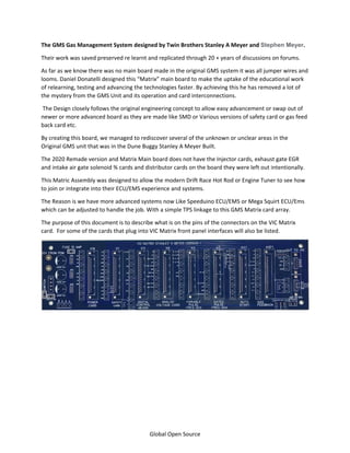
  • 1. Global Open Source The GMS Gas Management System designed by Twin Brothers Stanley A Meyer and Stephen Meyer. Their work was saved preserved re learnt and replicated through 20 + years of discussions on forums. As far as we know there was no main board made in the original GMS system it was all jumper wires and looms. Daniel Donatelli designed this “Matrix” main board to make the uptake of the educational work of relearning, testing and advancing the technologies faster. By achieving this he has removed a lot of the mystery from the GMS Unit and its operation and card interconnections. The Design closely follows the original engineering concept to allow easy advancement or swap out of newer or more advanced board as they are made like SMD or Various versions of safety card or gas feed back card etc. By creating this board, we managed to rediscover several of the unknown or unclear areas in the Original GMS unit that was in the Dune Buggy Stanley A Meyer Built. The 2020 Remade version and Matrix Main board does not have the Injector cards, exhaust gate EGR and intake air gate solenoid % cards and distributor cards on the board they were left out intentionally. This Matric Assembly was designed to allow the modern Drift Race Hot Rod or Engine Tuner to see how to join or integrate into their ECU/EMS experience and systems. The Reason is we have more advanced systems now Like Speeduino ECU/EMS or Mega Squirt ECU/Ems which can be adjusted to handle the job. With a simple TPS linkage to this GMS Matrix card array. The purpose of this document is to describe what is on the pins of the connectors on the VIC Matrix card. For some of the cards that plug into VIC Matrix front panel interfaces will also be listed.
  • 2. Global Open Source Index (Editing in Process) • Safety Jump Card Plugs into K1 Page 2 • K2 Connectors on VIC Matrix Card Page 5 • K3 Gated Pulse Frequency Generator Page 8 • K8 Connectors on VIC Matrix Card Page 11 • K11 Connectors on VIC Matrix Card Page 13 • K16 Connectors on VIC Matrix Card Page 16 • KGF1 Gas Feedback Control Page 19 • KA1 - Auto-Start Page 22 • Main Board Matrix Pin out Connectors Page 24 • Main Board Matrix Pin in Connectors Page 26 Here we Show the Basic Concept of how we separated the Gas on demand controls and the ECU /EMS portion which is now easier with modern Ems ECU systems. This allows a simple linking by the RPS signal and basic in/out sensor leads.
  • 3. Global Open Source The purpose of this document is to describe what is on the pins of the connectors on the VIC Matrix card. For some of the cards that plug into VIC Matrix front panel interfaces will also be listed. Note: The numbering on the 37 sub-d in table below start with pin 19 at top of VIC Matrix board K1 Connectors on VIC Matrix Card The K1 connectors on the VIC Matrix Card are for the Safety Cards. Card can be either the local Safety Jump Card or the Operational Safety Card which support other functions and remote control of the safety function. Pins in use on the 37 pin sub-d connector vary depending on the card inserted in the connector. K1 pins in 37 pin sub-d connector listed in table below are directly connected to board connections points on left of the K1 37 pin connector (see picture below) VIC Matrix K1 board section
  • 4. Global Open Source Pin # K1 Name Connectors to Left Description 19 12V GND Input from 12V Power Regulators 18 5V 5V Input from 5V Power Regulators 17 10V 10V Input from 10V Power Regulators 16 GND 12V Input from Power Regulator GND 15 NC 14 PRESSURE 13 NC 12 TEMP 11 NC 10 RPM 9 NC 8 JAR 7 NC 6 OIL 5 NC 4 12V GND Output on and off board devices when jumped by Safety Card 3 5V 5V Output on and off board devices when jumped by Safety Card 2 10V 10V Output on and off board devices when jumped by Safety Card 1 GND 12V Output on and off board devices when jumped by Safety Card 20-37 NC Note: Pins not listed are not connected (NC)
  • 5. Global Open Source Ki Safety Control Card Plugs into K1 The Safety Card has switches and sensor triggers which close the power connections on the VIC MATRIX STANLEY A MEYER backplane card. Such as over speed RPM trigger, over heat oil trigger, over heat trigger, roll over mercury switch, or a switch that connects to remote grenade ring pull kill switch. When this card is removed there is no system power to the rest of the boards plug in the VIC Matrix board. Alternatively can can be replaced with Safety Jump Card. The board provides jumpers between input and output pins of the 37 pin sub-d connector. The following pins are in use: Pin # Board Name Description 19 GND Input from Power Regulators 18 5V Input from Power Regulators 17 10V Input from Power Regulators 16 12V Input from Power Regulators NC 4 GND Output on and off board devices when jumped by Safety Card 3 5V Output on and off board devices when jumped by Safety Card 2 10V Output on and off board devices when jumped by Safety Card 1 12V Output on and off board devices when jumped by Safety Card 20-37 NC Note: Pins not listed have no connections (NC)
  • 6. Global Open Source Safety Card Sensors and Switch Examples Plugs into Ki Safety Control Card Safety Jump Card Plugs into K1 The Safety Jump Card closes the power connections on the VIC MATRIX STANLEY A MEYER backplane card. When this card is removed there is no system power to the rest of the boards plug in the VIC Matrix board. In operational use this board can be replace with a board that connects to remote kill switch The board provides jumpers between input and output pins of the 37 pin sub-d connector. The following pins are in use: Pin # Board Name Description 19 GND Input from Power Regulators 18 5V Input from Power Regulators 17 10V Input from Power Regulators 16 12V Input from Power Regulators NC 4 GND Output on and off board devices when jumped by Safety Card 3 5V Output on and off board devices when jumped by Safety Card 2 10V Output on and off board devices when jumped by Safety Card 1 12V Output on and off board devices when jumped by Safety Card 20-37 NC Note: Pins not listed have no connections (NC)
  • 7. Global Open Source Bare Card Front Card Back Finished Card with male pins in connector Note: Pin type in connector is a builder option though pin on VIC Matrix need to be opposite sex.
  • 8. Global Open Source K2 Connectors on VIC Matrix Card The K2 connector on the VIC Matrix Card is for the Variable Pulse Frequency Generator Card K2. On the VIC Matrix Card, the pins on the 37 pin sub-d connector are not labeled, however, the labels do appear on the K2 card for these pins (show here for reference). VIC Matrix K2 board section Pin # K2 Name Connectors to Left Description 19 GND GND Input from 12V Power Regulators 18 5V 5V Input from 5V Power Regulators 5 NC NC 4 C to k3 C to k3 Output Frequency generated on K2 card 3 B to K3 B to K3 Output Frequency generated on K2 card 2 Q to K10 Q to K10 Output Frequency generated on K2 card Also connects to K2 Q to K10 connector on far right of VIC Matrix Card 1 G to K11 G to K11 Output Frequency generated on K2 card 20-37 NC Note 1: Pins not listed have no connections (NC) The is not enough space to left of the K2 37 pin connector to handle all the interface signals going to the K2 front panel so the follow signals from K2 card go directly to front panel. For more details see description of K2. This table also provide information on labels for front panel K2 Name Description Aux X Input to switch10x less than 2x Aux 2X Input to switch 10x less than 3x Aux 3X Input to switch10x 10x less that 4x Aux 4X Input to switch10x Highest Freq Aux COM Output from switch to COM which routes to C Accel X Input to switch10x less than 2x
  • 9. Global Open Source Accel 2X Input to switch 10x less than 3x Accel 3X Input to switch10x 10x less that 4x Accel 4X Input to switch10x Highest Freq Accel COM Output from switch to COM which routes to B Resonant Run X Input to switch10x less than 2x Resonant Run 2X Input to switch 10x less than 3x Resonant Run 3X Input to switch10x 10x less that 4x Resonant Run 4X Input to switch10x Highest Freq Resonant Run COM Output from switch to COM which routes to Q Resonant Dist. X Input to switch10x less than 2x Resonant Dist. X Input to switch 10x less than 3x Resonant Dist. X Input to switch10x 10x less that 4x Resonant Dist. X Input to switch10x Highest Freq Resonant Dist. COM Output from switch to COM which routes to G GAS Switch to select Gas setting WFC Switch to select WFC setting for Freq. POTB NC POTA 100k pot Freq Adjustment side1 LED - Negative lead to LED LED + Positive Lead to LED POTB 100k pot Freq Adjustment Gas side of switch POTA 100k pot Freq Adjustment WFC side of switch GAS Switch position for GAS WFC Switch Position for WFC COM Connects GAS or WFC resistor bank to 555 Pin 7 Note 1: Wires on 100K Pot need to connected so frequency is changed in correct direction H-CW and L-CCW. Note 2: Need to verify Switch Name Com goes to correct board output name for all 4 switches. Need to do this so correct switch name is place on switches on front panel for each output. Note 3: This is case where name are not very helpful in telling you what they do. I expect these were original functional names and were never updated.
  • 10. Global Open Source K2 Variable Pulse Frequency Generator Card K2 Variable Pulse Frequency Generator Card – Populated without front panel interfaces
  • 11. Global Open Source K3 Gated Pulse Frequency Generator The K3 connector on the VIC Matrix Card is for the Variable Pulse Frequency Generator Card K3. On the VIC Matrix Card, the pins on the 37 pin sub-d connector are not labeled, however, the labels do appear on the K3 card for these pins (show here for reference). VIC Matrix K8 board section Pin # K3 Name Connectors to Left Description 19 - - 18 - - 17 A A Gated pulse out To K3 A on far right of board 16 - - 15 - - 14 - - 13 10V IN 10V 12 - - 11 - - 10 K To KGT K Left Connector 9 8 7 6 5 B/AUTO B/AUTO K2 Pin 17 (Manual Interface) 4 +5V +5V++++++ 3 GND GND 2 M/MANUAL M/MANUAL To M1 Connector to left of KGF1 From M Connector to M1 left of K8 From K11 Pin 19 (Auto Interface) 1 - - 20-37 NC Note: Connection not shown have No Connection NC Note: Connections with “-“ are directly connected signal ? Note: B/Manual and M/Auto labels are switched. Manual signal comes from K3 and Auto signal from K11. Problem can be fixed by wiring of front panel switch. Wiring on VIC Matrix is correct.
  • 12. Global Open Source K3 Off Board connections to front panel K3 Name Description LED Led + Led - ACCEL Input M1 from K11 MAN Input Manual in B from K33 SWITCH Selection returned to board SIGNAL Voltage level into chip to set gate frequency H/L Center Position of Pot 100K POT VDD into Pot CELL ON Switch Open (single pole switch) CELL OFF GND Switch closed SWITCH NC TEST Single A put from Gate Generator GHD Note: The 100K pot needs to hooked up so CW raises frequency and CCW lowers it NOTE: There are signals going on the 37 sub-d connector that go chips on the board as they are not labeled sure what they are. K3 Gated Pulse – Freq Gen bare board
  • 13. Global Open Source K8 Connectors on VIC Matrix Card The K8 connector on the VIC Matrix Card is for the Analog Voltage Generator Card K8. On the VIC Matrix Card, the pins on the 37 pin sub-d connector are not labeled, however, the labels do appear on the K2 card for these pins (show here for reference). VIC Matrix K8 board section Pin # K8 Name Connectors to Left Description 19 M M Gated Digital Signal in To test jack on front panel through Analog/Digital Switch 18 5V 5V 17 50K POT 50K POT Manual Speed Cal - Other side is GND on front panel 16 12V 12V On left as it goes to one side of 25K Pot 15 NC 14 RUN ACCE RUN ACCE On leg of switch 13 NC 12 GND GND 11 GND 10 GND 9 NC 8 NC 7 SWITCH SWITCH Manual Speed Cal leg of Switch 6 NC 5 100K POT 100K POT 4 J J Analog signal out in sync with gate To K8 J on left end of board and to DB9 pin 3 next to it not labeled To test jack on front panel through Analog/Digital Switch 3 NC 2 100K POT 100K POT Gain Limit – Other side is J on front panel 1 25K POT 25K POT RPM IDLING – Other side is GND on front panel
  • 14. Global Open Source 20-37 NC Note 1: Pins not listed have no connections (NC) Note 2: Pots on front panel need to be checked so there are wired to have the desired results increase CW decrease CCW Note 3: The front panel also has Analog/Digital switch the controls the M and J signals going to test jack on front panel. K8 Analog Voltage Generator – bare board
  • 15. Global Open Source K11 Connectors on VIC Matrix Card The K11 connector on the VIC Matrix Card is for the Digital Control Means Card K11. On the VIC Matrix Card, the pins on the 37 pin sub-d connector are not labeled, however, the labels do appear on the K11 card for these pins (show here for reference). VIC Matrix K11 board section Pin # K11 Name Connectors to Left Description 19 M1,M2 M1,M2 Pin 37 18 - - 17 (below M4) To Man/Cal 50K Pot on top of card 16 (below M2) 13 GND Pin 12 & 11 System GND 12 GND Pin 13 & 11 System GND 11 GND Pin 29 System GND 9 J Pin 9 J 37 M1,M2 Pin 19 36 M4 M4 35 M2 M2 34 M3 M3 33 J J 32 31 30 GND To System GND 29 28 5V 5V To System 5V 27 J TPS - TPS Connectors on right in of board 26 J TPS ~ TPS Connectors on right in of board 25 J TPS+ TPS Connectors on right in of board 24 J 23 22 12V 12V To System 12V 21 20 G G Input from G to K9 on Connect to Left of K2 (Timing signal in from K2)
  • 16. Global Open Source + ~ - Note 1: Pins not listed have no connections (NC) K11 Off Board connections to front panel Note: As the output of these show NC it appears these are not being used. These functions all are on K8 Analog Voltage Generator Card. K11 Name PIN Description ACCEL MAX 100K 1 J from P32 2 J from P32 J To Pin 1 A side of A to D Switch 3 Back into board IDLING 25K POT 1 Pin 7 GND 2 J 3 Pin 14 NC MAN/RUN SWITCH 1 From Pin 4 NC To MAN/CAL 50K POT pin 3 2 Pin 10 NC 3 To MAN/CAL 50K POT pin 2 MAN/CAL 50K POT 1 From Pin 4 NC Pin 3 NC 2 From MAN/RUN SWITCH pin 3 3 From MAN/RUN SWITCH pin 1 To BNC Pin 2 + DIGL/ANL 1 J from ACELL MAX 100K pin 2 2 BNC pin 1 3 IC1 pin8 BNC 1 - (GND) From DIGL/ANG switch pin 2 2 + Signal selected by DIGL/ANL switch From MAN/CAL 50K POT Pin 3
  • 17. Global Open Source K11 Digital Control Means - bare board New Daughter Board Replaces the k7 Laser Accelerator card to allow modern industry standard TPS sensor input to the GMS and K11 Circuit Assemblies. Designed to be simple use and to allow industry 3 pin plugs male and female TPS wiring loom plugs and join to the wiring loom of all cars easily.
  • 18. Global Open Source K16 Connectors on VIC Matrix Card The K16 connector on the VIC Matrix Card is for the Regulated Power Supply K16. On the VIC Matrix Card, the pins on the 37 pin sub-d connector are not labeled, however, the labels do appear on the K11 card for these pins (show here for reference). VIC Matrix K16 board section Pin # K11 Name Connectors to Left Description 19 - Shunt 1 on board 18 12V 12V 17 10V 10V 16 NC NC 15 5V 5V 14 NC NC 13 GND GND 12 NC 11 - Shunt on board 10 NC 9 12V 12V 8 NC 7 10V 10V 6 NC 5 5V 5V 4 NC 3 GND GND 2 NC 1 NC 20-37 NC Note: Pins not listed are not connected (NC) K16 Off Board connections to front panel K16 Name PIN Description ROTRAY SWITCH 1 To BNC + test point
  • 19. Global Open Source 2 Left 10V Blocking Diode 3 Left 5V Blocking Diode 4 Right 10V Blocking Diode 5 Right 5V Blocking Diode BNC TEST POINT 1 BNC - 2 BBC + 10V LED GREEN 1 - Top half 10V Status light 2 + ON/OFF SWITCH 1 Normally off – turned on if fuse fails 2 5V LED GREEN 1 - Top half 5V Status light 2 + 10V LED GREEN 1 - Bottom half 10V Status light 2 + FUSE 1 Fuse for bottom half 2 5V LED GREEN 1 - Bottom half 10V Status light 2 + Note: If power Regulators are off board then there would be 3 additional connections to each one.
  • 20. Global Open Source K16 Regulated Power Supply Bare Board
  • 21. Global Open Source KGF1 Gas Feedback Control The KGF1 connector on the VIC Matrix Card is for the Gas Feedback Control Card. On the VIC Matrix Card, the pins on the 37 pin sub-d connector are not labeled, however, the labels do appear on the Gas Feedback Control card for these pins (show here for reference). VIC Matrix KGF1 board section Pin # KGF1 Name Connectors to Left Description 19 VEE VEE 10V 18 M1 M1 Input Frequency from K2 17 GND GND System GND 16 10V INPUT 10V INPUT 15 11/12 OUTPUT 11/12 OUTPUT 14 K – GATE PULSE CARD K Out to K3 cell on/off control 13 NC 12 12V + 12V + VCC + 12V Input 11 12V - 12V - VCC – 12V Input (GND) 10 VEE VEE 10V To Trans Signal Input VEE lower right 9 SIGNAL SIGNAL Sensor To Trans Signal Input Signal lower right 8 GND GND System GND To Trans Signal Input GND lower right 7 OUT 6 OUT 6 Out to K3 input 6 6 NC 5 NC 4 NC 3 NC 2 NC To J on left side of K8
  • 22. Global Open Source 1 NC 20-37 NC Note: Pins not listed are not connected (NC) KGF1 Off Board connections This board was designed to support off board connections directly from the board these connection points are shown here. Most of these points are also in the 37 sub-d connector and on the connectors to left. KGF1 Name PIN Description VEE Cell pressure gage M1 Cell pressure gage GND Cell pressure gage 10V INPUT 11/12 OUTPUT K Limit Selector 1 2 3 12V + VCC 12V Input 12V- VCC 12V Input VEE Transducer Signal Input SIGNAL Transducer Signal Input GND Transducer Signal Input 6 VIC OUT 6 Note: Limit Selector is the only item that does not have an interface point on VIC Matrix board.
  • 23. Global Open Source KGF1 Gas Feedback Control bare board This is the Original Gas Feed back card from Schematic KGF2 Gas Feedback Control board was card found in the GMS not completed to db37 yet 90% done
  • 24. Global Open Source GF3 Gas Feedback Control bare board This is the Les Banki Alternate Gas Feed back card to show and allow choice using linear scale gas controls. Can control Throttle position.
  • 25. Global Open Source KA1 - Auto-Start The KA1 connector on the VIC Matrix Card is for the Auto-Start card. On the VIC Matrix Card, the pins on the 37 pin sub-d connector are not labeled, however, the labels do appear on the Gas Feedback Control card for these pins (show here for reference). VIC Matrix Auto Start board section Pin # KA1 Name Connectors to Left Description 19 NC NC 18 12V DC 12V 12V Input + 17 16 15 GND GND 12V Input - 14 13 12 11 10 Press Sensor Press Sensor 2 line pressure sensor input To AUTOSTART GAS SWITCH on lower right in of board 9 Press Sensor Press Sensor 2 line pressure sensor input To AUTOSTART GAS SWITCH on lower right in of board 8 7 6 NC 5 NC 4 RC ON/OFF RC ON/OFF Remote on/off To Out TO ECU 9 pin connector pin 8 3 RC ON/OFF RC ON/OFF Remote on/off To Out TO ECU 9 pin connector pin 7 2 NC 1 NC 20-37 NC Note: Pins not listed are not connected (NC)
  • 26. Global Open Source Auto Start bare board The Auto Start board will start cell and once cell or fuel rail reaches the correct pressure the engine starter will receive signal to start engine. Also incorporated into this Les Banki inspired Board is now a water auto refill and tank levelling circuit, example could be boats plane winds, or different shaped tanks or cell array pairs, can also be used to adjust the optimum capacitance levels of water. We can use water proof ultra sonic distance sensors as the water and cell and tanks are a high voltage environment preventing resistance sensors being use with out risk of shorting or ground electron back to cell or water/gas fuels.
  • 27. Global Open Source PIN OUT Connectors Connectors on right end of VIC Matrix Board The right end of the VIC Matrix has some additional connectors for off board interfaces. VIC Matrix bare board section for right in of board The TRANSDUCER SIGNAL INPUT is part of KFB1 section, and its pin out is shown in KFB1 section. The AUTOSTART GAS SWITCH is part of KA1 section, and its pin out is shown in KA1 section. TPS signals all come from K11 through TPS Block the four signals all go to the 9 sub-d connector next to it labeled OUT TO ECU and also has the labeled signals. 1 Db9 goes to the Vic Trigger card and through to VIC array of 10 VICs. Power rails are provided on db9. 2nd Db9 goes to the ECU/Ems Note the TPS also goes out to Hydruino ECU/EMS ( Speeduino) or the ECU /EMS controlling ignition and timing on engine which has not advanced a lot since Stanley A Meyer’s time. Pin # 1 Q from K2 2 J 3 J 4 J 5 NC 6 12V 7 AUTOSTART RC ON/OFF 8 AUTOSTART RC ON/OFF 9 GND
  • 28. Global Open Source NOTE: Are there 3 J signals in this connector? The 3 source pins are all tied together on the K11 card I have seen jumpers between small row of connectors on back of K11. I verified this with a ohm meter. I also verified that the TPS pins do go the 33,32,31 of the 39 pin connector The OUT TO VIC 9 sub-d has the labeled signals and is also directly connected to connectors next to it. Pin # 1 A from K3 2 VEE 3 J from K8 4 GND 5 6 12V 7 10V 8 5V 9 GND The WATER LEVEL has no connections
  • 29. Global Open Source PIN in Connectors Connectors on left end of VIC Matrix Board The left end of the VIC Matrix has the input power connectors. VIC Matrix bare board section for left in of board we have allowed for 3 full sets of power rails and jump points. NOTE: Large pads should be labeled. Noted they are +/- from the PDM safety pull ring This section has landing pads for the 2 switches and 2 fuses and large landing pads for the 12V FROM PDM input. The relay for 12V, 10V and 5V regulars to right of large capacitors feed the off board connects on bottom of board (right in picture above). The regulators for the rest of the board are on the K16 power card to right additional off board connectors are available from that card and are shown in the bottom of the picture above. See section on K16 for more details.
  • 30. Global Open Source Vic Transformer Array Trigger Boards The Vic Trigger Board will connect from the DB9 and split to 10 DB9 on the Vic Daughter Boards. It contains a TPS trigger sequence in Parallel for turning on and off the power rail to the 10 Vic transformers.
  • 31. Global Open Source GMS Matrix Main Board Circuit Cards In depth Review
  • 32. Global Open Source K2 Main Frequency Generator Board in depth review Description of the K2 Main Frequency Generator Board used in Stanley Meyer’s Water Fuel Cell Simple explanation of the function of this card it provides 4 separate frequency to other components. A base frequency and 3 others that are direct divisions of the basic frequency which is generated on the card using a 555 Timer. As configured the center frequency output from the timer is 1.2k with a 90+ % duty cycle and a period of about 830ms. Selection of which frequency to use is done manually using switches on front panel of this card. The output labels on circuit diagram below show up as inputs on other Stanley modules. The card is (PCB K2) or and labeled Module K2 in Stanley Meyer’s functional diagrams. Note: the test points on card to allow a scope probe to used (wire loops)
  • 33. Global Open Source The circuit for the card (Note: I used this drawing as it is cleaner than others one difference is the 10M ohm resister that was added on the version to clean up output signal from 555) Card Inputs: 1. There is only one electrical input to the card: 5 VDC. (Note: This is shown on Stanley’s drawings as VDD) 2. There are 5 manual inputs a. 100K Pot that controls the frequency output and duty cycle of the 555 Timer b. There are four switches that controls the frequency (1 of 4) to be sent to selected destination. i. Accel Control ii. Water Injector iii. Gated Pulse Freq Generator iv. K3 Card Outputs: There are 5 electrical outputs from the card. The fours frequency outputs can take on 4 states 1. Signal to turn on the LED on front panel (Red light Pulse Indicator) 2. Frequency selected by front panel switches (each switch setting is independent) a. G to K11 Accel Control b. Q to K10 Water Injector c. B to K3 Gated Pulse Freq Generator d. C to K3
  • 34. Global Open Source Circuit Functional Description Left to right. The resisters and capacitor control the output of 555 timer. The 555 timer is used to generate the base frequency as it wired to operate in the “astable” mode (see data sheet for explanation). The frequency output is control by the resisters and capacitor (.01u standard value) to the left of the 555 (normal labeled R1 and R2). In this case R2 is 1K and R1 is a pot that controls the range and period of output. As Using 4.7K resisters plus a 100k pot with allow a frequency range 1.295KHz to 12.658KHz with center at 2.350KHz. The calculator at the following link can be used to determine 555 output values for the different settings of the 100k pot. I left screen shots calculator here as it shows the Periods of the pulses as well. NOTE: First version of this document had R1 and R2 switched. I check for error when I was rereading Stanley’s WO 92/07861 which said out put should be over 10KHZ.
  • 36. Global Open Source https://circuitdigest.com/calculators/555-timer-astable-circuit-calculator The 10M resistor on the 555 output is used to clean up noise on the output signal (note this is not in the original circuit drawings). The voltage of the 555 is negative pulse at the level of the VCC input. The Three 7490 Decade Counters are used to divide its input by (10). This allows 4 separate frequencies to be available on the 4 selector switches. 1. 4X is output straight from the 555 Timer 10KHz 2. 3X divides 555 Timer output by 10 1KHz 3. 2X divides output of first 7490 by 10 50Hz 4. 1X divides output of second 7490 10 5Hz Note: The 7490 divisor is hard wired to divide by 10
  • 37. Global Open Source “It can be used as a divide by 10 counter by connecting QA with (clock) input2, grounding all the reset pins, and giving pulse at (clock) input1. This enables the cascade connection of the inbuilt counters.” This came from the data sheet when I first looked at data sheets, I missed the comment about cascade counters and did not understand that the output of the timer is a clock pulse and not a 50 percent duty cycle pulse. Note: I have now built and tested the circuit and can verify this is the it works. I have added screen shots below to show output of each of the 4 stages before and after the final inverter step. While the 555-timer output is a pulse the output of the 7490 is a 50% square wave. This means the frequency input to each 7490 is divided by 10. Note: Now the labels on switches make sense as the output of the last 7490 is the lowest frequency and output of 555 is the highest. The 7404 IC is used to invert the signal going to all 5 outputs so output pulse from card is positive pulse. The 270-ohm resister reduces voltage going to LED. Note: Circuit is wrong, when I hooked it as shown the LED was always on. Thought about it then decided it should go to ground and not to VCC. This worked and makes sense as the output of the inverter is a positive +5 V pulse. Led shows circuit is functioning. For Reference Screen shoots of the four stages.
  • 38. Global Open Source For all screen shots I have set the base frequency of the 555 Timer to 10KH with the control pot. Note: the voltage is high as the 5-volt regulator has not arrive yet. I did some testing and verified voltage level for the timer and the invert follows VCC input level. Output of 7490 does not Hooked up both channels of my oscilloscope to card so I can show the out right of the stage and also the output after in comes out of the invert which is what is output from the card. In all cases Channel 2 blue on bottom is initial signal out from device and Channel 1 Yellow on top is the inverted board output. Yellow pulse is always positive. Blue pulse is always negative. Reason for inverter as last step. This is 555 Timer Output (Position 4x on switch) Note: Frequency is 10Khz Output of First 7490 (Position 3X on switch) Note: Frequency is now 1KHz
  • 39. Global Open Source Project Output of Second 7490 (Position 2X on switch) Note: Frequency is now 102Hz Output of Third 7490 (Position 1X on switch) Note: Frequency is now 10.1Hz
  • 40. Global Open Source Project K3 Gated Pulse Frequency Generator Board in depth review Gated Pulse Frequency Generator Functional Description This document is a functional analysis of the Gated Pulse Frequency Generator. The purpose was to better understand its role in the Stanley Meyer’s water cell system and what function does it perform. Simple answers: 3. Switch on front panel turns on/off frequency signal going to cell by stopping output of IC SN7408N – Tested works 4. Switch on front panel select either: a. Manual mode - signal comes from Main Frequency Generator card or b. Accel - signal comes from Accelerator Module or another external source 5. Signal Pot sets width of frequency pulses in following range 3.102msec to 36.102msec. Note: this setting applies to both frequency sources. From Testing actual range a little different see pictures at end of document. 6. Provides an interface to let other modules turn off the cell Input (K) – Tested works 7. Creates the Gate wave train with its own frequency 8. It does NOT pass the input wave train. This is based on building and testing the board. 9. Signal out does not change much with input frequency. More test results and pictures of wave train at end of document. Picture and circuit are from Stanley Meyer’s estate above and circuit diagram below. Note the first 2 IC are in a 7402 IC.
  • 41. Global Open Source Project Document update 5/22/2019 Inputs to card: 3. 5 VDC to drive the electronic (VDD) on circuit diagram 4. 10 VDC (VEE) to provide power to Green LED on front panel 5. Switch on front panel to turn Cell On/OFF 6. Pot 100 K ohms on front panel to adjust pulse width labeled L H. It’s the 100 K ohms pot (Labeled VIC GATING ADJ on circuit) 7. Switch on front panel to select Man Input (B) or Accel Input (M1) from other cards 8. Input (K) from Gas Feedback Control Module (Allows external module to shut off cell) 9. Fuse on ground to protect IC A26 (SN 74122N) value unknown. Outputs from card: 1. Gated signal (A) to VIC module (Does NOT include input wave train signal) 2. Gated signal to light the Green LED on panel No light no gate. 3. Test point on panel to allow viewing output signal Functional Description of Circuit The resisters and IC on the card are used to bias the ICs and will not be discussed with the exception of the 100K Pot. Other items will be covered left to right as input signal enters on left and leave on right with exception of input K which comes in as a bias from the top in top of the diagram Input (B) is from the Main Frequency Generator Board and is one of the 4 frequencies that are generated on that card.
  • 42. Global Open Source Project Document update 5/22/2019 Input (M1) is from the Digital Control Means Module. For this analysis it is assumed input will be in the same range as can be provided from the Main Frequency Generator Board. The first two ICs on left are in a 7402 chip which contain 4 NOR logic gates only 2 are used. They are used in this circuit as and S-R Latch (Flip-Flop). See https://www.youtube.com/watch?v=mo4Lq0DvJ68 for good explanation of what they do as most data sheets do not explain why they are used. Simple explanation is they perform 2 functions 1) clean up the leading and training edges of the pulse to remove any noise in signal and 2) maintain the signal input at correct level for the SN74122N. NOTE as explained in the video NOR ICs can latch both the 0 and 1 states of the signal. Testing shows this only works correct when rest of circuit is functioning. Output locks up in low state if the pot sets the pulse width and frequency too low. There is a known lock up mode in a Flip-Flop used in this mode but when the rest of the circuit is working correctly this problem does not occur. I saw this problem in testing see test notes. IC SN74122N sets the size of pulse which is determined by the 100K Pot. This allows the size of the pulse width to be controlled from front panel 100K pot. From data sheet: Retriggerable Monostable Multivibrator Pin Function: An external timing capacitor may be connected between Cext and Rext/Cext. For accurate repeatable pulse widths connect an external resistor between Rext/Cext and Vcc leaving Rint open [unconnected]. To obtain variable pulse widths connect a variable resistance between Rint or Rext/Cext and Vcc. (This mode being used in circuit) The other resisters and capacitors around the chip set the bias conditions needed to support this function. Values shown in the circuit are selected to allow device to operate in this standard mode. The 1uF capacitor sets the formula that is required for this to be used do the calculation. I have included parts of the data sheet at end of this documents for reference. The equation we want is: Note: Be careful of units as equation expects input to have set exponents. Tw = 0.33 x Rt Cext Cext is 1uF or 1000000pF Rt = 4.7 + Pot + 4.7 So range is Low = 9.4 Center = 59.4 High =109.4 Tw low = 3,102,000ns or 3.102msec Tw center =19,802,000ns or 19.802msec Tw high = 36,102,000ns or 36.102msec
  • 43. Global Open Source Project Document update 5/22/2019 Cell off switch on front panel when in off position sets the state of the final AND IC in SN7408N to LOW. When the output signal is LOW there are no pulses generated. The (K) Input is assumed to act like another switch input to turn cell off based on external events. As I have not reviewed function of that module, I have not verified that this is in fact the case, but testing shows if (K) goes low it does turn off output. Other drawings of this circuit do not show the (K) input so it appears it was added to support additional functions. I believe it may be used to turn cell off when pressure gets too high. Q11 2N3904 amplifies the output signal and feeds it to the following: 1. The Test Point on front panel 2. Lights the Green LED which also gets 10 VDC from an external source. I found that using 5 VDC lights the LED which pulses with signal. Pulse rate changes as the frequencies of the gate wave changes when pot is rotated. 3. Gate Signal (A) to the VIC Note: There are chips on the card that do not appear to be used by this circuit. Do not know why, it is possible that they supported a function no longer needed and card has not been updated. Just like the (K) input looks like it was added later.
  • 44. Global Open Source Project Document update 5/22/2019 Details of SN72122N from data sheet
  • 45. Global Open Source Project Document update 5/22/2019
  • 46. Global Open Source Project Document update 5/22/2019
  • 47. Global Open Source Project Document update 5/22/2019 Results of initial testing: 5/21/2019 Test setup: 1. Variable Frequency Generator (K2) board I built from Stanley’s circuit. This is now a bread board version where all the contacts are soldered. It is complete except for Frequency selector switches (I ordered wrong ones). For the testing I used jumper cables to select the frequencies from each of the 4 stages. Board had been tested earlier to verify it is functioning correctly. 2. Gated Pulse Frequency Generator (K3) board also built from a Stanley’s circuit diagram. The was in bread board plug in type. 3. 5 VDC output switching power supply which provide power to both boards. I also checked system with a 9 VDC battery which was only putting out 7 volts and got same results. 4. Rigol DS1052 Digital Oscilloscope 2 channel 50MHz 5. Various connector cables and jumpers. Initial tests and Results 1. Rechecked the Variable Frequency Generator Board (K2) to be sure it was working. a. Set Pot on board to generate 5KHz signal out of the 555 Timer b. Hooked up output signal to be 500Hz c. Verified the frequencies of the all 4 stages were: 5Khz, 500Hz, 50Hz and 5Hz. d. Did note change I had made to LED to connect it to ground instead of +5-volt seems to introduce some noise on signal. I will do more testing on this issue later, but it was small enough that it did not affect tests. e. Tested jumper connections to make sure I could select each of the frequency on output. Verified with O-scope. 2. Connected K3 board with jumper cable and the plugged-in power using jumpers from K2. Board K3 powered up and Green LED turned on and started pulsing. Checked with scope that I had a pulse wave train but did not pay much attention to it yet. 3. Decided to check the cell off switch function first used a jumper cable to pull pin to ground as I had not yet hooked up a switch. This worked and signal out went to flat line as expected. 4. I next check the (K) input. As I did not have (K) source I hooked input up +5V through 10K resister as that is how other inputs to AND were configured, that worked as signal was getting through. To test to see it does turn off the cell (output of the circuit), I disconnect the resister and that worked as expected and signal out went to flat line. However, when I plugged it back in signal did not come back. 5. Trouble shooting why no signal turns of I bumped the POT and it was loose in the circuit as it is on a plug-in board and pin where just plugged in. Plugged back in and still no output. I thought I may have blown something when I unplugged it as I did not have a signal in more coming out of the Flip- Flop when I check it. I spent several hours trying to get the Flip-Flop final output to generate a pulse. I disconnected everything and tested path through all the gates on chip and they all worked. Hooked things up using different combinations of the NORs same results. Checked the capacitor and it was OK. Try hooking it up without capacitor did not work. Neither did swearing or yelling at it. Tried a different jumper cable to see if I had a bad plug-in connection and when I did that, I bumped the pot and green light blinked so I knew rest of
  • 48. Global Open Source Project Document update 5/22/2019 circuit was OK though. Input using this connect was this flaky. Then I turned POT all the way to lowest setting and green light was pulsing again. I returned everything back to original configuration as light stayed pulsing and continued testing. a. What I have figured out. The down stream SN74122N must be working and when it is it provides feed back to the Flip-Flop (output of second stage also input to first stage) which then cause it to create a pulse on the output pin. This solves the know lockup problem with the Flip-Flop. While this is documented I did not expect the feedback. b. Also remembered that I had set the POT to zero when I started testing. When I reset the lose pot on the bread board, I had centered it and it turns on this was the real cause of the problem. Further testing show that the POT has a very narrow range of operation. Zero on POT to less than a quarter turn (more on signal later). When you go beyond that signal flat lines and the light goes out. I had done all the trouble shooting with pot in the center. This explains why there is a green light on board if it goes out there is no gate being generated. 6. Tests on signal output. a. At zero setting of POT (POT reads 0 when tested with ohm meter) you get the highest frequency pulse and the longest period. As you increase POT resistance in the POT the frequency goes down. Highest value was around 40Hz and it went to around 5Hz then signal flat lined and LED went off. Only took about a quarter turn on POT for this to happen. As the signal went down the LED pulsed slower. b. The Output signal was not what I expected. I had expected a 50 % pulse and that the board would change the width of the pulse. This is not the case. In fact, it appears this to a totally different wave train and it looks like this board generates the gate for the system. Adjusting the pot adjusts the size of the gate. See O-scope screen shots pictures below. c. Then tested effect of changing input frequency. As I was using the K2 board as my input source, I tested each of the 4 frequencies to see what would happen. Results surprised me the output changed very little. I included screen shots of this as well. 7. LED shows pulses when there is a pulse train available and is off when there is none. Note: I used the 5 VDC supply not 10 Volts show on circuit diagram. I assumed that new LEDs do not need the higher voltage and LED did work. What I do not know is the 10 volts on signal is need downstream. As this is a change to original circuit, I wanted to note this. 8. Conclusions so far: a. Board appears of function as designed and does what its names implies. It generates the gate wave train and that is only thing it does. b. The board output does not appear to be affected much by frequency of input. c. Gate frequency and period are adjusted by the POT d. As the frequencies generated by K2 do not pass through K3 I am not sure yet how it gets to VIC. There is a Q to K10 out of K2 labeled Water Injector in that circuit diagram, but I have not seen Q input on any of the circuit drawings I have. I have not seen an original drawing for the VIC. e. I also notice that changing the POT on K2 is not a something you can do quickly because of the very small range and after each change you need to several seconds for signal to
  • 49. Global Open Source Project Document update 5/22/2019 settle. It’s change pot setting, wait, look at scope and change it again. Very difficult to get a desire value. f. Did one last test, tried 50K ohm pot in place of the 100K could not get it to pulse at all. 9. At this point, I am satisfied enough with the initial test that I will move parts to a hardwired board and continue testing. O-Scope Pictures: This is near lowest frequency before signal disappears and lowest frequency for K2 at 5Hz. Notice Period and Freq values are at bottom on picture. Note: Pulse width and Frequency changes slightly at all settings so some of the difference you see in pictures is due to that but there is about 4ms change between lowest and high frequency on K2 2 Same setting on Gate board 50Hz on K2 Same Setting of Gate Board 500Hz on K2
  • 50. Global Open Source Project Document update 5/22/2019 Same setting of Gate board 5KHz pulse on K2 Next set of pictures I have changed K2 to 500Hz and adjusted the POT on Gate board to show what changes Gate at 23Hz sorry for difference in screen size had to adjust scope to get signal on screen again. Watch how period changes with frequency as frequency goes up period goes down.
  • 51. Global Open Source Project Document update 5/22/2019 This is the lowest setting on the K2 POT and the lowest period I only did a couple of these as adjustment is very touchy and you must wait after doing each one, as it take several seconds for signal to stabilize after moving POT. Big change initially, as you can see capacitors in circuit change state.
  • 52. Global Open Source Project K8 Analog Voltage Generator Board in depth review Analysis of Analog Voltage Generator with WFC with Test Results Analog Voltage Generator Description Simple explanation of what it does. The best way to look at this circuit is to view it as having three separate functions. 10. An amplifier front end stage and receives a digital pulse wave signal and forms a reduce peak-to-peak signal, approximately 1-volt peat- to-peak (PTP) at a higher base voltage which is passes to last stage 11. The last stage receive input from first stage then sets an upper and lower limit on voltage levels of signal using input from Pots on front panel (Accelerator and Idle Pots). In doing this it also set the offsets needed by the 741 to keep the signal being clipped. 12. The third function is used for calibration and is switched in/out by switch on front panel. When in use Cal Pot can be used to set levels of pots in last stage or it can be used to set levels of settings down stream of this card. Its’ output is a flat line voltage which can be increased or decrease by Cal Pot. This picture below shows front panel and both the Digital Control Means Card and Voltage Generator Card (daughter board) and the circuit diagram for the Voltage Generator. Inputs 10. Pulse train (frequency set elsewhere) in this case starts in Variable Frequency Generator 11. 50K Pot for Manual Speed Cal 12. 100K Locking Pot that sets RPM Idling Level 13. 100K Locking Pot that sets Max Accel Level 14. VDD (+5 VDC) input to first 2 amplifiers Q1 and Q2 15. VCC (+12 VDC) input to second amplifier Q3 and A21 (741 Opamp) 16. Ground Note: The lower switch labeled Digital/Analog and the Test BDC Jack show up in the Digital Control Means circuit. The two cards share the front panel. Output 1. Output Signal J which goes to Analog Voltage Control Card
  • 53. Global Open Source Project Circuit Analysis The resisters through the circuit set the bias levels for the different amplifiers and are selected to provide a very specific result. The system is setup to operate on the trailing edge of the input pulse as indicated by the dot on the trailing edge of the input signal shown on the circuit diagram. Q1 and Q2 operate as a pair to form a balanced first stage amplifier (standard function for this arrangement) using the 5-volt and 12- volt supply to set the output level. They step up the input put signal and Q3 increase the amount of load the system can support. Q1 is a PNP transistor that amplifies the input signal – output is the wave train at 5 VDC at the voltage of the power supplied to Q1 Q2 is a NPN transistor that amplifies input signal from Q1 – output is the wave train at 12VDC at the voltage of power supplied to Q2. Note: To test this I supplied a lower level 10V to Q2 and that was the signal level of output. Q3 is a MPSA20 which is a NPN transistor is a second stage amplifier and has 12 voltage as it supply. The output of the Q3 along with resistors and capacitors is a signal with a 5-volt range 0-5VDC with a PTP range of approximately 1V offset from zero approximately 3V. (This is shown in screen shots in testing section below) The output is connected to a switch on the front panel that selects either: Manual Speed Cal: This allows operator to manually adjust the voltage level of the output signal. This pot provides 2 functions: 4. Allows operator to manual change flat line voltage level to rest of system 5. Provides a controlled input to the 741 Op Amp below so the minimum and maximum voltage levels can be set during the calibration of the system. Run Accelerator: Select input signal modified by first stage to be selected. A21 in circuit is a 741 Op Amp Wired as a Voltage Follower (see figure below). This means that the voltage out follows the voltage in and is normal provides isolation between states. However, with the resister network on both inputs it does more. (Note: good video showing effect of these resistors https://www.youtube.com/watch?v=MtccB9K09ck ). These networks provide a DC offset to both the high and low voltages. Ronnie Walker in one of his posts talked this and noted that both the pots have locking nuts on them to fix values once set. Low Setting: Provide a minimum voltage for the accelerator function (see Idling RPM). Note: The operating range of 741 is set 0 to 12 VDC (0 to VCC) then pot sets level above the level to keep signal being clipped and raise it to set idle speed.
  • 54. Global Open Source Project High Setting: Sets level below 12V to keep signal from being clipped and lowers that to protection against providing to much voltage to be sent to system. NOTE: There maybe another VCC supply connect to A21 that is not shown in circuit. I have noticed several cases the IC chip operating supply voltages are not shown in most of the circuit diagrams and chips will not work without them. For 741 note in data sheet said these are usually not show as they are always needed.
  • 55. Global Open Source Project Test procedure and test results Plan is to test card left to right as that is the way signal flows through the circuit. While the normal input M comes from the Digital Means Card, I do not have that card so instead I will be using the Variable Frequency Generator card that I built as my signal source. This will allow me to look at the signal levels seen at different frequencies. Test step Configuration: 5VDC (VDD in circuit) will be provided from a 9-volt battery driving a 7805 5-volt regulator 12VDC (VCC in circuit) will be provided from a 12-volt switching power supply as I had a couple from old computer equipment. RIGOL DS1052E – Duel Channel Digital Oscilloscope will be used to capture the wave train. Screen shots of signals at various locations through the circuit will included in test results. Scope’s computer interface will be used to capture screen shots as will the clip-it function in window to get information into this document. Variable Frequency Generator (Board K2) hard wired – Testing will be conducted using jumpers in place of the Switch to select frequency from the 4 stages. Done as I still waiting for correct switches. As the switch just select the frequency using jumpers should have not impact on test results. (Initial test were repeated with switches) Analog Voltage Generator will be a plug-in bread board version. NOTE: For this testing I will be using a 20K Pot to set the idle limit as I currently do not have a 25K POT if testing shows that level is too low of setting for this function I will add more resistance in necessary. It was and I added 5K to side of POT where it affected changes the least. There will be no connection to board output during this testing though I will look at signal at this point. Tests with Results: This first set of tests will be with K2 set up to use 50Hz output from card. Timer output on card was set to 5KHz so stages are: Stage 1 – 5KHz Stage 2 – 500 Hz Stage 3 – 50 Hz Stage 4 – 5 Hz Verify input from Variable Frequency Generator (K2). Jumper on K2 is set to output of state 3 which is 50Hz Channel 1 Yellow – Input to board Channel 2 Blue – Input to board Math Vmax (2) Blue – Max voltage level of Channel 2
  • 56. Global Open Source Project Check input to Q1 on base after 1K resistor Channel 1 Yellow – Input to board Channel 2 Blue – Input to Q1 Base Note: Signal PTP level reduce but top near 5 V Check output of Q1 Channel 1 Yellow – Input to board Channel 2 Blue – Input to Q2 Base Note: Signal Inverted
  • 57. Global Open Source Project Check Input to Base of Q2 after 1K resistor Channel 1 Yellow – Input to board Channel 2 Blue – Input to Q2 Base Check output of Q2 before 1 K resistor input to base of Q3 Channel 1 Yellow – Input to board Channel 2 Blue – Input to Q3 Base Vpp(2) Blue - Shows peak to peak voltage of channel 2 Note: Signal inverted again
  • 58. Global Open Source Project Check output of Q2 before 1 K resistor input to base of Q3 Channel 1 Yellow – Input to board Channel 2 Blue – Input to Q3 Base Vpp(2) Blue - Shows peak to peak voltage of channel 2 Check output of Q3 Channel 1 Yellow – Input to board Channel 2 Blue – Output of Q3 Vpp(2) Blue - Shows peak to peak voltage of channel 2
  • 59. Global Open Source Project Check output of Q3 after 47K resistor at input to switch (This is operational flow to rest of circuit) Note: Test done with switch set to manual mode so loading of rest of circuit not on output. Channel 1 Yellow – Input to board Channel 2 Blue – Output of Q3 Vpp(2) Blue - Shows peak to peak voltage of channel 2 Probe is between the 47K resister out Q3 and before 100k and cap from ground. Voltage step on scope was adjusted to 500mV just to see change in signal. Check output from card Scale was set back to 5 volts Note: Peak to peak level is 1 volt and level is above 10 volts so signal is getting through
  • 60. Global Open Source Project Check the effective Max Accel and Idle Pots (Goal was to set limits on pots before checking output of card. (This shows using operational signals to set limits on clipping will show Cal signal later) The screen shot below shows idle pot to have a base voltage around 4 volts. This can be change from above 10 volts to low about 2 volts. Not sure of operational range should be. The 2-volt level is a close as you can get to zero as that is the lower rail is a 0-volts and with 741 you can only get to within approximately 2V of the rail. If you get closer signal starts to get clipped. Notice Vpp(2) is around 1.2V
  • 61. Global Open Source Project Show signal being clipped at low setting of idle value Here is signal above where clipping starts shown at 1-volt division And signal is getting clip as you go lower Notice Vpp(2) values
  • 62. Global Open Source Project Signal Flat lines if you go to0 low Check effect of Accel Pot This one was little harder to show. Needed to set idle setting very high and change volts per division again to keep it on screen. If you go to high it starts clipping signal. I also moved channel 1 so we could see channel 2 better.
  • 63. Global Open Source Project This shows signal moved down by accel Pot This shows you can move it higher with idle pot, but signal is now getting clipped
  • 64. Global Open Source Project Calibration Path There is a direct line from the 12VDC input to Q3 but it also supplies 12 Volts DC to the100K Manual Speed Cal Pot. This is the reason these is no pulse on this line. Blue line in this case shows voltage of 12VDC source Blue line now shows voltage after the 100k resistor before the pot with pot set to counterclockwise setting L on switch I have added 2 cursors to help show what is happing the Yellow curser shows approximate location of 12-volt input source. The white cursor show the low setting of Pot In first screen shot below low setting the blue line is at the white line in second screen shot the blue line is slightly less than 5-volts above line. Blue line now shows output of pot set with switch turn max clockwise H on front panel.
  • 65. Global Open Source Project The last set of screen shots show that this pot provides an approximately 0 to 5 VDC source that can be used to input as a controlled DC level that can be used to calibrate down stream settings. It can be switched in and out as needed by switch on front panel. Note: The 5-volt DC output range of the Pot is consistent this the range of the output from Q3 that is input to the same switch. I did find using a voltmeter on output when using calibration setting was easier for me as I could see the values changing easier. When I did this, I had not yet seen the output wave train as I testing to see if I had the pots wired correctly (values increase clockwise and decrease counterclockwise). Given that there was a five-volt range I was trying set upper and lower limit close to 5 and 0. It did not work, if I set lower limit down close to zero it pulled down upper limit and it I set upper limit close to 5-volts lower limit had to be up. I also noticed that when I did upper limit close to 5 that there was only a little over 1- volt range between them. Made me wonder if I had resister values wrong. It was only after I worked on the actual signal that this made sense. The screen shot blow shows the operational output signal in blue and the input to board in yellow. I added the cursor lines to show CurA white line is 80 mV and CurB yellow is 3.92 V. So, you can see the output signal would be in that range I was seeing in the calibrate testing. After playing with using the Calibration Pot to set High and Low values I found that changing one effects the other and you must use idle pot to raise the level high before accel pot has an effect also Cal Pot also
  • 66. Global Open Source Project influences both. So, like a lot of other things it is a balancing act. Easier to see using a live signal with pulses as you can also see clipping. I took one more screen shot see below after I use live screen to set lower level and upper level so neither was clipped. I then switched to calibration mode and took screen shot below and saw lower limit and it was just above 2 volts which I expected (see blue line). One final series of screen shoots to show what output signal looks like when you change the input frequency. As I am using the Variable Frequency Board (K2) as a source of the signal, I do not have way to change the voltage level of the input signal. Scope will be reset to show frequency changes but only in horizonal scale. Note: I did do one quick test by doubling and halving 1K resister in front of Q1 neither seem to have an effect on Q1 output. Input set to 5 HZ (stage 4 and 1x on switch) Input changed to 50 HZ (stage 3 and 2x on switch)
  • 67. Global Open Source Project Input changed to 500 Hz (stage 2 and 3x on switch) Input changed to 5KHz pulse out timer (stage 1 and 4x on switch) Note: Output signal is at 12 volts. I expect circuit is not designed to handle this high of frequency and would not normally be selected as an analog input, but I wanted to show output for all four switch selections on Variable Frequency Generator board.
  • 68. Global Open Source Project Update from Hardwired version of circuit. Changed the way I went from plug jumper version to hard wired version in same format. First two boards I build I made the hardware jumpers as I built the circuits so when I went to hard wired version all I did was transfer jumpers and solder them in. This time I did not do that and had several errors I had to correct include one missing ground to one of the pots that took me a couple of days to find and things did not work right without it. After hard wired version was built, I took another set of screen shots of the output and got a little different results. Test at 50 Hz Yellow trace channel 1 – connected to input 5V/Division Blue trace channel 2 – connected to output 2V/Division Notice at 50 Hz we close to a sine wave at very low voltage but with a offset that can be move by idle pot. Test at 5 Hz Yellow trace channel 1 – connected to input 5V/Division
  • 69. Global Open Source Project Blue trace channel 2 – connected to output 2V/Division Scope adjusted to keep more of wave on screen Test at 500 Hz Yellow trace channel 1 – connected to input 5V/Division Blue trace channel 2 – connected to output 500mV/Division Scope adjusted again Test at 5K not done as output was already extremely low at 500Hz Not total sure why the slight drop in level in hardwired version but I found that to be very low as well. Being to thing it may be by design of the resistor and capacitor on the output of Q3. As it checked and the rest of the circuit handles a higher voltage pulse with no problem. Testing Information Notes: Most of the early screen shots where taken with the scope set to sync on leading edge. Later shots with it set to sync on trailing edge as I noticed dot on trailing edge on circuit diagram and I wanted to show
  • 70. Global Open Source Project the final results with it synced on trailing edge. As the signals stayed in phase through out this is not a factor in analysis of this circuit as a standalone board. I did find that Q1 and Q2 do not work correctly unless the downstream components are in place and Q2 output did not work until I hooked up the 12 supply. I did it this way as I was doing initial testing and I did not yet have all the parts was missing Q3 and the A21 and I was also double-checking wiring as I went through circuit. Also did not want to damage parts if I had it hooked up wrong already did that on one of the other boards. Test summary and Conclusions General conclusion is board I built and tested works and performs functions implied by labels on circuit diagram and from panel controls. It also matches with the general description of the function of this board in Stanley Meyers documentation WO 92/07861. It also matches with simple description at start of this document. Though to honest I updated that to reflect testing. Modified to change assumptions based on analysis to reflect actual results of testing mainly defined better the functions of bias resistors and capacitors. As whole purpose of the document and the testing was to determine what it does to input wave train, testing was a big success. It also verified functions of Calibration tool and operational limit settings work; 4. Modifies as standard 0-5 VDC PTP input pulse train and creates an approximately 1VDC PTP wave train of the same frequency and period with approximately 3VDC offset. This was the most important finding of this testing as the what the output of the circuit looked like was unknown. 5. Provides a means in last stage of circuit to change level of offset and to set limit on upper range. Testing verified this does work. This is an operational control to be able to provide limits for a specific use without changing downstream baseline settings. 6. Provides a means of calibration limits of last stage. More useful when you have some idea of what those limits need to be, but it does work. 7. One thing limited tested also showed is that it is unlikely that voltage level is used to do acceleration function as the Q1 output is set to 5 bolt pulse. 8. Finally, the screen shots show the effect of each element in the circuit as well at the finally output. Update to Results from hardwired version. Circuit still operates the same but the was a drop in the PTP voltage of the output. See added screen shots of output for the hard-wired version. I am beginning to expect that this may be by design and done on purpose. Stan appears to be very careful in select bias values and I wondered why the extra cap and resister on Q3 output that are connected to ground. The output still has the same offset and 2 volts plus. I also added 1K resistor across output and there was no change is signal.
  • 71. Global Open Source Project Note at 50 Hz the signal looks like a sign wave. At 5 Hz it a saw tooth wave and at 500 Hz it almost disappears as wave PTP gets smaller with increase in frequency. I find that interesting as this is called the Analog Voltage Generator Circuit and output is close to a sine wave. One caution: The circuit was tested with no output load. It is possible based on testing of this circuit that finally output levels may look different with a load as this happen with other elements in this circuit. This will be retested, and results updated when I build the Voltage Control circuit. That project has already been started. ( I did add 1K resistor across output after finish board shown below and it did not affect output signal. Pictures of circuit as built Couple pictures of finished circuit after I moved components from plug in bread board version to hardwired version of same circuits. I am using these boards as it keeps the same lay out and they are cheap 3 for around $14. Also, means I did not have to deal with PC card design and fabrication. Power jumpers to make it easier to hook up power and less like to hook it up backward. Yep done that even when I was trying to be careful. Same reason for blocks for signals on ends of board as I am not building back plan for card connections. One construction note: Solid core wire for connections to POTS and switches was a bad idea. Removed them and used strained wire. As shown mission round to top side of pot on left.
  • 72. Global Open Source Project VIC Transformer Card & Daughter Board In Depth
  • 73. Global Open Source Project Sections of Main Vic Card Analysis and Test Results of Phase Lock Circuit K21 The main purpose of the Phase Lock Circuit is to find the resonant frequency of the cell and lock on it. The method it uses allows the system to adapted to changing conditions in the cell, temperature, containments in water, different water sources etc., which all change the exact resonant frequency. The Phase lock circuit has a lot of things happening in it. This circuit has more interfaces than any of the other circuits and those interfaces directly affect its functions. If you look at the VIC controller card it contains not only K21 but almost of the circuits, it interfaces with as well. I chose to build those circuits as separate cards, so it was easier to understand and test them. In this case, I could not do that as K21 will not function properly without some of the inputs from other cards. While I had not planned it that way I had built and tested all those except the Pulse indicator circuit K14. As I had the circuit cards I used them to support testing of K21 with the exception of K14 as it requires a coil for its input which I do not have yet. You can look at K21 as having 4 separate pieces 13. The input and output section the receive signal (A) the gate pulse and gated pulse. This is a series of NOR gates. First conditions the gated pulse (A) the second combines it with (G) and they make up the inhibit signal to the CD40046B with creates the gate in the output when the both signals are high. 14. The CD4046B which is the heart of the circuit. It has three main parts see discussion below. It interfaces with all the inputs and outputs which it generates. 15. The Lock section is a series of NOR gates that condition the Lock signal before sending it to K22 and drives the LOCK LED. 16. The series of 3 frequency dividers each step the frequency down by 10 and also drives the OSC ON LED. The 4-position selector switch on front panel is also part of the group. While the has been some speculation that this is part of the Phase Lock Loop (PLL) function I am not sure it is as my testing show the PLL functions works with using the dividers and they are not configured they way they would be in part of the PLL. My guess it they may be used to condition the cell by providing different frequency. In the input and output sections I cover all the interface including those required to run the chips. In the analysis in testing section I will cover all the inputs and outputs and have include screen shots showing what the all look like as this was one my basic goals of building the circuits. To completely understand this process, you also need to be aware of what is happening on the other boards that generate input signals. In this document, I will limit the depth of the analysis of those circuits as I will cover them in more details when I analyze those boards. I have not included an in-depth analysis of the CD4046B as it is a very complex chip, however, I have included a few references I used that were a great help to me. I do discuss it a very high level so I can talk about the interfaces it used. Note: In building and testing the circuit I found that several values, mostly capacitors, are missing others in the forum had found that information and published in this forum. I have included reference to it below. It was a huge help as I could not get CD4046B to work without the values.
  • 74. Global Open Source Project Note: I also found that I had a lot of trouble getting the PLL function to work. It turns out this function uses phase information of the signal to find resonant lock. This CD4046B turns this information into voltage levels and uses voltage levels to create the frequencies. The bias resistors and capacitors are used to determine the operating and scanning ranges. Reason I mention it here is the putting the LED’s on the same voltage sources causes problems in getting PLL to work reliably. I moved both LEDs to a separate 10-volts regulator and I was able to get the system to lock. In some of the other circuits, the LED are shown on 10 volts source which was the reason I tried it here. Inputs 17. Gated Pulse Frequency (A) from K3 18. Gated Signal (G) from K21 (output fed back into CD4046B on pin 3) 19. Resonant Feedback Signal (H) from K14 20. Frequency Adjust control on Front Panel 21. Voltage level (F) from Resonant Scanning K22 a. Not locked – Double ramped voltage pulse b. Locked – Voltage level need to generate signal at resonance from input (E) 22. VCC +12VDC (From -12VDC switching power supply in my case) 23. Ground 0 VDC 24. +10 VDC for LEDs – Shown as 12 volts on circuit diagram but that cause noise problems as it puts spike is source voltage Outputs 6. Gated Signal (G) to Cell Driver K4 7. Voltage Level (E) CD4046B is voltage VCO is using to create the current output frequency. This voltage level sent to Resonant Scanning K22. 8. Lock Signal (L) to Resonant Scanning K22 Low - no lock High - Locked 9. Signal to Front Panel Lock IN Red LED 10. Signal to Front Panel OSC ON Green LED
  • 75. Global Open Source Project Circuit with values from estate information Circuit Analysis Almost everything feeds into or comes out of A27, a CD4046B chip. I found this application reference to be very useful in describing what the chip does. It gives a couple of uses for the chip besides the normal data sheet spec information. http://www.ti.com/lit/an/scha002a/scha002a.pdf . There is a lot going on in this chip and the description in the beginning of the reference document does a very good job of describing what it does, and I not going to try and repeat here. However, I will highlight a few things and try to point out what type of signal to expect on each of the inputs and outputs as that is what I will be looking at in my testing. First a general comment about why this chip. It performs Phase-locked loops (PPLs) testing to keep signal a specific frequency within some selectable range and uses low power as stated in this quote from Section 1 of reference “The PLL described in this application report is the CD4046B, which consumes only 600 μW of power at 10 kHz, a reduction in power consumption of 160 times when compared to the 100 mW required by similar monolithic bipolar PLLs.” This contributes to the low input power needed to drive the cell which appears to be one of Stan’s prime goals. The block diagram below from the same reference show the direction of the signals on each of the pins. Note: There is an error in diagram Pin 4 is out not in.
  • 76. Global Open Source Project Pins in CD4046 and use in Phase Lock Circuit 1. Phase Pulses Out Scanner K22 Lock signal (L) 2. Phase Comparator 1 Out Scanner K22 Lock signal (L) Comparator In In This Frequency is output from pin 4, range selected by switch 3. VCO Input In Frequency from pin 4 or dividers (x10 each stage) 4. VCO Generated Freq Out Combined Gate Pulse (A) and (G) signals 5. Inhibit In Normally Low – High with (A) and (G) are both low 6. Voltage from C1 Input to setting center range of VCO 7. Voltage form C1 Input to setting center range of VCO 8. VSS In Ground 9. VCO In In Input (F) from Scanner K22 (Required for VCO to work) 10. Not used 11. VCO Resistor to GND Out From 50K POT to set center frequency and scan range 12. VCO Resistor to GND Out Resistor to GND another input for operating range 13. Phase Comparator 2 Out Across Resistors to (E) then Cap to GND (this is a voltage level) 14. Signal In In Current Operation Frequency (H) in from K14
  • 77. Global Open Source Project 15. Not used 16. VDD In +12 VDD (can be +5 to 15 VDC) The 4001 on top accepts signal (A) gate pulse frequency generated in the Gated Pulse Frequency Generator (K3) using the operational frequency used in the Digital Control Means circuit (K11) or K3. The first stage NOR gate conditions the (A) signal and passes it to the second stage with merges it with the (G) signal, carrier frequency, generated in this circuit. The combined signal is passed to the CD4046B pin 5 (inhibit). The result is normally low which allows the VCO to generate a frequency. When low both (G) and (A) are low VCO output is stopped and gate created in signal. As the (G) signal changes it is fed back into the 4001 and process repeats keeping the carrier frequency in sync with the gate pulses. The 4001 on bottom of the circuit receives phase information from the output of the 2 Phase Comparators in the CD4046B and combines them. When signals are in phase a lock signal is passed by the NOR to the second NOR. The diode and resistor between the two NORs pulls the signal down so only a solid Lock signal gets through to the second NOR. The second NOR drives the Lock LED and sends the Lock Signal (L) to Resonant Scanning K22 to switch its output. The 50K pot on pin 11 and the .1uf capacitor on pins 6 and 7 set the center frequency of the Voltage Controlled Oscillator (VCO). This center frequencies is sent out pin 4 to the three 4017 chips which each divide its input by 10. They do the same functions as the chips in Variable Frequency Generator (K2). The output of the 4 stages goes to the front panel switch. The switch selects which of the frequency ranges is provide as the output signal (G) and fed back in pin 3 of the CD4046B as the current operation frequency. The output signal also drives the Green LED on front panel to indicated that the system is on. The big difference from K2 circuit is there the frequencies are set directly from the POT on front panel. Here the POT sets the initial center frequency, same process, but here the operational frequency is scanning to fine resonance. Scanning voltage control pulse (F) is used by VCO to generate frequency, exception is if Manual Mode is selected on K22 then POT on K22’s front panel is used to select frequency to be output by VCO. The comparators in the CD4046B compare the current signal against prior state and then generates a new voltage that tells the VCO which way to adjust the output voltage. The VCO make the change and the cycle repeats. In there is no input signal the VCO defaults back to the preset center frequency. There is a fair-sized true table that is followed during this process. For more detail see the referenced document which does a good job of explaining how it works. Note: The import thing here is the phase of the input signal (H) not the signal level as is it searches for pulse edges. Test Plan At this point I have all the circuits built but the Digital Means circuit which I currently do not plan on building. However, I have not yet tested the Pulse Indicator circuit, so I do not have the input from that device to support testing of this circuit. As the input to the CD4046B is the frequency of the signal on the core I plan on using a second CD4046B to manually generate a frequency to be used to test the Phase Lock Loop (PLL) functions. PLL with try to lock to this frequency. What I do not have testing this way is a input (H) that is also varying while (G) is changing.
  • 78. Global Open Source Project I will be testing the circuit first with no other inputs but power. Goal with be verify the function of the control POT and the frequency generation and dividers. I believe this should work standalone, (it didn’t work as VCO need input on pin 9) I should also have a (G) signal I can look take an initial look at. Then I will add the (A) gate signal from K3 which means I will also need K2 hooked up to drive it. This should give me a look at the final form of the (G) signal as it will have but carrier and gate information. I will be using another CD4064B in VCO mode to simulate frequency of the resonant back signal (H) if that works, I should be able to verify the (F) and (L) signals. A reminder, my primary goal is to see what signals look like as the move through the circuit and to see how the signals are changed based on the input device receives. Test step Configuration: Bread board version of the Phase Lock Circuit K21. 12VDC (VCC in circuit) will be provided from a 12-volt switching power supply as I had a couple from old computer equipment. Testing showed I also need 10VDC used LM317 to provide it directly to LEDs RIGOL DS1052E – Duel Channel Digital Oscilloscope will be used to capture the wave train. Screen shots of signals at various locations through the circuit will included in test results. Scope’s computer interface will be used to capture screen shots as will the clip-it function in window to get information into this document. Variable Frequency Generator (Board K2) hard wired and tested version. Will generated frequency needed to drive (K3). May use the output of a separate switch to select frequency to use for resonant testing as I do not have a signal generator. I will note this test where it occurs. Alternate will be to use a second 4046 in VCO only mode as I built a standalone circuit to verify 4046 was working. I have several chips so can use this circuit to generate another frequency to do lock testing. One of he referenced videos was doing this. Turns out second V046 was easier to use for this test as I wanted a 4KHz signal and needed K2 at lower frequency to drive K3. Gated Pulse Frequency Generator (Board K3) hardwired and tested version. Will generate the gate pulse signal (A). Bread board version of the Phase Lock Circuit K21. Resonant Scanning Circuit (K22) Build and tested. Will use it in testing to verify interfaces on both boards. Will verify interfaces (F), (L), and (E). The (F) voltage signal will be extensively used in verifying PLL functions. Note: Also found that PLL works better when (F) can contain the (E) signal. So it also needed to be hooked up and working. Tests with Results: Test setup changes to add signal (A) The initial tests of the A signal will be with K2 set up to use 50Hz output from card. Timer output on card was set to 5KHz so stages are: Stage 1 – 5KHz
  • 79. Global Open Source Project Stage 2 – 500 Hz Stage 3 – 50 Hz Stage 4 – 5 Hz Verify input from Variable Frequency Generator (K2). Switch on K2 is set to output of state 3 which is 50Hz Channel 2 Blue – Output from board Verify that K3 is output pulse (A). in the desire range. Check that LED is pulsing and use scope to set frequency in the desire range. Capture (A) before Zener Diode CH2 – blue input to board (A) CH1 – yellow input before Zener diode Capture (A) after Zener Diode, Inputs 12 and 13 of first stage of 4001
  • 80. Global Open Source Project Capture output 11 of 4001 Ran into a problem was not able to get pulse through the 4001. If you look at the scope traces you can see the reason. Pulse is offset from zeros so 4001 never sees the zero state. I did try one of the frequencies directly from the K2 board and that worked so I knew 4001 was OK. There was a note by the Zener diode that it was added because of the LED on K3 which also added a pull up resistor. Next question was what size Zener? Researched articles on Zener diodes, ones that talked about using Zener diodes to reduce voltage had the answer. I had purchased a box of Zener diodes as it was only a few dollars more than buying a few, the smallest one was 3V which is what I used as I did not want to reduce voltage too far. That solved this issue, but I was not getting any output from the next stage of the 4001. But I had only the one input as I was not getting the (G) signal out of circuit. NOTE: The desired output of the second stage is the low state. That is because the signal goes to the inhibit pin 5 of the CD4046B. The low state allows the VCO function to operate and high state stops its output. The only time that happen is when both inputs to the 4001 NOR are low. Turns out the problem was not that signal voltage was too low issue was it was not high enough to trip the gate, so it did not let the pulse through. Signal of first stage never goes high so no pulse. It’s a NOR so output is always High (more detail below in testing section). So, I switched trouble shooting to why no output on pin 4 of the CD4006B. Decided to take it out of the circuit and test it standalone so I could use known inputs. Along the way I found a couple of good videos about using the 4046. This one does is very good and easy to understand overview with scope shots showing what the 4046 is doing to lock on resonance. https://www.youtube.com/watch?v=SS7z8WsXPMk One of thing I like is it talked about each of the three functions of the 4046 it pointed me to look at the VCO is the initial step in my search for why no signal. One of the other videos even showed using a second 4046 as another signal source to test the phasing. I will do this in my testing as this circuit to test lock functions and outputs. While this video shows impact of changing components to the VCO operation it did not really show you the configuration being used to make it work. As I was just trying to get a signal on pin 4 I wanted to know how to do that. I kept either getting nothing or a 12-volt flat line signal. More research found several items on just using the VCO to generate a signal. This one helped a lot https://hackaday.com/2015/08/07/logic-noise-4046-voltage-controlled-oscillator-part-one/ But I wound up using the circuit from this one though there is an error in diagram pin 4 and pin 11 functions are reversed. https://www.eleccircuit.com/the-100-hz-to-10-khz-square-wave-generator-by-phase-lock-loop-ic/ Reason I liked this one is it showed I had another issue I needed to address, and it also provides clear guidance on choosing values for bias resistor and capacitors. Turns out you need the (H) input for the VCO to function, which I did not have hooked up. NOTE: Also helps if you hook up VDD and VSS correctly. I had reversed them and took a long time to find this as I drew breadboard circuit wrong. Built it according to my drawing wasn’t until I compare it to test 4046 that I caught it. Cause by pin 8 be labeled VSS instead of ground.
  • 81. Global Open Source Project The circuit also showed an easy method to provide voltage by using a POT which is what I did to test the chip and experiment with values for the resistors and capacitors. In doing all this I found I either had gotten a bad chip or had damaged it not sure which (like damaged as I has ground and +12V backwards). But I had purchase 2 so I am continuing testing with the good one. I am finding getting the center range set is a real pain. Either I get real low ranges below 1Khz or I can easily get real high ranges 20-50KHz but trying to get ones about 4-12Khz is proving to be difficult. Main issue is the capacitor values as it is real sensitive to this value. It has been stated in other threads that the CD4046B has a narrow sweep range and I am seeing that. Also, adjustments are very touchy a slight change in VIC Gating Adjust POT makes a big change. After quitting for the night, I got thinking given that circuit has the divide by 10 chips following it so the output of the second stage would be 5KHz, so as signal seems to be more stable in the range that may be where we want to set the center range. So today I add the POT back to input 11 and replaced the resisters I was using for testing with the ones from K21 as I wanted to see what the range is with those values. Answer is it depends on level of the voltage on pin 9. By setting both at max value I can get 250KHz at min voltage I get 30 KHz. If I set the voltage so I get 100Kz without changing the resistance POT, then I can go as low as 32.5Khz using resistance POT. It was easy to then set it at 50KHz and it gives a fairly stable frequency and dial is not as touchy. I spent a lot of time changing resistor and capacitor to try getting into correct range. Even trying using 50KHZ as center planning on using stage 2 of signal dividers. Problem with this was there is a big mismatch in timing with control scanning voltage (F) form K22 and 50KHZ signal. There was about a 4 second gap between scans so system was not likely to ever lock on resonance. One advantage of using Stan’s circuits and values is it showed 50KHZ was wrong frequency. But also, big problem in this circuit as values for several of the capacitors are not shown on diagram. Fortunately, others in the forum have solved that issue and found missing values see document at this link. Using correct values solved a couple of different issues and I was able to get system to lock using my test setup. Will cover that below. Re: Understanding SM Driver Circuit, Building A Test Driver Voltage control Board 9.Reply #143, on December 20th, 2016, 09:24 AM »Last edited on December 20th, 2016, 09:31 AM Quote from haxar on December 19th, 2016, 12:39 AM New revised manual adjusting VIC schematic: http://open-source-energy.org/?msg=41523 I have not done any testing on the circuit that generates the (H) so I am not sure what normal voltage level for that signal is yet. I expect 12+ volts as that is the output level of VCO. Output has stayed steady at the level through all the testing even at zero volts. I just took at quick look at the Pulser Indicator Circuit K14, to see what voltage level out would be and I am still not sure as it comes out of the 918m, I know a 741 would be no higher that 10-volts but have now worked with this chip yet though I do have one coming from eBay. I do have the bread board of that circuit built just missing the 918m but do not know yet how I am going to test it without a core and coil.
  • 82. Global Open Source Project This may be more detail than people are looking for, but it is things I wanted to know as it tells we why these values and what happens when you make a change to the controls. NOTE: Turns out H is frequency signal and voltage level does not matter as long as it is high enough to do a phase check. I used both a 12v and a 10v signal and it did not change PLL test at all. Testing of Output of CD4046B Pin 4 This is to test the function of the CD4017 dividers to see it they are function properly. For this phase of testing I have disconnected most of the outputs from the CD4046B and I am using an external voltage source to provide voltage on pin 9 so I get a signal out of the VCO. I have set the center frequency using the resistance to 50KHz. Capture the output of 4046 pin 11 before entering first 4017, switch setting 4 CH1 Yellow 5V/Div connected to output of 4046 pin 4 A27 CH2 Below 5V/Div – Input to 4017 A28 pin 14 (probe at output of switch) No change in signal as expected but verifies wiring all the way through switch I could not get any to the 4017 to work thought I had done something to them. Setup to test them standalone. Found a quick and easy circuit that would allow me check if bad or not. I had a few extras so was going to start testing with them. When I got package out, I read label to see it was correct one. It was the one I was looking for, but I found I had ordered wrong ones they were 40174s a different chip. Ordered correct one will be here in a few days $6 for 15 on Amazon. I might be able to do some other testing with of the 4046 as they way I built the circuits I had to use two breadboards as I put all the 4017s on a separate board for space reasons. I think I can check the resonant functions without them. At least the lockup part as I now have Resonant Scanning board tested so I can use that.
  • 83. Global Open Source Project Reporting mistakes as well as what worked. Keep trying to figure out why I could not get 4046 to work in circuit. I put in test circuit I built, and it worked. Put it back in circuit and I could not get pin 9 to work. Finally, after several hours found I had hooked up ground and +12v backwards. Surprising this did not damage chip. Diagram I was using to layout breadboard had pin 8 labeled Vss instead of GND. As both pin 8 and pin 16 were colored red I missed this. In my mind if 8 was power then 16 had to be ground. Funny thing is I wonder why this chip was different than others. Lucky these chips are cheap. I am using a 1nF capacitor to get a center range of 50Khz. I set this using Manual mode of K22 and Freq Adjust POT on front panel of K21. As long as I had K22 hooked up I switched to Auto mode to see the sweeping action. The double ramp pulse out of K22 is turned into a sweeping pulse that varies from 33.8KHz to 78.5KHz on about an 8 sec cycle with 6 seconds of that being a pause. It ramps up very slight pause at top then ramps back down then pauses. If you look at input to pin 9 without changing scope all you see is the voltage going up and down, you do not see the double ramped pulse unless you slow the scope way down. Capture pulse at bottom during pause Done at the output of Switch on front panel. Switch set to 4x the output right out of pin4 of CD4046B Capture pulse near top of sweep Blurry screen is due to slow update rate to computer display of scope
  • 84. Global Open Source Project Capture Pin 9 double ramped pulse I slowed the scope way down to show input (F) on pin 6 from K22 that is creating the scan this is the double ramped voltage pulse. Show here slowed down to show what is driving the scan. Note: The lock LED comes on during the 4 sec pause then goes off when scan starts. I did check and the Lock signal is being sent to board but does not have much an effect on pulse as it is in sync with pulse. NOTE: I have left this 50KHz testing in here as it shows large range of CD4046B and also to shows 50KHZ to be wrong signal and why. I have already done some quick checks with new capacitor values from reference above and system is working much better. I will repeat VCO tests with new values below. Tried to Resume Testing after Changing Capacitor and Resistor Values those in Reference above At this point I have hooked up my Resonant Scanning Card K22, so I have (L), (E) and (F) all connected. I also have a CD4046B operating in VCO only mode. This gives me a frequency source I can used for the (H) signal. This will be the signal I will be using to test PLL function. At least that was my plan and worked to a point. All the interfaces worked, and I will show that below but while I could get the system to lock it was very touch and would not stay long and took a long time to resync when it dropped out. I spent a couple hours resetting ranges of sweep and voltages using the
  • 85. Global Open Source Project POTS on the front panel of both K21 and K22. That helped some but it would still not stay and lock and strangely it lock seem to change when I move in my chair. Finally found cause!! Power source for LED makes a huge difference on ability to CD4046B to lock on signal. After I got ready to test, I could not get system to stay locked in lock. Both external frequency source and VOC output were jumping around about 100Hz. I was using same 12 VDC switching power supply as source. After checking that everything was hooked up, I decided to power external 4046 with 10-volts from LM317 I was using on K22. With this change the frequency out of external 4046, which I was using for (H), became much more stable. But VCO pin 4 output was still moving around. I could get it into lock by touching my desktop, but it would not stay long and if I move it would drop out and take a while to resync. Finally, I notice one of the test leads I had on lock signal was touching the desktop. Moving it helped at little, also making the Lock connect more secure helped but did not solve the issue. As both helped, I thought about this connection some more. Per circuit diagram I had hooked both LEDs up to 12-volt source but had seen it in other places hooked up to VEE so I decided to try hooking it up to the 10-volt output of the LM317. As soon as I did this the system locked up and now stays in lock even when I change the frequency of external source. I can now make huge changes in frequency and they are tracked instantly. Here why I think this makes a difference the VCO is a voltage-controlled device. The LED switching on and off makes enough difference in the voltage source on the control POT to slight shift the voltage which causes the frequency out of the VCO to also move. The LM317 isolates the LED from this change and makes the system a lot more stable. Back to Screen Shots As I am setup to look at PLL function I will continue here Capture Output of VCO Pin 4 CH1 Yellow – (H) from external CD4046B (using 10-volt supply so output at 10VDC) 10v/Div CH2 Blue – VCO pin 4 output frequency Math function Purple - (A-B) CH1-CH2 Peaks show when out of phase
  • 86. Global Open Source Project Capture frequencies at high setting Turned up frequency – I did change frequency range with Freq Adjust pot as I had set it tighter when I was having problems Same scope settings only change was to pot setting to change range and to adjust Pot on external 4046 to change frequency Note the purple spikes are constantly changing as there are slight changes in frequencies Change frequency to low setting This is the lowest I could go but had to change the Control POT on front panel to lowest setting. But this also pulls down the high range so not a useful setting Capture 5KHz again after setting top range about 8KHz There is a limit on the range available it gets large as you increase Freg Adjust POT on front panel, but it also pulls up bottom range. System will not lock if you get outside range. 8-9KHz
  • 87. Global Open Source Project seems to give you a middle about 5KHz. You see this by setting Freg Adjust POT then changing 6. goes out of lock when you hit limits of range. You can also do this using Manual Mode and Manual Freg Adjust POT on K22. Capture E while in lock CH 2 Blue – 10v/Div Note: E is the voltage level required to generate a signal at locked frequency in the case 5.102kHz. Capture F while Locked CH2 Blue – Voltage level Looks a lot like E because it is E in locked mode
  • 88. Global Open Source Project Capturing F in unlocked mode would require completely changing scope settings but I will copy trace here from earlier testing for reference as you need to have scope set at very slow setting Capture L while in lock CH2 Blue – Voltage level High We are in locked state when signal is High
  • 89. Global Open Source Project Capture L while not locked CH2 Blue – Voltage level Low We are in unlocked state when signal is Low Received CD4017 today so added them to circuit after above testing. I am not sure what they do besides add voltage and noise to off delay and affect pulse width slightly. The next set of scope shot will show what I mean. Capture G stage 4x on switch CH1 Yellow – H input pin 14 CH2 Blue - G output of pin 4 Math Purple (CH1-CH2) to show phase What’s hard to show is the noise on top Yellow and Blue pulses and moving spikes on purple. Also, the pulse width are moving slightly can see this if you look at pulse in readings. I woke up the next morning thing about this and I think I know may know where the small spike on top of
  • 90. Global Open Source Project signal are coming from. I think it is the chips counting. They can be used to directly drive an LED with a pull up resistor which means they need to draw the current to do that putting a load on the voltage source. I only noticed this as I did earlier testing without them in the circuit and did not have these small spikes. Capture G stage 3x on switch CH1 Yellow – H input pin 14 CH2 Blue - G output of pin 4 Math Purple (CH1-CH2) to show phase With Scope set to trigger on Channel 1 With Scope set to trigger on Channel 2 As I expected this changes output frequency and we will be out of lock as my source did not change frequency which would not be the case in real system
  • 91. Global Open Source Project Set output frequency to 1Khz and change input frequency to 1KHz By adjusting frequency on source and center with Freq Adjust I got it lock but it has a very narrow search range. Capture 2x on scope CH2 Blue shows frequency stepped down by 10 I can not set my input any lower so this G2 at this setting normally H would follow.
  • 92. Global Open Source Project Capture 1x setting on switch CH2 Blue- G Output without gate Just to see what would happen I routed G/3 to input H pin 14 and got this I though it should lock up and it did. Will need to do more testing of this switch with the input from feedback circuit.
  • 93. Global Open Source Project Set system back to 5KHz to test impact of signal (A) input At this point I have finished test all the interfaces but (H), (A) and (G). I am mostly satisfied that the (H) interface is working but will do more testing much later when I have a valid input source for it. As everything else appears to be working though system does do a resync every 8 seconds. This is screen when in lock CH1 Yellow – My (H) input CH2 Blue – (G) on its output (no gate input) Math Purple – Shows the phasing difference between (H) and (G) and the spikes up and down are the voltage adjustments to keep signals locked. The addition negative voltage is because I am using 10 volts on 4046 providing the (H) signal. This shows a very solid lock. Before I removed the LED the spikes where large and both pulses and constantly moving.
  • 94. Global Open Source Project This is screen when searching CH1 Yellow – My (H) input CH2 Blue – (G) on its output (no gate input present) Math Purple- Here you can see the phasing difference Not sure if the scan every 8 second is a problem or not. I have seen a couple of references that this can be problem for some PLL devices if the edges are aligned to sharply. I need to do more research on this. It may be that my source signal is too stable not sure, but I wanted to report what I am seeing. Back to when I was trying to test input (A) so I could see affect on (G). Turns out I could not get it to work. Signal (A) is there but I could not get it through the first stage of 4001. I know the 4001 works as I used signal from 4046 test source to test it and it lets pulse through. When I got thinking about device and looking what I was seeing I realized signal not being zero was not the problem as output of 4001 was high. This is normal when inputs are both low and, in this case, both inputs are (A). This meant the sign was never going high enough to cause the 4001 to go low so no pulse. This caused me to look at the level of the input signal. When wired per diagram with 2.2k resister to ground Vmin 200mV, Vmax 2.8V and Vpp 2.6V before Zener and Vmin 0V, Vmax 800mV and Vpp 800mV after. I tried moving resistor to +12 to try and pull signal up instead of down and got Vmin 1v, Vmax 4V and Vpp 3.2V before Zener and Vmin 1.6V, Vmax 4.8V and Vpp 3V. From these numbers you can see wiring it the way that is shown on the diagram the Zener did what I thought it was supposed to do drop signal level to zero. But that leaves a signal that will never get through the 4001 even with the resister configured as a pullup, the level is just not high enough. I did get signal through using 10 ohm and even a 39 ohm pull up but not a good thing. They got extremely hot and in a little while fried value paint markings. Also, I am not happy with load they are putting on circuit voltage source. By the way voltage need to trigger was near 7V. Did not try to find exact range as I did not want to damage something else already did enough of that during this testing. So, I need different way to fix the interface mismatch. The mismatch really puzzles me as K21 is the only place (A) is used. I know this can be solved as this is done in Analog Voltage Generator Circuit K8.